
Resolving the stacking fault structure of silver nanoplates†
Taixing
Tan
 ab,
Shun
Zhang
a,
Jie
Wang
a,
Yuqin
Zheng
a,
Haopeng
Lai
a,
Jialiang
Liu
a,
Fengqi
Qin
a and
Cheng
Wang
*a
ab,
Shun
Zhang
a,
Jie
Wang
a,
Yuqin
Zheng
a,
Haopeng
Lai
a,
Jialiang
Liu
a,
Fengqi
Qin
a and
Cheng
Wang
*a
aInstitute for New Energy Materials and Low-Carbon Technologies, School of Materials Science and Engineering, Tianjin Key Laboratory of Advanced Functional Porous Materials, Tianjin University of Technology, Tianjin 300384, P. R. China. E-mail: cwang@tjut.edu.cn
bGanjiang Innovation Academy, Chinese Academy of Science, Jiangxi 341000, P. R. China
First published on 7th December 2020
Abstract
The stacking fault structure (SFT) is the key to understanding the symmetry breaking of fcc nanocrystals and the origin of two-dimensional (2D) anisotropic growth of nanoplates. After resolving the SFT in Ag nanoplates under aberration-corrected transmission electron microscope (TEM) observations, it is found that there are three basic stacking faults, namely, twinned stacking fault (SF-t), a layer missed stacking fault (SF-m) and a layer inserted stacking fault (SF-i). The SFT is composed of one or a combination of two or all of the three kinds of stacking faults with a total number varying from 4 to 9. It has been demonstrated that the SFT could generate concave faces, step faces and (100) faces in the lateral directions, which provides sites for adding-atoms with a higher coordination number than on the top and bottom flat (111) faces, and results in the anisotropic growth along the 2D direction. Additionally, Ag nanoplates fall into either center symmetry or mirror symmetry when the corresponding number is even or odd. The center symmetry and mirror symmetry with different side face arrangements in turn manipulate the shape evolution to cubes and bipyramids, respectively. Our study provides a comprehensive understanding of the formation and growth of 2D metal nanomaterials.
Introduction
Noble metal nanoplates or nanoprisms, a kind of typical two-dimensional (2D) metal nanomaterial, have received extensive research interest due to their unique properties and potential for application in tumor therapy,1–3 surface enhanced Raman scattering (SERS),4–6 sensing,7–10 bio-imaging,11–13 catalysis,14–16 and electronics.17,18 Targeting those applications, a variety of synthetic strategies, including thermal-/photochemical reduction synthesis,19–25 the polyol method,26 the template process27 and nanolithography,28,29 have been developed to synthesize 2D metal nanomaterials including Au, Ag and Pd nanoplates. Among them, chemical reduction synthesis is one of the most popular bottom-up methods with high throughput.24,30,31 Having a highly symmetric face-centered cubic (fcc) crystal structure, the formation and growth of anisotropic 2D noble metal nanomaterials are not thermodynamically favored.32,33 The origination of the 2D anisotropy of metal nanomaterials is perplexing. Pileni et al. firstly noticed the presence of forbidden 1/3{422} reflections in 2D Ag nanoplates, which originate from the stacking faults or planar defects, and suggested that the stacking faults might dictate their 2D anisotropic growth.34 This proposed growth mechanism has been gradually and widely accepted.Recently, it has been realized that the twin structure as one kind of stacking fault structure plays a pivotal role in the anisotropic growth of nanoplates.29,32,33,35 The presence of a single twin in Ag nanomaterials could lead to the formation of hexagonal nanoplates with convex and concave side faces alternatively at the early growth stage. The concave faces having a reentrant groove structure provide sites for adding atoms with a higher coordination number than on convex faces and flat faces, resulting in a faster growth along the lateral direction. The gradual shrinkage of concave faces because of their faster growth rate than convex faces leads to the formation of triangular nanoplates. On the other hand, when an even number of twins are present, both concave and convex faces could be formed at each of the six sides of hexagonal nanoplates. This allows equal lateral growth along all six directions.35 As a result, those nanoplates will maintain a hexagonal shape. The structure with convex and concave side faces of nanoplates partly explained the formation of the hexagonal and triangular shapes. However, no explanation and observation were provided for further anisotropic growth of the triangular nanoplates, once concave faces on the triangular nanoplates were depleted. As twinned stacking faults (SF-t), one kind of planar defect (stacking faults), usually coexist with other kinds of stacking faults including stacking faults with missed layers (SF-m) or inserted layers (SF-i),34,36 the contribution of these two kinds of stacking faults to the anisotropic growth is yet to be unravelled.
Some efforts have been made to characterize the stacking fault structure of nanoplates. For Ag and gold nanoplates, a lattice with a spacing of 2.5 Å could be observed frequently in powder X-ray diffraction (XRD) patterns, high resolution TEM images and electron diffraction patterns.34,36,37 The 2.5 Å lattice fringe is attributed to the 1/3{422} facet, which is theoretically forbidden in the fcc phase. The observed 1/3{422} facet in the fcc crystal was used to explain the presence of stacking faults.34 To directly investigate these defects in HRTEM images, the 2D Ag nanoplates need to “stand” on the carbon film. This allows one of the edges to be parallel to and the {110} planes to be perpendicular to the electron beam.36,37 With this orientation, the {![[1 with combining macron]](https://www.rsc.org/images/entities/char_0031_0304.gif) 11} facets show discontinuities as a result of repeated stacking faults between the {111} facets, which is direct evidence of the stacking faults.36 However, because of the limited resolution of the HRTEM facility, it failed to directly observe these planar stacking faults on the atomic scale and distinguish the atomic arrangements of the ABCABC… sequence. Very recently, planar stacking defects in Pd and Au nanoplates were directly observed with atomic resolution. For a single “standing” Pd nanoplate, a layer of three atom thickness stacked in a different direction from the main nanoplate was observed clearly by HRTEM analysis.26 Neretina and co-workers reported that multiple parallel twin defects were observed directly in gold nanoplates, but other stacking faults were hardly discernible.38 So far, those two reported stacking fault structures are individual cases and they differ from each other, which suggests that there might exist different kinds of stacking faults apart from twin defects and the structure could be complex. The lack of systematic investigation of the stacking fault structure on the atomic level makes it difficult to analyse the exact structure of planar defects as a whole and evaluate their effects on the anisotropic growth. Hence, it is urgent to resolve the stacking fault structure on the atomic scale to fully understand the origin of the anisotropy and shape evolution in growth.
11} facets show discontinuities as a result of repeated stacking faults between the {111} facets, which is direct evidence of the stacking faults.36 However, because of the limited resolution of the HRTEM facility, it failed to directly observe these planar stacking faults on the atomic scale and distinguish the atomic arrangements of the ABCABC… sequence. Very recently, planar stacking defects in Pd and Au nanoplates were directly observed with atomic resolution. For a single “standing” Pd nanoplate, a layer of three atom thickness stacked in a different direction from the main nanoplate was observed clearly by HRTEM analysis.26 Neretina and co-workers reported that multiple parallel twin defects were observed directly in gold nanoplates, but other stacking faults were hardly discernible.38 So far, those two reported stacking fault structures are individual cases and they differ from each other, which suggests that there might exist different kinds of stacking faults apart from twin defects and the structure could be complex. The lack of systematic investigation of the stacking fault structure on the atomic level makes it difficult to analyse the exact structure of planar defects as a whole and evaluate their effects on the anisotropic growth. Hence, it is urgent to resolve the stacking fault structure on the atomic scale to fully understand the origin of the anisotropy and shape evolution in growth.
In this work, Ag nanoplates were used for structure analysis and the stacking fault structure on the atomic scale was investigated systematically by utilizing aberration-corrected TEM. After examining nine nanoplates, it is found that there are three basic stacking faults including SF-t, SF-m and SF-i. A stacking fault structure could be constructed by one kind of these stacking faults or a combination of two or three of them with a total number varying from 4 to 9. Additionally, we have observed that if more than two SF-m or SF-i are connected continuously, a 2H or 4H hexagonal close packed (hcp) structure could be formed. It is demonstrated that the presence of the stacking fault structure would lead to the formation of concave faces, step faces and alternative arrangement of (111) faces and (100) faces at the surface of lateral sides. This kind of surface structure provides multiple growth sites for adding atoms with a higher atom coordination number than top and bottom (111) faces, and results in anisotropic growth along the lateral direction and a 2D plate-like shape. All those three basic stacking faults have made contributions to the anisotropic growth. Furthermore, it is also found that nanoplates exhibit two different symmetries along the 〈111〉 direction determined by the number of SF-t and could be divided into nanoplates with center or mirror symmetries. We have demonstrated that the symmetries determine the side face arrangements and the shape evolution of nanoplates in the vertical growth. Specifically, the mirror symmetry with an odd number of SF-t controls nanoplate growth into bipyramids, while the center symmetry with an even number of SF-t manipulates nanoplate evolution into cubes.
Results and discussion
Stacking fault structure of Ag nanoplates
A stacking fault structure (or planar defect structure) with multiple stacking faults in Ag nanoplates is stacked along the 〈111〉 direction and parallel to the flat (111) faces.36 Silver nanoplates with two large flat faces tend to lay flat on the carbon film during sample preparation. In order to directly observe the planar defect structure, the electron beam should align parallel to the lateral side and be oriented in the 〈110〉 direction, which requires nanoplates “standing” on the carbon film. For easily standing on the carbon film and electron penetrating through the nanoplates along the lateral direction, Ag nanoplates with an edge length of few tens of nanometers and a relatively low aspect ratio are ideal for TEM analysis.The silver nanoplates were prepared through a modified method developed by the Yin group.19,39 Ag nanoplates with high purity were obtained by fast reduction of AgNO3 with NaBH4 in the presence of H2O2, in which H2O2 served as the etchant to eliminate isotropic particles (details in the ESI†). As shown in Fig. 1a and Fig. S1,† plate-like particles dominate and most of the nanoplates are rounded triangles with an average edge length of 25 nm and a thickness of ∼7 nm. There are indeed some nanoplates “standing” on the carbon film, marked by circles. By tilting the sample, the orientation of the electron beam could be aligned along the 〈110〉 direction. As shown in Fig. 1b, three sets of lattice fringes with 2.36 Å, 2.36 Å and 2.0 Å intersected with each other, which were attributed to {111} faces, {11} faces and {010} faces, respectively. Additionally, a lattice fringe with a spacing of 2.45 Å corresponds to the well-known forbidden 1/3{2![[4 with combining macron]](https://www.rsc.org/images/entities/char_0034_0304.gif) 2} facet spacing (theoretical value 2.48 Å). The 1/3{22} facet was perpendicular to the (111) faces (Fig. S2†), which was usually observed with electrons aligning in the 〈111〉 direction. The {11} faces intersect with the (111) face with an angle of nearly 70.5° (Fig. S2†), which is consistent with the theoretical value. The planar stacking faults arising from the wrong stacking of the {111} faces lead to the disruption or change of the trace of {11} faces, which is marked by parallel black lines in Fig. 1b. Such discontinuity extends from the bottom to the top of the Ag nanoplate. Four additional “standing” nanoplates were investigated. From the high-resolution HAADF images shown in Fig. 1c, d and Fig. S3,† multiple stacking faults can be observed clearly for each of them. Although how the stacking fault structure in the silver nanoplate is formed is still unclear, the stacking faults are found almost in every single investigated nanoplate. As metallic silver has the lowest stacking fault energy among coinage metals,40,41 it is highly likely that the stacking fault structure is formed spontaneously at the nucleation stage in solution.
2} facet spacing (theoretical value 2.48 Å). The 1/3{22} facet was perpendicular to the (111) faces (Fig. S2†), which was usually observed with electrons aligning in the 〈111〉 direction. The {11} faces intersect with the (111) face with an angle of nearly 70.5° (Fig. S2†), which is consistent with the theoretical value. The planar stacking faults arising from the wrong stacking of the {111} faces lead to the disruption or change of the trace of {11} faces, which is marked by parallel black lines in Fig. 1b. Such discontinuity extends from the bottom to the top of the Ag nanoplate. Four additional “standing” nanoplates were investigated. From the high-resolution HAADF images shown in Fig. 1c, d and Fig. S3,† multiple stacking faults can be observed clearly for each of them. Although how the stacking fault structure in the silver nanoplate is formed is still unclear, the stacking faults are found almost in every single investigated nanoplate. As metallic silver has the lowest stacking fault energy among coinage metals,40,41 it is highly likely that the stacking fault structure is formed spontaneously at the nucleation stage in solution.
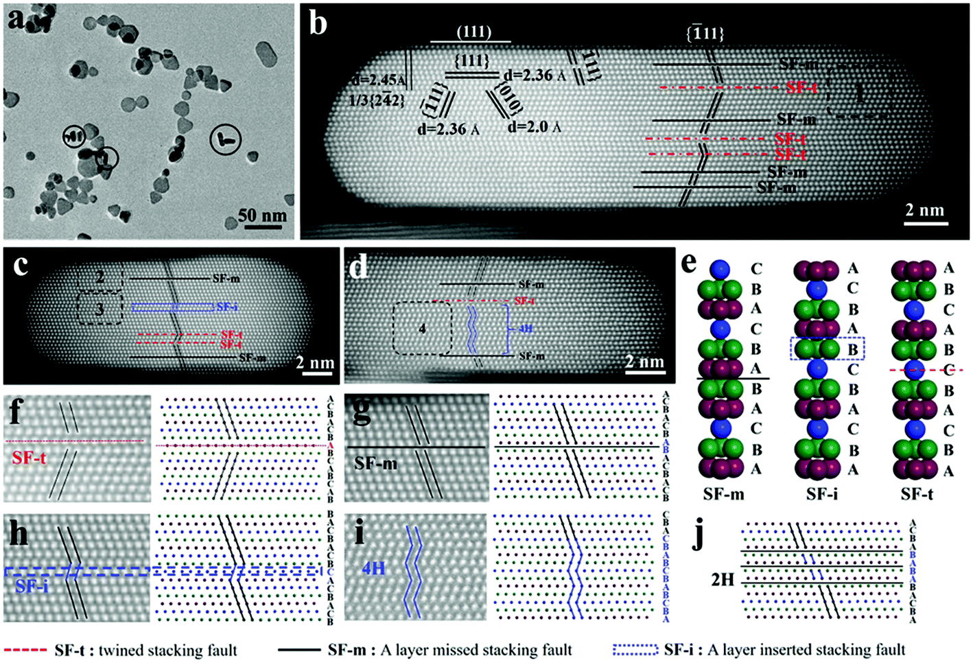 | ||
| Fig. 1 TEM analysis of rounded triangular nanoplates and crystal simulations. (a) TEM image of silver nanoplates. (b), (c) and (d) High-resolution HAADF images of “standing” nanoplates viewed from the 〈110〉 direction. (e) Simulation of three basic stacking faults: a layer inserted, a layer missed and twinned stacking faults. (f) Twinned stacking faults (SF-t) with the corresponding simulation. (g) A layer missed stacking fault. (h) A layer inserted stacking fault. (i) 4H phase and the corresponding simulation. (j) Simulation of the 2H phase. The uncontinuous parallel black line indicates the traces of {11} planes. | ||
In a perfect fcc Ag crystal, the atom layer is arranged strictly in the …ABCABCABC… sequence along the 〈111〉 direction. Any disturbance or changes in the ordered …ABCABCABC… would lead to the formation of stacking faults. In the …ABCABCABC… sequence, a layer was missed (or knocked out) from the …ABCABCABC… sequence, and a sequence of …ABC![[B with combining low line]](https://www.rsc.org/images/entities/i_char_0042_0332.gif)
![[C with combining low line]](https://www.rsc.org/images/entities/i_char_0043_0332.gif) ABC… or …ABC
ABC… or …ABC![[A with combining low line]](https://www.rsc.org/images/entities/i_char_0041_0332.gif) ABC… or …ABCABC… could be formed. The structures of those three situations are actually equivalent to each other because the names of A, B and C layers were defined by their relative positions. Therefore, a layer missed stacking fault (SF-m) could be expressed as a …ABCABC… sequence as shown in Fig. 1e. Similarly, a layer inserted in the …ABCABC… sequence would generate a …ABCABC… sequence (Fig. 1e), which is represented as a layer inserted stacking fault (SF-i). Additionally, a twin plane could be formed such as …ABCAB
ABC… or …ABCABC… could be formed. The structures of those three situations are actually equivalent to each other because the names of A, B and C layers were defined by their relative positions. Therefore, a layer missed stacking fault (SF-m) could be expressed as a …ABCABC… sequence as shown in Fig. 1e. Similarly, a layer inserted in the …ABCABC… sequence would generate a …ABCABC… sequence (Fig. 1e), which is represented as a layer inserted stacking fault (SF-i). Additionally, a twin plane could be formed such as …ABCAB![[C with combining low line]](https://www.rsc.org/images/entities/b_i_char_0043_0332.gif) BACBA… as revealed in Fig. 1e, in which the orders of layer arrangements at the two sides of the twin plane are opposite (ABCABC vs. CBACBA). This kind of stacking fault (SF-t) with a twinned plane is also called a twin defect previously.32,33 With careful analysis of the stacking fault structures above, it is found that there indeed exist those three basic stacking faults (Fig. 1f–h) The typical SF-t structure was marked in area 1 by a square (Fig. 1b) and is enlarged in Fig. 1f. Typical SF-m and SF-i were also marked in areas 2 and 3 (Fig. 1c), and are enlarged in Fig. 1g and h, respectively. Theoretically, a small 4H phase could be formed when more than two SF-i were connected with each other. As shown in area 4 of Fig. 1d and the enlarged image in Fig. 1i, the 4H phase composed of 2 sets of ABCB could be seen clearly. Similarly, multiple SF-m connected with each other could form ABC… of a 2H phase (Fig. 1j). Although the 2H phase was not found in those 5 investigated nanoplates, the 2H phase could exist, which was observed later in a thick nanoplate.
BACBA… as revealed in Fig. 1e, in which the orders of layer arrangements at the two sides of the twin plane are opposite (ABCABC vs. CBACBA). This kind of stacking fault (SF-t) with a twinned plane is also called a twin defect previously.32,33 With careful analysis of the stacking fault structures above, it is found that there indeed exist those three basic stacking faults (Fig. 1f–h) The typical SF-t structure was marked in area 1 by a square (Fig. 1b) and is enlarged in Fig. 1f. Typical SF-m and SF-i were also marked in areas 2 and 3 (Fig. 1c), and are enlarged in Fig. 1g and h, respectively. Theoretically, a small 4H phase could be formed when more than two SF-i were connected with each other. As shown in area 4 of Fig. 1d and the enlarged image in Fig. 1i, the 4H phase composed of 2 sets of ABCB could be seen clearly. Similarly, multiple SF-m connected with each other could form ABC… of a 2H phase (Fig. 1j). Although the 2H phase was not found in those 5 investigated nanoplates, the 2H phase could exist, which was observed later in a thick nanoplate.
From all 5 investigated nanoplates, the stacking fault structures share some common characters: (1) the number of stacking faults mostly ranges from 4 to 9. (2) Stacking faults are distributed across a thickness of ∼7 nm. (3) The gap of two stacking faults varies in the range from a few atom length to several nanometers. In essence, a stacking fault structure was constructed by one kind of these three stacking faults (SF-t, SF-m and SF-i) or a combination of two or three of them with various numbers (mainly varied from 4 to 9).
Stacking fault structure in thick nanoplates
The planar stacking faults are formed at the initial nucleation stage and believed to be preserved in afterwards growth, which is the basis for seed-mediated growth. To confirm this viewpoint, a vertical growth was carried out on the rounded triangular nanoplates. It is demonstrated in our previous work that silver nanoplates would grow along the vertical direction or along the 〈111〉 direction perpendicular to top and bottom (111) flat faces in the presence of CuCl2. The rounded triangular nanoplates were used as seeds for further vertical growth as illustrated in Fig. 2a (details in the ESI†).42 After partial vertical growth, as shown in Fig. 2 and Fig. S4,† the rounded Ag nanoplates evolved into a mixture of truncated bipyramids and thick hexagonal nanoplates (also called truncated cubes). The average thickness of nanoplates was increased significantly from about 7 nm to nearly 50 nm for truncated bipyramids and 33 nm for hexagonal nanoplates. Fig. 2c is the HAADF image of a single truncated bipyramid viewed from the 〈10〉 direction. The corresponding simulated geometry is shown in Fig. 2d and more simulations from different directions are given in Fig. S5.† The middle area (area 5) was enlarged and is shown in Fig. 2e. A layer of defects with 7.4 nm thickness consisting of three SF-t, one SF-m and one SF-i can be viewed directly. In the enlarged HAADF images of area 6 (Fig. 2f) and area 7 (Fig. 2g), which are located above and below the planar defects, no fault could be found in these two areas but their orientations of the traces of 〈11〉 faces are mirrored by the layer of planar defects. In addition, the traces of the 〈11〉 face change within and in the vicinity of the defects. Another truncated bipyramidal particle was also investigated (Fig. S6†). Its planar stacking faults are very similar to each other except the number of the planar stacking faults (five SF-t and two SF-i in Fig. S6†). Additionally, after growth, the orientations of 〈11〉 faces on the top and bottom of the particle are also mirrored by the planar defective layer.
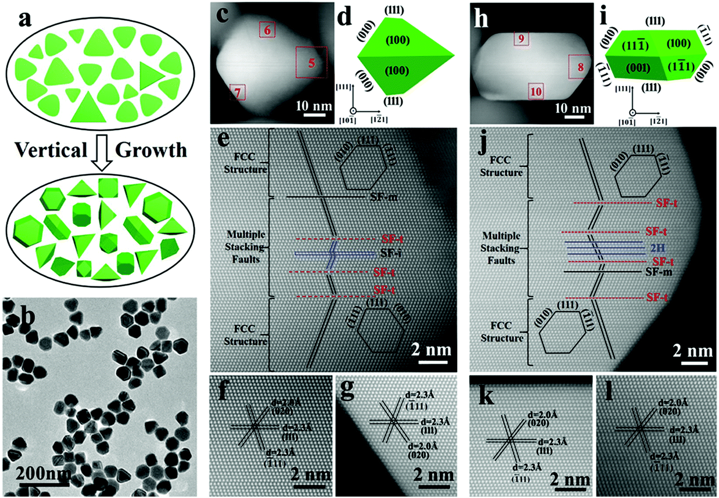 | ||
| Fig. 2 TEM analysis of nanoplates after vertical growth and crystal simulations. (a) An illustration of the vertical growth of rounded triangular nanoplates and (b) TEM image of the products after vertical growth. (c) HAADF image of a truncated bipyramid and (d) corresponding geometric model. (e), (f) and (g) HR-HAADF images of enlarged areas 5, 6 and 7 marked with a square in (c), respectively. (h) HAADF image of a hexagonal nanoplate (truncated cube) and (i) corresponding geometric model. (j), (k) and (l) HR-HAADF images of areas 8, 9 and 10 marked with a square in (h), respectively. The parallel black line indicates the traces of {11} planes. | ||
For the hexagonal shape nanoplate (Fig. 2h–j and Fig. S7†), the thickness of the planar defect is about 7.6 nm. Totally, seven stacking faults including four SF-t and four SF-m were present. Unlike the truncated bipyramid, the extending orientations of the 〈11〉 faces (area 9 (Fig. 2k) and area 10 (Fig. 2l)) remain unchanged after growth. Interestingly, three adjacent SF-m form a 2H phase as marked by blue lines in Fig. 2j. It should be mentioned here that, besides aberration-corrected TEM, traditional HRTEM (Fig. S8†) can also verify the presence of 7 stacking faults in a similar hexagonal nanoplate despite its lower resolution and incapability in differentiating the specific type of stacking faults (individual atoms).
Comparing the stacking fault structure of the original nanoplate with that after vertical growth, the thickness of the nanoplate was about 7.0 nm before growth. After growth, the thickness of layer of defect structure was maintained (∼7.5 nm). Additionally, the number of stacking faults before and after growth both fell in the range of 4 to 9, which also means that no obvious changes occur. The comparison implies that the stacking fault structure tends to remain unchanged and the formation of more stacking faults is not favored in later vertical growth.
Stacking fault structure and classification
After investigating nine nanoplates/particles, the stacking fault structures in those nine nanoplates/particles are different from each other. For some of the particles, the stacking fault structure is simple and just composed of one kind or a combination of two and/or three kinds of those basic SFs with varied numbers. The representative particles with a simple stacking fault structure are particles in Fig. 1b, c and 2c. For some other particles, composite stacking faults could be formed, such as particles in Fig. 1d containing the 4H phase and particles in Fig. 2h containing the 2H phase. In those three basic stacking faults, SF-t is different from the other two. The SF-t possesses a twinned plane and the twin plane changes the extending orientation of {11} facets (Fig. S9a†). Furthermore, when the lattice passes through two SF-t, the extending orientation of {11} facets experiences twice changes and remains unchanged (Fig. S9b†). As a result, nanoplates with an odd number and even number of SF-t are distinct from each other in different face orientations and face arrangements, which is consistent with the truncated bipyramids and hexagonal nanoplates. Therefore, we propose that the stacking fault structure in silver nanoplates could be mainly classified into four kinds (Table 1 and Fig. 3): simple stacking fault structure with an even number of SF-t, simple stacking fault structure with an odd number of SF-t, composite stacking fault structure with a 2H phase, and composite stacking fault structure with a 4H phase.
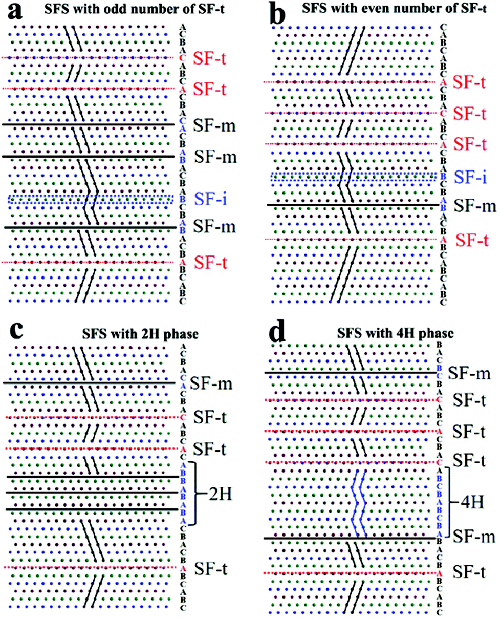 | ||
| Fig. 3 The simulated lattice arrangements of four typical kinds of stacking fault structures. Stacking fault structure with (a) an odd number of SF-t and (b) an even number of SF-t. Stacking fault structures with (c) the 2H phase and (d) 4H phase. | ||
| SFS | Compositions | Symmetry ① |
|---|---|---|
| Symmetry: the lattice symmetry along the 〈111〉 direction. | ||
| Simple | SF-m, SF-i, SF-t (odd number) | Mirror symmetry |
| SF-m, SF-i, SF-t (even number) | Center symmetry | |
| 2H phase | SF-m, SF-i, SF-t (odd number), 2H | Mirror symmetry |
| SF-m, SF-i, SF-t (even number), 2H | Center symmetry | |
| 4H phase | SF-m, SF-i, SF-t (odd number), 4H | Mirror symmetry |
| SF-m, SF-i, SF-t (even number), 4H | Center symmetry | |
In a perfect Ag fcc crystal, an improper rotation S6 exists along the 〈111〉 direction. Therefore, the Ag fcc crystal possesses center symmetry along the 〈111〉 direction. When only SF-i and/or SF-m were present in nanoplates, the center symmetry remained unchanged due to the unchanged ABCABC… order. When a single SF-t is present, a twin plane is formed and the nanoplate exhibits mirror symmetry along the 〈111〉 direction. However, while two SF-t were present, the ABCABC… order on one side of the planar defect experienced twice changes and remained unchanged on the other side of the planar defect, suggesting that nanoplates with an even number of SF-t possess center symmetry (regardless of the defect area). The symmetries of nanoplates along the 〈111〉 direction are determined by the fcc structure itself and the number of SF-t. By symmetry, therefore, silver nanoplates can be divided into two kinds: nanoplates with center symmetry and nanoplates with mirror symmetry.
The origin of 2D anisotropic growth
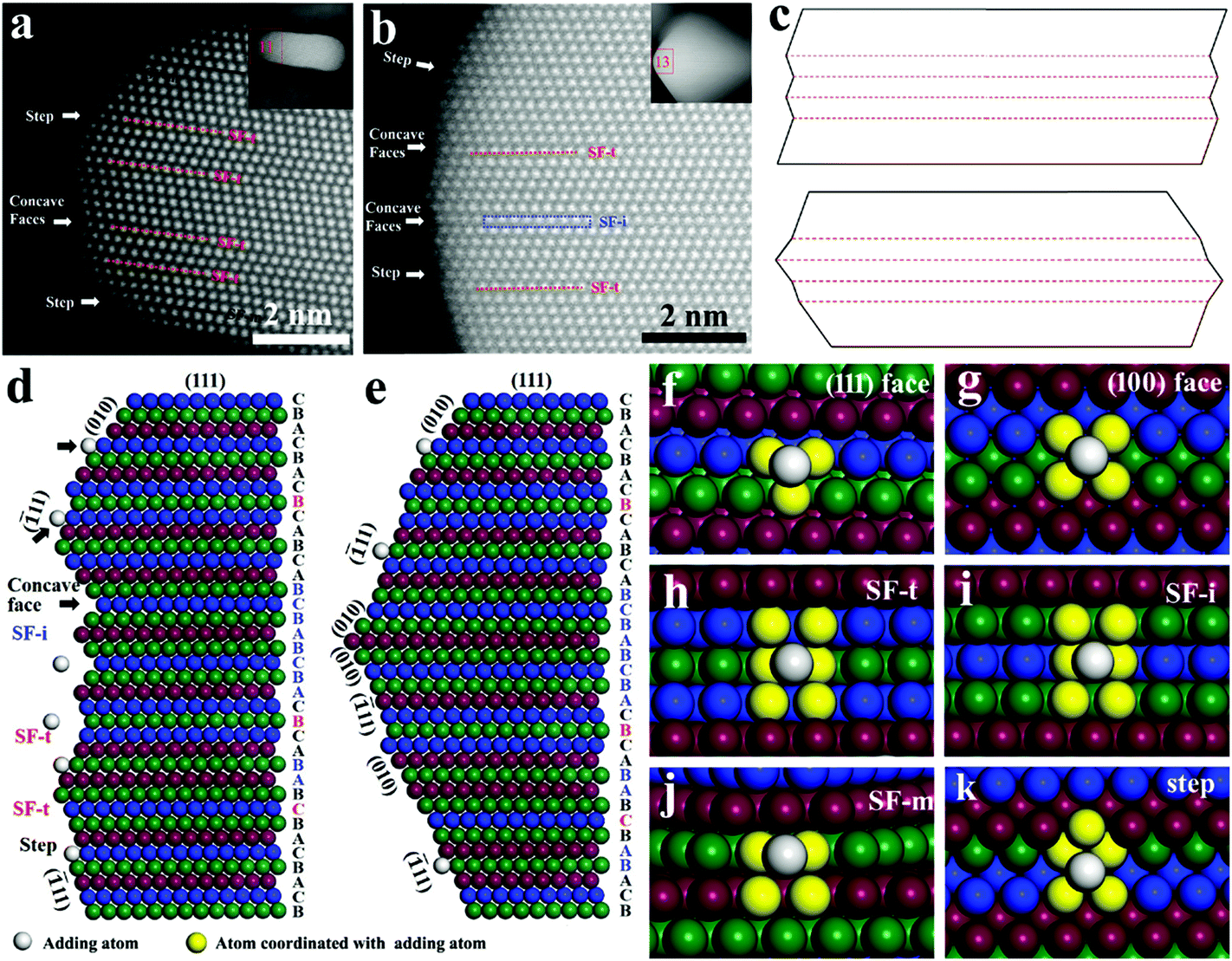
In the presence of citrate and Cu(NO3)2, the silver nanoplates (severed as seeds) could grow along the lateral direction into large triangular nanoplates with an edge length of ∼78 nm (Fig. S10a†) and ∼130 nm (Fig. S10b†) by adding 1 mL and 2 mL AgNO3 for growth, respectively (details in the ESI†). The anisotropic growth of Ag nanoplates is correlated with the stacking fault structure. Herein, the resolved stacking fault structure provides an opportunity to understand the origin of the anisotropic growth. The anisotropic growth occurs on the surface of the lateral sides, indicating that the surface structure at the defect area is the key factor. From the HAADF images shown in Fig. 4a and b, the presence of small (111) and (100) faces was observed at the surface along the lateral direction. Additionally, multiple step faces and sawtooth structures with convex and concave faces could also be found. Apparently, the formation of concave faces was correlated with the transformation of face orientation, which was induced by a twin plane such as in SF-t. For the structure of SF-i, ABC![[A with combining low line]](https://www.rsc.org/images/entities/char_0041_0332.gif)
![[B with combining low line]](https://www.rsc.org/images/entities/char_0042_0332.gif)
![[C with combining low line]](https://www.rsc.org/images/entities/char_0043_0332.gif) ABC… could be viewed as ABCABBBC… with two short twin planes, in which short concave faces with a layer of three atoms could also be formed (Fig. S11†). As a result, the formation of convex and concave faces was caused not only by SF-t (twins), but could also be caused by SF-i.
ABC… could be viewed as ABCABBBC… with two short twin planes, in which short concave faces with a layer of three atoms could also be formed (Fig. S11†). As a result, the formation of convex and concave faces was caused not only by SF-t (twins), but could also be caused by SF-i.
 | ||
| Fig. 4 Surface structure of nanoplates and structural simulations with adding atoms in the lateral growth. (a), (b) Side surface structure of rounded nanoplates and truncated bipyramids (the inserts are the corresponding nanoplates/particles). (c) Simulations of nanoplates with concave and convex faces. Simulation of growth with adding atoms on the surface of defect structure with (d) concave faces and (e) convex faces. Simulation of the surface for adding atoms with different coordination numbers on (f) the (111) face, (g) (100) face, (h) surface of SF-t, (i) surface of SF-i, (j) surface of SF-m, and (k) surface of (111) face step. | ||
The surface structure around the defect area of the nanoplate was composed of a (100) face, (111) face, step face, concave faces and convex faces. In growth, whether the (100) faces or (111) faces are dominant at the surface are determined by capping agents and growth conditions, which in turn control the surface face arrangements and surface structure. In extreme cases, there are two models of surface structure as shown in Fig. 4c: surface structure with multiple concave faces and surface structure with convex faces. The atomic arrangements on the surface of the defect structure were also simulated for the concave (Fig. 4d) and convex structures (Fig. 4e). The surface faces on the concave structure are mainly (111) faces, while on the convex structure, (111) faces and (100) faces are exposed alternatively.
For growth on nanoplates with a concave structure, the reduced Ag0 atoms are added on the faces. The coordination number of the adding atoms on the surface determines their stabilization and growth rate. On nanoplates with a concave structure as revealed in Fig. 4f–g and Fig. S12 and S13,† the coordination number for adding atoms is 3 on the (111) face and 4 on the (100) face, while at the concave sites as shown in Fig. 4h, i and Fig. S14 and S15,† the coordination number could increase up to 6 for both of SF-t and SF-i. The significantly increased coordination number leads to the enhanced stabilization of adding atoms on concave sites and results in fast deposition. The two-dimensional structure of stacking faults and the exposed defect sites in the lateral direction determine the anisotropic growth along the lateral direction. It is worth mentioning that a single concave structure in the Ag nanoplate is rather small (on the scale of sub-nanometers). The small size makes it possible that multiple concave structures could be formed with just several nanometer thicknesses, which may contribute much to the anisotropic growth. This is much different from the reentrant groove structure found in AgX (Cl or Br) on a scale of tens of nanometers.43
The concave faces grow faster than convex faces. The fast growth of concave faces would make them grow out and lead to formation of nanoplates with only convex faces left at the lateral sides as revealed in Fig. 4c (bottom). Because of the changing orientation of {11} facets, small (111) faces and (100) faces were arranged alternatingly at the surface of the defect area (Fig. 4e). The presence of SF-m would not generate a concave structure, but a site with 4 coordination number for adding atoms could be formed on the (111) face (Fig. 4j and Fig. S16†), which means that a tiny (100) face with a layer thickness of two atoms was formed. The coordination number of adding atoms on the (100) face is four and more than that of three on the (111) face. Growth on (100) faces is more favourable than on the (111) faces, especially when citrate is present and selectively adsorbed on the (111) faces. What's more, if atoms are deposited the defect sites or (100) faces and step faces (Fig. 4k and Fig. S17†) would be formed. The step faces provide sites for adding atoms with 5 coordination number, which is also more than that on flat faces. This means that once the growth starts, the anisotropic growth would remain unchanged until complete growth of a whole layer. The arrangement of (100) faces on the surface of the defect area drives the growth of nanoplates along the lateral direction. Therefore, even if no concave face is present, (100) faces are formed inevitably at the surface of the defect area, driving the anisotropic growth along the lateral direction. That explains why triangle nanoplates without concave faces could still maintain the lateral growth. It is worth mentioning that all of SF-t, SF-i and SF-m could contribute to the two-dimensional anisotropic growth of Ag nanoplates.
Shape evolution of nanoplates in vertical growth
As mentioned above, silver nanoplates were grown into truncated bipyramids and thick hexagonal nanoplates (truncated cube) in the presence of CuCl2. In order to clearly show the shape evolution process, we have utilized larger triangular nanoplates with an average edge length of 78 nm (Fig. 5a and Fig. S10a†) as seeds for vertical growth (details in the ESI†). Fig. 5 and Fig. S18–S23† show the images of growth products. With growth of 0.25 mL AgNO3 as shown in Fig. 5b and Fig. S18,† triangular nanoplates were changed into truncated triangular or hexagonal or near round nanoplates. Further increasing the amount of AgNO3 to 0.5 mL, it appears clearly that the nanoplates are divided into two kinds of morphologies: slightly truncated triangular (Fig. 5c and h) and hexagonal nanoplates (Fig. 5c and l). Along with vertical growth, increasing thickness leads to larger and larger side faces and shrinking of the top face. The morphology evolution is simulated in Fig. 5h–o. For truncated triangular nanoplates (Fig. 5h–k), the three small truncated corners grow quickly and the nanoplates grow back to triangles along with increasing thickness. Later, the triangular nanoplates grow into truncated bipyramids and eventually evolve into bipyramids (Fig. 5f and k). As to hexagonal nanoplates (Fig. 5l–o), the hexagonal shape (at the middle of nanoplates) remains unchanged during the vertical growth, but the top face shrinks. Until the top face evolves into a triangle, this hexagonal nanoplate is exactly the same shape as a truncated cube, which is revealed in Fig. 5m by viewing from different directions. In the later growth, selective growth occurred on the triangle faces, and then the hexagonal nanoplate (truncated cube) evolved into a perfect cube (Fig. 5f and o). Therefore, in the vertical growth, part of nanoplates evolve into cubes and another part into bipyramids. The ratio of bipyramids to cubes is nearly 1![[thin space (1/6-em)]](https://www.rsc.org/images/entities/char_2009.gif) :1 by measuring over 60 particles (Fig. S23†). The transformation of nanoplates to cubes and/or bipyramids is consistent with previous reports.44,45 A high-resolution (HR) TEM analysis (Fig. S24†) test confirms that the surfaces of both of cubes and bipyramids are enclosed by (100) faces. It should be noticed that at the beginning of growth, the shape of each nanoplate can exhibit as triangular, truncated triangular or hexagonal, and even rounded nanoplates, no matter the nanoplate is in center or mirror symmetry, which is also observed in gold nanoplates.46
:1 by measuring over 60 particles (Fig. S23†). The transformation of nanoplates to cubes and/or bipyramids is consistent with previous reports.44,45 A high-resolution (HR) TEM analysis (Fig. S24†) test confirms that the surfaces of both of cubes and bipyramids are enclosed by (100) faces. It should be noticed that at the beginning of growth, the shape of each nanoplate can exhibit as triangular, truncated triangular or hexagonal, and even rounded nanoplates, no matter the nanoplate is in center or mirror symmetry, which is also observed in gold nanoplates.46
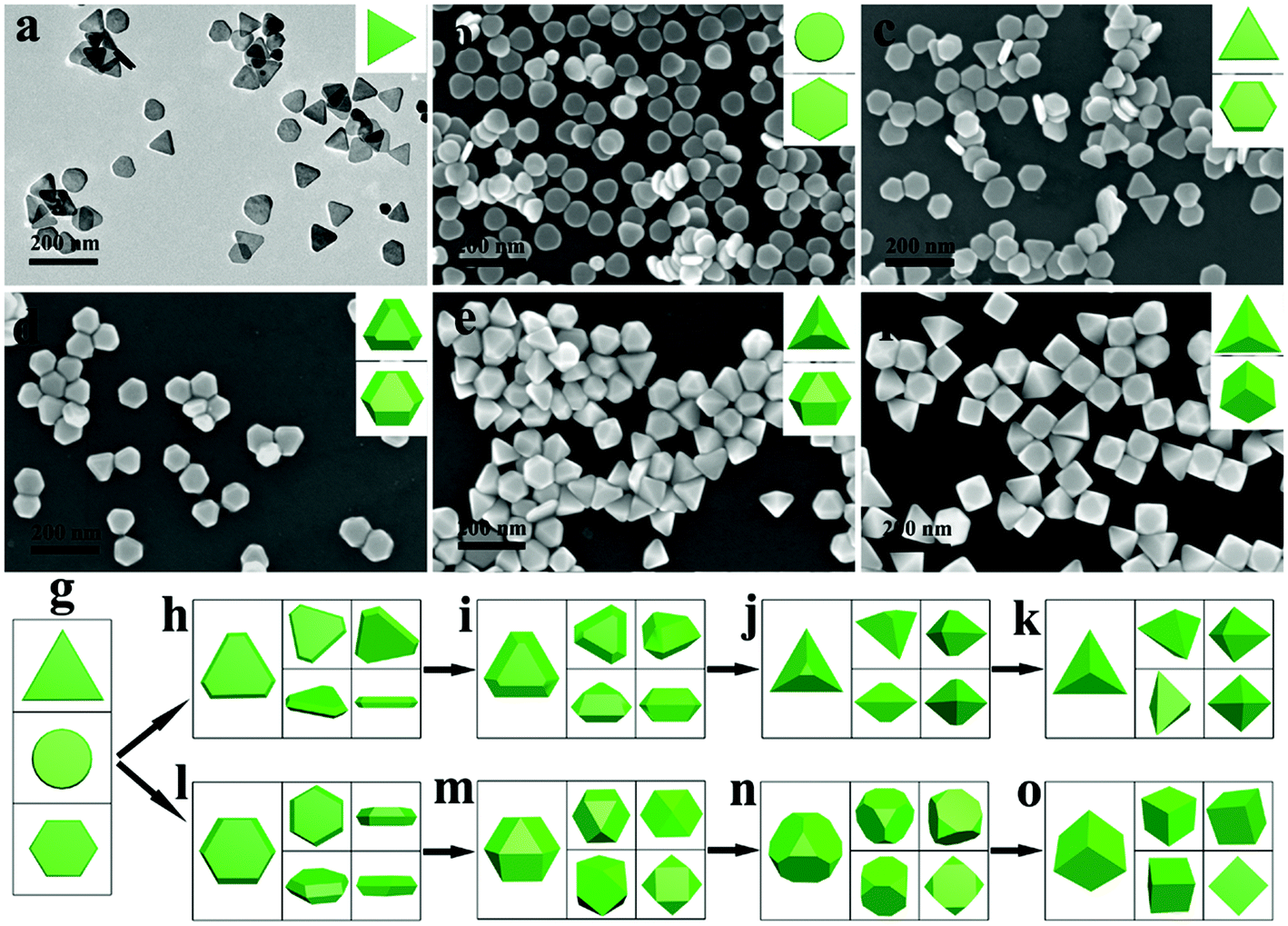 | ||
| Fig. 5 Shape evolution of nanoplates in the vertical growth. (a) TEM image of triangular nanoplates. Nanoplates or nanoparticles after growth with different amounts of AgNO3 on triangular nanoplates: (b) 0.25 mL, (c) 0.5 mL, (d) 1 mL, (e) 2 mL, and (f) 4 mL. (g) Geometric simulations of Ag nanoplates including triangular, hexagonal and round nanoplates serving as starting shapes in the evolution. (h–k) The shape evolution of truncated triangular nanoplates into bipyramids. (l–o) The shape evolution of hexagonal nanoplates into cubes. | ||
Symmetry controlled shape evolution
A question arose as to why some nanoplates would evolve into bipyramids and some grow into cubes. Both of the cube and bipyramid are evolved from nanoplates, but they possess different symmetries in shape. Apparently, the shape of the cube possesses center symmetry while the bipyramid possesses mirror symmetry along the (111) zone axis. This is consistent with the nanoplates with center symmetry and mirror symmetry. Specifically, silver nanoplates with an even number of SF-t and odd number of SF-t would exhibit center symmetry and mirror symmetry, respectively. It is rational that the symmetries of nanoplates determine the shape evolution of nanoplates with center symmetry to cubes and nanoplates with mirror symmetry to bipyramids, respectively.For simple, we take mirror symmetry nanoplates with single SF-t and center symmetry nanoplates with only SF-m as the representative two models to illustrate how symmetries control the shape evolutions. Fig. 6a shows that a nanoplate with a single SF-t possesses mirror symmetry. Along the 〈111〉 direction, the mirror symmetry determines that the sequences below and above the stacking fault are opposite to each other (ABCABC… vs. CBACBA…). For the lattice arrangement (left of Fig. 6a), the {010} facets must be arranged in mirror symmetry with one below and one above the mirror plane, which is the same for {11} facets. To minimize the surface energy, particles tend to grow into a convex polyhedron. Therefore, along the 〈2〉 direction, two (010) faces are exposed with one below and one above the SF-t. On the opposite direction 〈1![[2 with combining macron]](https://www.rsc.org/images/entities/char_0032_0304.gif) 1〉, the surface is covered by two (11) faces. Similarly, the face arrangements are the same along the 〈2〉 and 〈2〉 directions, in a manner that the side faces are arranged in mirror symmetry. The corresponding geometric simulations with face arrangements are given in Fig. 6c and Fig. S25.† In contrast, while only SF-m was formed within the nanoplate (Fig. 6b), the ABCABC… sequence remained unchanged on both sides of the stacking fault and the nanoplates exhibit center symmetry along the 〈111〉 direction (regardless of the stacking faults). According to the lattice arrangement with center symmetry, the (111) faces and (100) faces are arranged alternating with each other, which is shown in Fig. 6d and Fig. S25.† Along the 〈2〉 direction, the (010) face is below SF-m and the (11) face is above SF-m. Similarly, the (100) face and (111) face are arranged accompanying each other along the 〈2〉 and 〈2〉 directions. Therefore, there are two kinds of side face arrangements for nanoplates which is determined by their symmetries. When multiple stacking faults are present, nanoplates sill fall into center and mirror symmetry, and those two symmetries with the corresponding side face arrangements remain unchanged. The side face arrangements of nanoplates have been mentioned previously, but almost all of those research studies only have found one kind of those two.
1〉, the surface is covered by two (11) faces. Similarly, the face arrangements are the same along the 〈2〉 and 〈2〉 directions, in a manner that the side faces are arranged in mirror symmetry. The corresponding geometric simulations with face arrangements are given in Fig. 6c and Fig. S25.† In contrast, while only SF-m was formed within the nanoplate (Fig. 6b), the ABCABC… sequence remained unchanged on both sides of the stacking fault and the nanoplates exhibit center symmetry along the 〈111〉 direction (regardless of the stacking faults). According to the lattice arrangement with center symmetry, the (111) faces and (100) faces are arranged alternating with each other, which is shown in Fig. 6d and Fig. S25.† Along the 〈2〉 direction, the (010) face is below SF-m and the (11) face is above SF-m. Similarly, the (100) face and (111) face are arranged accompanying each other along the 〈2〉 and 〈2〉 directions. Therefore, there are two kinds of side face arrangements for nanoplates which is determined by their symmetries. When multiple stacking faults are present, nanoplates sill fall into center and mirror symmetry, and those two symmetries with the corresponding side face arrangements remain unchanged. The side face arrangements of nanoplates have been mentioned previously, but almost all of those research studies only have found one kind of those two.
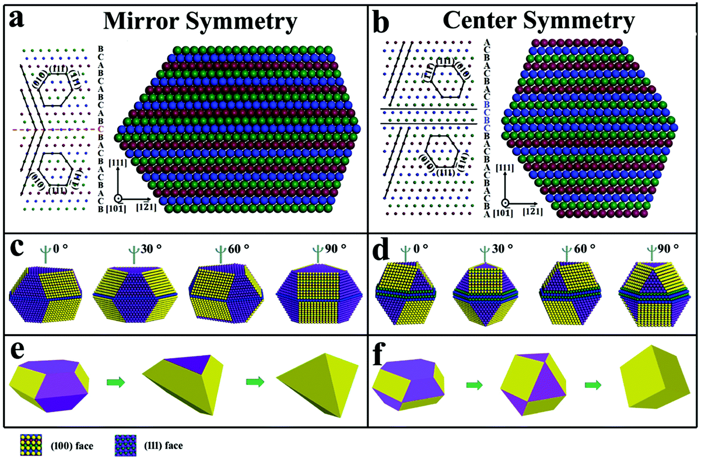 | ||
| Fig. 6 Simulation of shape evolution of hexagonal (truncated triangular) nanoplates with mirror symmetry and center symmetry in the vertical growth. (a) and (b) are hexagonal nanoplates with mirror and center symmetry along the 〈111〉 direction, respectively. (c) and (d) are the surface face arrangements of hexagonal nanoplates with mirror and center symmetry viewed from varied angles, respectively. (e) and (f) are shape evolutions of hexagonal nanoplates with mirror and center symmetry in the vertical growth, respectively. The parallel black line in (a) and (b) indicates the traces of {11} planes. | ||
The arrangement and distribution of (100) faces and (111) faces at the lateral direction play a vital role in shape evolution. In the vertical growth, the (100) faces are stabilized by the selective adsorption of Cl− and fast growth occurs on (111) faces.42 For hexagonal nanoplates with mirror symmetry (Fig. 6e), six (111) faces at the three sides would grow fast and vanish quickly, leading to only six (100) faces left at lateral sides as triangular nanoplates. With further growth along the vertical direction, the triangular nanoplates would eventually grow into bipyramids enclosed by (100) faces. As to the hexagonal nanoplates with center symmetry (Fig. 6f), the (100) face and (111) face accompanied each other at all six side edges. The suppressed growth of (100) faces would prevent the overgrowth at the six sides of hexagonal nanoplates. Fast growth on (111) faces occurs only in the vertical direction and the hexagonal shape is preserved until the formation of a truncated cube (Fig. 5 m). Finally, further overgrowth on (111) faces leads to the formation of cubes. Herein, the obtained nanocubes and nanobipyramids are actually twinned structures, which originate from that of the nanoplates. The twinned structure of nanocubes and nanobipyramids was confirmed by the selective area electron diffraction (SAED) analysis, in which two sets or even three sets of diffraction faces could be observed in a single diffraction spot (Fig. S24†). Previously, the Kitaev group47 has found that nanoplates could be transferred to cubes and bipyramids, and pointed out that the odd number and even number of twin defects of nanoplates led to the formation of bipyramids and cubes, respectively. Our work here has successfully caught the shape evolution process, and found that the symmetries with the corresponding side face arrangements induced by the twin defect (SF-t) are the key factor to manipulate the shape evolution from nanoplates to cubes and bipyramids.
Conclusion
In summary, we have systematically investigated the stacking fault structure within Ag nanoplates on the atomic level. We have found that there exist three basic stacking faults: twinned stacking fault (SF-t), a layer missed stacking fault (SF-m) and a layer inserted stacking fault (SF-i). The stacking fault structure within silver nanoplates was composed of one kind or a combination of two or three of those three stacking faults with a total number of four to nine. We have demonstrated that the origin of the anisotropic growth of nanoplates is indeed correlated with the presence of the stacking fault structure. The stacking fault structure creates concave faces, step faces and (100) faces at the surface of lateral sides. Because of the surface structure, growth along the lateral direction could be much faster than that on top and bottom (111) faces in the presence of citrate, resulting in the anisotropic growth of Ag nanoplates. It is also found that nanoplates can be divided into two kinds by symmetry: nanoplates with either center or mirror symmetry. The mirror symmetry and center symmetry of nanoplates determine the shape evolution into bipyramids and cubes, respectively. The stacking fault structure in Ag can be applied to other fcc crystals such as Au and Pd. Clearly elaborating the stacking fault structure represents an important fundamental progress in chemistry and materials science, which could enhance the understanding of origin, formation and shape evolution of two-dimensional metal nanomaterials.Experimental
Chemicals
L-Arginine, sodium borohydride (NaBH4), copper sulphate (CuSO4·5H2O), copper chloride (CuCl2·2H2O), silver nitrate (AgNO3), and ascorbic acid (AA) were purchased from Sinopharm Chemical Reagent Co. Ltd (Shanghai, China). Polyvinylpyrrolidone (PVP, Mw = 40000, reagent grade) was provided by Sigma-Aldrich. All these chemicals (analytical grade) were used as received without any further purification. Ultra-pure water (18 MΩ cm) was produced in the lab via an Ultrapure Water System.
Preparation of rounded Ag nanoplates (AgNPs)
The Ag nanoplates with high purity (over 95%) were prepared by treatment with both H2O2 and blue LED light. Detailed information could be found in previous works.19,42 Typically, in a 100 mL round-bottom flask, 2.0 mL of 25 mM sodium citrate, 0.6 mL of 2.5 mM PVP, 0.8 mL of 5 mM silver nitrate, 0.4 mL of 2 mM L-arginine and 25 mL of purified water were added and mixed together. Then the flask was immersed in an ice bath until the temperature dropped below 5 °C. Under vigorous magnetic stirring, 0.4 mL of 100 mM freshly prepared NaBH4 was injected quickly. Within about 45 min, the color of the solution changed from bright yellow to deep yellow. Subsequently, 0.4 mL hydrogen peroxide (30.0 wt%) was dropped into the solution, which produced plenty of bubbles simultaneously. Later, the colloidal solution was irradiated with a 450 nm LED light for 48 h. Finally, Ag nanoplates in high purity with a diameter of around 25 nm were prepared. For further overgrowth, the rounded Ag nanoplates were used without any purification. For electron microscopy analysis, the product was centrifuged at 6000 rpm for 20 min and washed three times using purified water.Vertical growth of rounded Ag nanoplates
In a round flask (50 mL in volume), 4.0 mL purified water, 2.0 mL rounded AgNPs, 1.0 mL of sodium citrate (25 mM), 1.0 mL of PVP (25 mM for repeat unit) and 0.5 mL of CuCl2 (25 mM) were mixed together. And then, under magnetic stirring, the flask was moved to a water bath at a temperature of 60 °C. Subsequently, 2.0 mL silver nitrate (AgNO3, 5.0 mM) and 2.0 mL ascorbic acid (AA, 5.0 mM) were simultaneously pumped into the growth solution at a rate of 12.0 mL h−1. After growth, truncated cubes and bipyramids were obtained. For electron microscopy analysis, the product was centrifuged at 3500 rpm for 20 min and washed three times using purified water.Preparation of triangular Ag nanoplates (AgNPs)
4.0 mL purified water, 2.0 mL rounded Ag nanoplates, 1.0 mL sodium citrate (25 mM) and 0.5 mL Cu(NO3)2 (25 mM) were added into a round-bottom flask in a water bath at 60 °C. Subsequently, 1.0 mL or 2.0 mL silver nitrate (AgNO3, 5.0 mM) and the same amount of ascorbic acid (AA, 5.0 mM) were simultaneously pumped into the growth solution at a rate of 12.0 mL h−1. After finishing the addition of AgNO3, two triangular AgNPs with edge lengths of 78 nm and 130 nm were yielded, respectively.Vertical growth of triangular nanoplates (78 nm)
The vertical growth of triangular nanoplates was carried out under the same conditions as vertical growth of rounded nanoplates except that the seeds and the amount of AgNO3 were different. Specifically, 2.0 mL triangular AgNPs (78 nm in length) was used, and the volumes of AgNO3 and AA solutions added into the growth solution were 0.5, 0.25, 0.5, 1.0 mL, 2.0 mL, 4.0 mL, and 6.0 mL. After the addition of silver nitrate, nanoplates with different thickness were obtained. For electron microscopy analysis, the products were centrifuged at 3500 rpm for 20 min and washed three times using purified water.Characterization
Scanning electron microscopy (SEM) images were taken on a Verios 460 L Ultrahigh Resolution Scanning Electron Microscope. Transmission electron microscopy (TEM) images, high resolution TEM images, and selective area electron diffraction (SAED) patterns were recorded on a Tian Cubed Themis G2-300 transmission electron microscope (FEI) operated at an accelerating voltage of 200 kV.Conflicts of interest
There are no conflicts to declare.Acknowledgements
This work was supported by the National Key R&D Program of China (2017YFA0700104), National Natural Science Foundation of China (NSFC) through the NSFC (21571170 and 21501168), the Fundamental Research Funds of Tianjin University of Technology and Tianjin Municipal Science and Technology Commission (20JCQNJC00450).References
- Q. Ban, T. Bai, X. Duan and J. Kong, Biomater. Sci., 2017, 5, 190–210 RSC
.
- F. Gao, G. He, H. Yin, J. Chen, Y. Liu, C. Lan, S. Zhang and B. Yang, Nanoscale, 2019, 11, 2374–2384 RSC
- Y. Zhang, F. Lv, Y. Cheng, Z. Yuan, F. Yang, C. Liu, Y. Cao, K. Zhang, H. Lu, S. Zada, S. Guo, H. Dong and X. Zhang, Adv. Healthcare Mater., 2020, 9, e1901528 CrossRef PubMed
- N. Li, H. Chen, M. Zhang, Y. Zha, Z. Mu, Y. Ma and P. Chen, Sens. Actuators, B, 2020, 315, 128135 CrossRef CAS
- X. Liu, D. Wu, Q. Chang, J. Zhou, Y. Zhang and Z. Wang, Nanoscale, 2017, 9, 15390–15396 RSC
- Y. K. Kim, G. Ok, S. W. Choi, H. Jang and D. H. Min, Nanoscale, 2017, 9, 5872–5878 RSC
- H. Mi, S. Wang, H. Yin, L. Wang, L. Mei, X. Zhu, N. Zhang and R. Jiang, Nanoscale, 2020, 12, 20250–20257 RSC
- B. Liu, J. Zhuang and G. Wei, Environ. Sci.: Nano, 2020, 7, 2195–2213 RSC
- Y. N. Wijaya, J. Kim, W. M. Choi, S. H. Park and M. H. Kim, Nanoscale, 2017, 9, 11705–11712 RSC
- A. Hwang, E. Kim, J. Moon, H. Lee, M. Lee, J. Jeong, E. K. Lim, J. Jung, T. Kang and B. Kim, ACS Appl. Mater. Interfaces, 2019, 11, 18960–18967 CrossRef CAS PubMed
- M. Maturi, E. Locatelli, I. Monaco and M. Comes Franchini, Biomater. Sci., 2019, 7, 1746–1775 RSC
- Q. Jin, M. Li, B. Polat, S. K. Paidi, A. Dai, A. Zhang, J. V. Pagaduan, I. Barman and D. H. Gracias, Angew. Chem., Int. Ed., 2017, 56, 3822–3826 CrossRef CAS PubMed
- M. Chen, S. Tang, Z. Guo, X. Wang, S. Mo, X. Huang, G. Liu and N. Zheng, Adv. Mater., 2014, 26, 8210–8216 CrossRef CAS PubMed
- H. Liu, P. Zhong, K. Liu, L. Han, H. Zheng, Y. Yin and C. Gao, Chem. Sci., 2018, 9, 398–404 RSC
- F. Muench, R. Popovitz-Biro, T. Bendikov, Y. Feldman, B. Hecker, M. Oezaslan, I. Rubinstein and A. Vaskevich, Adv. Mater., 2018, 30, e1805179 CrossRef PubMed
- H. Duan, N. Yan, R. Yu, C. R. Chang, G. Zhou, H. S. Hu, H. Rong, Z. Niu, J. Mao, H. Asakura, T. Tanaka, P. J. Dyson, J. Li and Y. Li, Nat. Commun., 2014, 5, 3093 CrossRef PubMed
- X. Chen, H. Huang, L. Pan, T. Liu and M. Niederberger, Adv. Mater., 2019, 31, e1904648 CrossRef PubMed
- N. Matsuhisa, D. Inoue, P. Zalar, H. Jin, Y. Matsuba, A. Itoh, T. Yokota, D. Hashizume and T. Someya, Nat. Mater., 2017, 16, 834–840 CrossRef CAS PubMed
- Q. Zhang, N. Li, J. Goebl, Z. Lu and Y. Yin, J. Am. Chem. Soc., 2011, 133, 18931–18939 CrossRef CAS PubMed
- Q. Zhang, Y. Hu, S. Guo, J. Goebl and Y. Yin, Nano Lett., 2010, 10, 5037–5042 CrossRef CAS PubMed
- R. Jin, Y. Cao, C. A. Mirkin, K. L. Kelly, G. C. Schatz and J. G. Zheng, Science, 2001, 294, 1901–1903 CrossRef CAS PubMed
- W. Xin, J. Severino, I. M. De Rosa, D. Yu, J. McKay, P. Ye, X. Yin, J. M. Yang, L. Carlson and S. Kodambaka, Nano Lett., 2018, 18, 1875–1881 CrossRef CAS PubMed
- M. Z. Liu, M. Leng, C. Yu, X. Wang and C. Wang, Nano Res., 2010, 3, 843–851 CrossRef CAS
- A. U. Khan, Z. Zhou, J. Krause and G. Liu, Small, 2017, 13, 1701715–1701721 CrossRef PubMed
- Y. Huang, A. R. Ferhan, Y. Gao, A. Dandapat and D. H. Kim, Nanoscale, 2014, 6, 6496–6500 RSC
- Y. Wang, H. C. Peng, J. Liu, C. Z. Huang and Y. Xia, Nano Lett., 2015, 15, 1445–1450 CrossRef CAS PubMed
- J. Roh, S. H. Back and D. J. Ahn, Small, 2016, 12, 1322–1327 CrossRef CAS PubMed
- A. J. Haes, J. Zhao, S. Zou, C. S. Own, L. D. Marks, G. C. Schatz and R. P. Van Duyne, J. Phys. Chem. B, 2005, 109, 11158–11162 CrossRef CAS PubMed
- J. E. Millstone, S. J. Hurst, G. S. Metraux, J. I. Cutler and C. A. Mirkin, Small, 2009, 5, 646–664 CrossRef CAS PubMed
- L. Chen, F. Ji, Y. Xu, L. He, Y. Mi, F. Bao, B. Sun, X. Zhang and Q. Zhang, Nano Lett., 2014, 14, 7201–7206 CrossRef CAS PubMed
- Y. Chen, Z. Fan, Z. Zhang, W. Niu, C. Li, N. Yang, B. Chen and H. Zhang, Chem. Rev., 2018, 118, 6409–6455 CrossRef CAS PubMed
- C. Lofton and W. Sigmund, Adv. Funct. Mater., 2005, 15, 1197–1208 CrossRef CAS
- J. L. Elechiguerra, J. Reyes-Gasga and M. J. Yacaman, J. Mater. Chem., 2006, 16, 3906–3919 RSC
- V. Germain, J. Li, D. Ingert, Z. L. Wang and M. P. Pileni, J. Phys. Chem. B, 2003, 107, 8717–8720 CrossRef CAS
- M. Nasilowski, B. Mahler, E. Lhuillier, S. Ithurria and B. Dubertret, Chem. Rev., 2016, 116, 10934–10982 CrossRef CAS PubMed
- D. Aherne, D. M. Ledwith, M. Gara and J. M. Kelly, Adv. Funct. Mater., 2008, 18, 2005–2016 CrossRef CAS
- T. C. R. Rocha and D. Zanchet, J. Phys. Chem. C, 2007, 111, 6989–6993 CrossRef CAS
- S. D. Golze, R. A. Hughes, S. Rouvimov, R. D. Neal, T. B. Demille and S. Neretina, Nano Lett., 2019, 19, 5653–5660 CrossRef CAS PubMed
- H. Yu, Q. Zhang, H. Liu, M. Dahl, J. B. Joo, N. Li, L. Wang and Y. Yin, ACS Nano, 2014, 8, 10252–10261 CrossRef CAS PubMed
- R. Li, S. Lu, D. Kim, S. Schonecker, J. Zhao, S. K. Kwon and L. Vitos, J. Phys.: Condens. Matter, 2016, 28, 395001 CrossRef PubMed
- J. F. Devlin, J. Phys. F: Met. Phys., 1974, 4, 1865–1882 CrossRef CAS
- T. Tan, L. Yao, H. Liu, C. Li and C. Wang, Chem. – Eur. J., 2017, 23, 10001–10006 CrossRef CAS PubMed
- G. Bögels, T. M. Pot, H. Meekes, P. Bennema and D. Bollen, Acta Crystallogr., Sect. A: Found. Crystallogr., 1997, 53, 84–94 CrossRef
- F. Ji, Q. Zhong, J. Chen, L. Chen, H. Hu, Q. Liu, P. Yang, J. Yu, L. Jiang, Y. Xu, E. Gross and Q. Zhang, Part. Part. Syst. Charact., 2018, 35, 1700114 CrossRef
- E. R. Hemesath, D. K. Schreiber, C. F. Kisielowski, A. K. Petford-Long and L. J. Lauhon, Small, 2012, 8, 1717–1724 CrossRef CAS PubMed
- F. Qin, T. Zhao, R. B. Jiang, N. N. Jiang, Q. F. Ruan, J. F. Wang, L. D. Sun, C. H. Yan and H. Q. Lin, Adv. Opt. Mater., 2016, 4, 76–85 CrossRef CAS
- M. McEachran and V. Kitaev, Chem. Commun., 2008, 44, 5737–5739 RSC
Footnote |
| † Electronic supplementary information (ESI) available. See DOI: 10.1039/d0nr06912d |
| This journal is © The Royal Society of Chemistry 2021 |