 Open Access Article
2,3-Thienoimide-ended oligothiophenes as ambipolar semiconductors for multifunctional single-layer light-emitting transistors
Mario
Prosa†
 a,
Salvatore
Moschetto†
 a,
Emilia
Benvenuti
a,
Massimo
Zambianchi
a,
Emilia
Benvenuti
a,
Massimo
Zambianchi
 b,
Michele
Muccini
 a,
Manuela
Melucci
 b and
Stefano
Toffanin
 *a
*a
aConsiglio Nazionale delle Ricerche (CNR) – Istituto per lo Studio dei Materiali Nanostrutturati (ISMN), Via P. Gobetti 101, 40129 Bologna, Italy. E-mail: stefano.toffanin@cnr.it
bConsiglio Nazionale delle Ricerche (CNR) – Istituto per la Sintesi Organica e la Fotoreattività (ISOF), Via P. Gobetti 101, 40129 Bologna, Italy
First published on 31st August 2020
Abstract
The fascinating combination of light-emitting characteristics and electrical amplification identifies organic light-emitting transistors (OLETs) as key enabling devices for a wide variety of applications, ranging from displays to sensors. Pursuing a dual functionality in a single-layer architecture is the major strength and the major challenge of this technology. Limitations mainly arise from the poor availability of organic semiconductors that are able to ensure good ambipolar behavior in charge transport together with an efficient light-emission in the solid state. In this present study, we report on a new class of thienoimide-ended oligothiophenes as molecular compounds simultaneously endowed with good field-effect mobility for holes and electrons, good processability, self-assembly capability into nanostructures and remarkable properties of photo- and electroluminescence in the solid state. The versatile chemical tuning of the molecular structure and the fine use of both solution-processed and physical deposition techniques in the realization of nanostructured thin-films are the major tools for controlling the packing of molecules and their intermolecular interactions in the solid state. Indeed, the inherent polymorphism of this class of compounds is directly correlated with their electrical and optoelectronic properties as active materials in multifunctional devices. Considering the field-effect transistor as a benchmark device platform, here we propose the extended family of thienoimide-ended oligothiophenes as a case study in virtue of (i) the solid and throughout correlation of the molecular structure and solid-state organization with the figures of merit in transistor-based devices, and (ii) the possibility of engineering highly integrated planar organic optoelectronic devices with multiple functionalities for the investigation of photophysical and charge transport processes in organic compounds and, ultimately, the demonstration of real-setting applications of OLET technology.
1. Introduction
In the last few decades, π-conjugated materials and in particular organic semiconductors (OSCs) have driven the attention of both academia and technological industry. The fascinating combination of soft processability and electronic characteristics opens the way towards the real-setting application of organic materials in highly integrated, flexible and wearable devices.1 The ease of processing on a wide range of substrates is one of the key factors of OSC expansion. In addition, the possibility to easily tune the combination of charge-carrier mobility, photonic and electroluminescence characteristics makes these materials even more appealing.2 Researchers are therefore constantly looking for new strategies that, by modifying the molecular structure, allow the development of materials with pre-defined advanced and multifunctional features.3The huge impact of OSCs in our daily life is clearly visible from the extensive presence of organic light-emitting diodes (OLEDs) in the displays market.4 Over conventional displays, organic-based ones highlight advantages such as high luminous efficiency, high brightness, fast response time, low power consumption, lightweight, etc.
In general, OLEDs are ultrathin light-emitting devices capable of generating light when an electric current passes through it. A thin organic layer, which allows generating excitons, is sandwiched between two electrodes, thus forming a vertical structure with a thickness of a few hundreds of nanometers.5,6 In order to improve the efficiency, the OLED structure has been progressively improved by the insertion of additional functional layers to guarantee selective injection and transport of charge carriers to the emission layer. Despite that, the generated light needs to pass through at least one electrode to be extracted from the device. As a result, the emission efficiency is closely related to the anode transparency, possible cavity effects and waveguiding processes.7,8
To realize more efficient and multifunctional optoelectronic systems, the scientific community focused the attention on a new device structure, the organic light emitting transistor (OLET).9,10
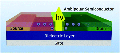
OLETs are planar field-effect devices with three terminals (source, drain and gate electrodes) that, in contrast to the vertical OLED architecture, allow the movement of the position of the emissive zone far away from any absorbing metal electrodes by the applied gate and drain voltages.11 In particular, electrons and holes can be injected simultaneously into a single ambipolar semiconducting layer and form hole and electron accumulation near the more positive and more negative electrode, respectively.9 If the semiconductor is electroluminescent, light emission is generated within the transistor channel where the opposite charge-carrier fronts meet (Fig. 1). Given that the recombination of opposite charges is mainly an in-plane diffusion of charges approaching each other, the emission region is extended by about a few microns.
This architecture integrates together the logical switching functionality of organic field-effect transistors (OFETs) and the light generation capability of OLEDs. At first glance, it is easy to understand the reason why the use of OLETs would drastically reduce the complexity of the pixel circuitry of displays. However, OLETs offer more substantial advantages that are closely linked to the architecture of the devices. Indeed, the presence of a third electrode (gate) enables a control on two perpendicularly oriented electric fields governed by the bias applied between gate–source electrodes (VGS) and drain–source electrodes (VDS). Hence, under certain conditions of bias, it is therefore possible to horizontally move the emission stripe within the transistor channel, thus reducing exciton quenching processes at the electrodes and increasing the electroluminescence quantum efficiency with respect to the OLEDs.12
Over the years, several advanced geometries have been developed in order to enhance the OLET performance,13–15 from the use of asymmetric electrodes16,17 to alternative structures such as bilayer,18–20 trilayer,12 vertical,21 OLED-separated,22 split-gate,23 overlapping gate,24etc. However, the very first step towards the complete exploitation of the OLET technology lies in the development of multifunctional OSC materials which guarantee efficient ambipolar conduction and electroluminescent emission in the solid state.
The electrically induced formation of excitons in a single organic layer is correlated with the nature of the organic compound as well as the charge transport capability of molecules in the solid state. Since the amount of emitted photons depends on the number of formed excitons, it follows that there is a direct correlation with the electron/hole current flow. The charge transport in OSCs typically occurs via hopping of charges from a molecule to another25 and it is strongly associated with the chemical structure as well as the molecular packing.26
As a result, the fabrication of efficient single-layer OLETs strongly depends on the availability of OSCs with (i) a high-charge mobility for both electrons and holes, (ii) efficient exciton formation and electroluminescence emission in the solid state and (iii) a suitably designed and controlled 3D packing of molecules propaedeutic to the former two points. Furthermore, aiming at complete exploitation of the functionalities of OLETs, accurate balancing of the electron and hole mobility is crucial to guarantee both high external quantum efficiency and throughout spatial tuning of the OLET emission region.
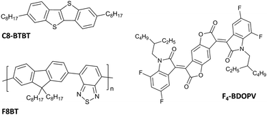
In this context, while for p-type small molecules, the mobility record is still being reset frequently (43 cm2 V−1 s−1 for C8-BTBT),27 many less n-type small molecules have been reported and the absolute mobility values are still lower when compared with the first one (12.6 cm2 V−1 s−1 for F4-BDOPV) (Fig. 2).28
The problem behind this gap mainly resides in the intermolecular interaction of molecules. When isolated molecules approach each other, the resulting valence bandwidth remains larger than the conduction bandwidth.29 This is the basic reason that explains why organic materials typically display higher hole mobilities than electron mobilities.
In an attempt to increase the electron mobility in OSCs, the introduction of strong electron-withdrawing groups such as –CN, –Cl, –F, and –CF3 and heteroatoms such as N and S was a successful strategy for the design of n-type molecules. However, when an electron is injected into the OSC, the process that occurs is similar to a chemical reduction. Hence, if the lowest unoccupied molecular orbital (LUMO) has high energy, the electron residing in the LUMO is prone to react with O2 or H2O. It follows that, over the intrinsic difficulties in obtaining good n-type behavior, molecules might also be not very stable under ambient conditions.
Apart from balanced charge ambipolarity, the other feature that must be provided by a good OSC candidate for a single-layer OLET is light emission. While charge mobility is typically favored by strong intermolecular π–π stacking, the luminescence generally decreases due to the quenching of singlet excitons.30
In recent years, the growing research of novel multifunctional materials for highly-integrated systems paved the way for new strategies of molecular engineering. Some of the remarkable approaches that have been recently introduced for tuning the OSC properties consider the chemical rigidification of the molecular structure by limiting the torsion angle, the increase of the extension of the π-conjugation, the introduction of substituents with inductive or mesomeric effects, the stabilization of the aromatic or the quinoidal resonance form, and the rational conjugation of substituted monomers to induce intermolecular order. Among the others, one of the most successful strategies for the development of multifunctional materials is to synthesize molecules or copolymers with either an electron-donor (D) or an electron-acceptor (A) moiety.31,32 While the D–A interaction regulates the strength of intermolecular π–π stacking and then the charge mobility efficiency, it is possible to decouple the light emitting function by locating the charge transfer onto the most emissive moiety or by introducing a new moiety devoted to radiative deactivation. Isoindigo,33,34 naphthalene diimide35,36 (NDI) and diketopyrrolopyrrole (DPP)37 are just some among all the electron-acceptor building-blocks used to induce n-type behavior in p-type OSCs.
To date, the milestone among emissive ambipolar materials is poly(9,9-di-n-octylfluorene-alt-benzothiadiazole) (F8BT) (Fig. 2), a green emitting D–A conjugated polymer with a photoluminescence efficiency of 50–60% in solid films.38 Due to the high electron-withdrawing capacity of the benzothiadiazole group (BT), F8BT has a high electron affinity of 3.3 eV and a large ionization potential of 5.9 eV, which allowed its use as an electron transporting layer in polymer-blend OLEDs39 and photovoltaic cells.40
When implemented in single-layer OLETs, F8BT showed well-balanced ambipolar charge transport with a saturation mobility of 7–9 × 10⁻⁴ cm2 V−1 s−1 for both electrons and holes. Due to its polymeric nature, F8BT was spin-coated onto a polymethyl methacrylate (PMMA) dielectric layer and the influence of the long-range crystalline organization on the charge mobility and EL emission zone within the channel was evident. Zaumseil et al.41 further investigated that correlation in amorphous, polycrystalline and nematic liquid crystalline F8BT films. While OLETs including an amorphous film of F8BT showed a featureless and quite narrow emission region (whose width is 2 μm), polycrystalline films led to a much broader (4 μm) emission region with the morphological presence of bright and dark spots.
If amorphous polymers are the preferential systems for optimizing the emission properties in OLETs, their (generally) low field-effect charge mobility in the amorphous phase pushed the scientific community to look for other materials. Because of the long-range order of molecular packing achievable in thermally evaporated thin films, conjugated oligomers are surely promising structures for realizing high-mobility OLETs.
In this context, major attention has been devoted in the last 10 years to thieno[2,3-c]pyrrole-4,6-diode ended oligothiophenes, better known and herein referred to as 2,3-thienoimide (TI) ended oligothiophenes, which showed a great potential as emissive ambipolar compounds endowed with easily tunable structural and optoelectronic properties.42 This class of small molecules was inspired by two widely studied analogues, the p-type α,ω-dihexyl-quaterthiophene (DH4T)43,44 and the n-type dicarbonyl ended quaterthiophene (DHCO4T),45i.e. maintaining the oligothiophene size but introducing the end substitution with the TI group. The TI substitution strategy turned out to be a powerful tool to (i) obtain electron transport, (ii) modulate ambipolarity (major p- or n-type behavior) on the basis of the number of TI groups, (iii) tune the highest occupied molecular orbital (HOMO) and the LUMO energy values, and (iv) influence the solid-state packing.46 Furthermore, unexpectedly, TI moieties promoted the light emission capability of oligothiophenes. All these features made 2,3-thienoimide oligothiophenes suitable candidates for OLET application. In addition to that, this class of OSCs showed the attractive possibility to tune the optoelectronic and photonic properties also by processing/post-synthesis treatments. Indeed, in many cases, different structural phases (polymorphs) and then different molecular organizations were observed.47 Hence, through various conventional and non-conventional deposition techniques, it was possible to obtain a specific molecular arrangement characterized by designed features.48
The combination of all these characteristics highlights the great potential of 2,3-thienoimide oligothiophenes for OLET applications. This study aims at discussing how synthetic (Section 2) and post-synthetic (Section 3) methods influence the morphological and optoelectronic properties of this class of OSCs in view of their implementation as an ambipolar emissive layer of OLETs. In Section 4, their outstanding characteristics are ultimately demonstrated to be suitable for both fundamental investigations and the development of devices with multifunctional characteristics in advanced technological applications.
2. Molecular tailoring of 2,3-thienoimide oligothiophene derivatives
Organic semiconductors based on oligothiophenes are among the most widely studied compounds for electronic and optoelectronic applications.49,50 The polarizability of sulfur atoms in the thiophene rings indeed stabilizes the conjugated backbone thus favoring the charge transport along the oligomeric backbone. In addition, oligothiophenes have unique self-assembly properties in the solid state, which make them attractive candidates for realization of nanostructured systems via non-conventional solution-processed techniques. Among the plethora of advantages, oligothiophenes are also versatile compounds because of the possibility to substitute H atoms of the thiophene rings with suitable functional groups to obtain derivatives endowed with desired physicochemical properties. The chemistry of thiophenes is well known and has been developed over the past years. They are the ideal building blocks for transition metal-catalyzed cross-coupling reactions and hence many possible strategies may be used to modify their molecular structures.51–54Oligothiophenes are widely known to be excellent p-type semiconductors. To enhance the electron transport characteristics and hence to obtain compounds having an ambipolar character, electron-withdrawing groups such as cyano groups,55 fluorinated aryls,56etc. have been introduced into the oligomer backbone to modify the frontier orbitals energy and, eventually, to increase the electron mobility. For instance, the development of perfluoroalkyl terminated quaterthiophenes57 such as DFH4T (also named as FT4F) led to OFETs with an electron mobility up to 0.24 cm2 V−1 s−1 and an unprecedented solid state optical emission efficiency when compared to the unfluorinated derivative.58 The application of DFH4T in advanced multistack OLETs allowed them to reach external quantum efficiencies exceeding 5%.12
Despite both the optical properties and the electron mobility have been effectively increased via the introduction of electron-withdrawing perfluoroalkyl moieties in oligothiophene structures, their ambipolar character and electroluminescence properties resulted to be still suboptimal.
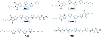
In this context, the insertion of a thienoimide group (TI or N), which is fully fused to the quaterthiophene core, emerged as an alternative and powerful approach to switch from unipolar thiophene-based materials to ambipolar and electroluminescent ones. As shown in Fig. 3, three different oligothiophenes with a single TI moiety were initially developed. While one of them comprised no other functionalization in the molecular backbone (named as T4N), the other two compounds included a hexyl or a perfluorohexyl side chain (respectively named as HT4N and FT4N). In addition, a quaterthiophene derivative endowed with two TIs (namely NT4N or T4DIM) was also synthesized (Fig. 3).
Regardless of the type of functionalization, the optical properties of all compounds in solution were found to be similar, with absorption spectra peaked at around 441–449 nm and unstructured photoluminescence spectra (Table 1). Compared to the benchmark HT4H compound, all functionalized molecules reported a slight reduction of the photoluminescence quantum yield (φ), which however resulted over 10%, except for T4N (8%). Vacuum-sublimed thin films showed a blue-shift of the optical properties with respect to the correlated solutions, thus suggesting the formation of possible polycrystalline domains in the solid state. Interesting differences were obtained in their electrochemical characteristics, especially in the resultant HOMO levels that are affected by the presence of TI units. While the presence of a single TI unit (T4N and HT4N) showed remarkable differences in the energy of the LUMO, which resulted in about 1 eV lower with respect to that of HT4H, the introduction of a second TI unit lowered the energy of the HOMO level, which resulted in −5.73 eV, −5.74 eV and −6.00 eV respectively for HT4N, T4N and NT4N (Table 1).
| OSC | λ abs [nm] | λ PL [nm] | Φ [%] | E optg [eV] | λ abs film [nm] | λ PL filmb [nm] | Φ film [%] | HOMOc [eV] | LUMOc [eV] | E g [eV] |
|---|---|---|---|---|---|---|---|---|---|---|
| a In CH2Cl2, 10−5 M. b 30 nm thick film. c E HOMO = e(4.68 − EOX°); ELUMO = e(4.68 − ERED°).59–62 d In o-chlorobenzene. e From ref. 12. f Taken from ref. 63 and corrected by CH2Cl2/H2O liquid junction. g E HOMO = e(4.37 + EOX°); ELUMO = e(4.37 + ERED°).64 | ||||||||||
| T4N | 441 | 606 | 8 | 2.81 | 344 | 603 | 1 | −5.74c | −3.47c | 2.27 |
| HT4N | 447 | 631 | 17 | 2.77 | 340 | 584/611 | 1.2 | −5.73c | −3.42c | 2.31 |
| FT4N | 433 | 580 | 11 | 2.83 | 361 | 580 | 1.8 | −5.99c | −3.42c | 2.57 |
| NT4N | 449 | 572 | 13 | 2.76 | 430 | 603 | 1.5 | −6.00c | −3.47c | 2.53 |
| NT4Nf | 451 | 568 | — | — | — | — | — | −5.69 | −3.16 | — |
| HT4H | 406d | 470, 500, 535 | 19 | 3.05 | 267, 337, 456 | 523, 562 | 0.6 | −5.5e | −2.40e | 2.87 |
| FT4F | 417 | 466, 500, 529 | 16 | 2.97 | 350, 413, 450 | 525, 563, 614 | 7 | −6.2e | −3.30e | 2.88 |
| NTE | 465 | 588 | — | — | — | — | — | −5.54 | −3.16 | 2.38 |
| NTI | 471 | 544 | — | — | — | — | — | −5.65 | −3.28 | 2.37 |
| NTA | 433 | 547 | — | — | — | — | — | −5.83 | −3.17 | 2.66 |
| NTzN | 428 | 489, 514 | — | 2.57 | — | — | — | −5.81g | −3.24g | — |
| NThTN | 443 | 546 | — | 2.49 | — | — | — | −5.69g | −3.2g | — |
| NTMeN | 449 | 581 | — | 2.39 | — | — | — | −5.65g | −3.11g | — |
| C1-NT4N | 350, 450 | 617 | 4 | — | — | — | — | — | — | — |
| C3-NT4N | 345, 429 | 605 | 6 | — | — | — | — | — | — | — |
| C6-NT4N | 346, 426 | 602 | 5 | — | — | — | — | — | — | — |
| C6cyc-Nt4N | 365, 432 | 592 | 4 | — | — | — | — | — | — | — |
| C6br-NT4N | 368, 446 | 604 | 6.5 | — | — | — | — | — | — | — |
| C8-NT4N | 345, 427 | 604 | 3.5 | — | — | — | — | — | — | — |
Interestingly, all TI-compounds reported the HOMO to be delocalized over the entire molecule, while the LUMO had high probability to be located on the TI moiety (Fig. 4). Diversely, NT4N showed a LUMO that is delocalized over the entire molecule, which is likely due to the symmetry of the structure.
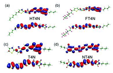 | ||
| Fig. 4 HT4N, FT4N, T4N and NT4N HOMOs (down)/LUMOs (top) orbital plots. Reprinted with permission from Chem. Mater., 2013, 25(5), 668–676. Copyright (2013) American Chemical Society. | ||
The chemical structure of the reported compounds has a critical long-range effect also in defining the electronic characteristics in the solid state. On comparing NT4N and FT4N as isolated molecules, the HOMO–LUMO positioning and energy gap were almost identical. Nevertheless, their charge mobilities were found to be drastically different and NT4N showed the best p- and n-type charge mobilities with respect to all non-symmetric compounds, i.e. 7 × 10⁻³ cm2 V−1 s−1 and 0.55 cm2 V−1 s−1 for holes and electrons, respectively. Despite further insight into the field-effect behavior of TI-ended quaterthiophenes (as discussed in Section 4), it is clear that the best candidate among TI derivatives towards the achievement of emissive ambipolar devices is represented by NT4N. For a better understanding of the origin of the ambipolar electroluminescence characteristics of NT4N, a deeper analysis on the optical features and solid-state organization is necessary. In particular, from the UV-visible optical characteristics of the molecule, a high molecular planarity and rigidity was suggested because of the similar absorption and emission spectra in both solution and film states. Nevertheless, the solvatochromic effect that the solvent can have on the optical properties of the molecule may also contribute to invariant optical spectra. In detail, as shown in Table 1 and Fig. 5b, the absorption peak was found to be located at about 450 nm and 430 nm, respectively, for the solution and film states. The emission peak was at an energy level of 572 nm in solution and 603 nm in the solid state and, similarly to other oligothiophene derivatives (Table 1), the photoluminescence quantum yield of NT4N in thin films was around 1.5%.
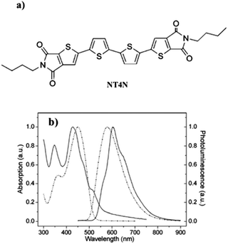 | ||
| Fig. 5 (a) Molecular structure of NT4N (b) normalized absorption and emission of NT4N solution (CH2Cl2, 4 × 10⁻⁵ M, dashed line) and film (100 nm thick, solid line). Adapted from ref. 63 with permission from the Royal Society of Chemistry. | ||
From a crystallographic point of view, the molecular backbone of NT4N was found to be almost planar as a consequence of the two coplanar inner thiophene rings and a dihedral angle of only 4.4° between the inner thiophenes and the thiophene-imide units (Fig. 6a). The crystal packing of NT4N molecules was indeed different from the typical herringbone structure of oligothiophenes and consisted of a slipped π–π stacking packing mode with an interplanar distance of about 3.51 Å in which the molecules slide along the long molecular axis of 3.32 Å (Fig. 6b).65
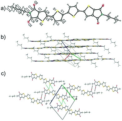 | ||
| Fig. 6 (a) ORTEP drawing of NT4N (b) crystal packing of π–π stacks in arbitrary view (c) view along the 1D supramolecular network axis generated by C–H⋯O interactions (dashed black). S⋯S and C–H⋯S contacts (light blue). Reproduced from ref. 63 with permission from the Royal Society of Chemistry. | ||
In detail, the intermolecular C–H⋯O H bonds between two oxygen in anti-position and one hydrogen, that is attached to the imide-carbon atom of two different molecules, formed a 1D supramolecular organization constituted by molecules of adjacent π–π stacks (Fig. 6c). In addition, the sulfur atoms of the fused imidothiophene rings had intermolecular interactions with (i) the hydrogens of the inner thiophene rings and (ii) sulfur atoms of the fused imidothiophene rings, which were not involved in the C–H⋯O interactions, of neighboring molecules (Fig. 6c).66 By following the process of thin film formation, a layer by layer growth mechanism resulted in a bidimensional surface morphology with an almost perpendicular arrangement of NT4N molecules with respect to the substrate.
As a result of the symmetric and planar structure, the formation of π-stacks of NT4N molecules showed remarkable differences from the herringbone-like crystal packing of FT4N.67 This may be the enabling factor for the excellent electrical characteristics of NT4N, which strongly differs from the other quaterthiophene derivatives (Table 1). The particular organization of NT4N molecules may also induce a possible reduction of non-radiative exciton paths. Indeed, despite the NT4N photoluminescent quantum yield in thin-film not being as high as that of other compounds, the corresponding single-layer ambipolar OLETs showed an optical power unexpectedly high (hundreds of nW) for this category of conjugated organic semiconductors.
Over the years, major attention has been devoted to the tentative optimization of NT4N and the synthesis of similar chemical structures for the development of efficient ambipolar OLET devices.
This approach paved the way for the development of an entire class of TI derivatives, thus allowing the understanding of the correlation between the molecular structure, molecular packing and optoelectronic performance. A schematic representation of the various synthetic strategies to modify the NT4N prototype molecule is shown in Fig. 7 and selected examples of each approach are deeply described below.
As a method to perturbate the π-conjugated system of NT4N and to ultimately tune the optoelectronic and packing properties, Zambianchi et al. inserted different unsaturated bridges between the two thiophenes of the inner core.68 In particular, ethylene, azomethine and ethinyl (or acetylenic) inner bridges were inserted into 2,3-thieno(bis)imide ended oligothiophenes, namely NTE, NTI and NTA, respectively (Fig. 8a). While ethylene and azomethine bridges were used to enhance the molecular planarity and reduce the optical band gap, the main effect expected from the acetylenic bridge was an increase in the band gap originating from the mismatch of the sp carbon orbitals with the π-delocalized system. Accordingly, spectroscopic characterization showed an absorption band strongly red-shifted for NTE (465 nm) and NTI (471 nm) while a blue-shift was evidenced for NTA (433 nm) when compared to NT4N (451 nm) (Table 1). Regarding the emission properties, NTE reported a spectrum largely red-shifted with respect to the other compounds. Nevertheless, the photoluminescence quantum efficiency (φ) measured in solution was found to be comparable for NTE (19%) and NTA (20%) and also similar to that of NT4N (13%, Table 1), while a relatively low φ was obtained from NTI (2%).
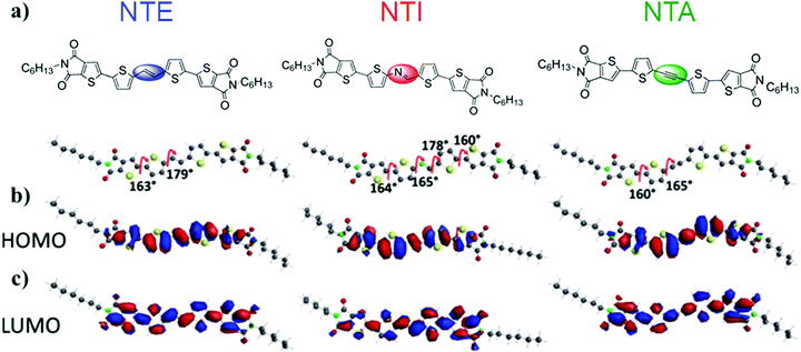 | ||
| Fig. 8 (a) Chemical structures of the NT4N-derivatives NTE, NTI and NTA, which respectively include ethylene (blue), azomethine (red) and ethinyl (green) inner bridges between the two thiophene inner cores (b) NTE, NTI and NTA HOMO plots (c) NTE, NTI and NTA LUMO plots. Adapted from ref. 68 with permission from the Royal Society of Chemistry. | ||
The molecular energy levels investigated via cyclic voltammetry (CV) and computational calculations showed a comparable LUMO energy of NTA and NTE. In comparison, the LUMO energy of NTI was 0.1 eV lower than NTA's and NTE's due to the electron withdrawing effect of azomethine. Instead, the HOMO levels decreased in the order NTE > NTI > NTA thus evidencing an optical energy gap of NTA that was significantly larger than that of NTI and NTE (Table 1). To note, while the use of ethylene (NTE) mainly enhanced the HOMO level of 0.1 eV with respect to NT4N, the introduction of azomethine (NTI) reduced the LUMO level of 0.1 eV. Hence, both NTE and NTI showed optical energy gaps (about 2.4 eV) that were similarly lower than that of NT4N (2.53 eV).
From a conformational point of view, all molecules were almost planar, with dihedral angles between the inner thiophene and the TI moiety of 160° and between the inner thiophene and the additional inner bridge of 180° and 165° respectively for NTE and NTA. According to what was observed for NT4N, the HOMO orbital of NTE and NTA was homogeneously distributed over the inner thiophene cores with extended LUMO orbital distribution to the TI units. Diversely, the lack of a center of symmetry in the NTI molecular structure due to the azomethine inner bridge resulted in a high probability of LUMO mainly localized on the thienoimide inner bridge (Fig. 8b).
As a further step to the inner core modification of NT4N, Durso et al. reported on the substitution of the bithiophene (TT) π-inner core with bithiazole and thienothiophene fused rings, which are moieties respectively and are more electron-deficient compared to TT.46 The newly synthesized compounds aimed at improving the ambipolar characteristics of NT4N. Indeed, while thiazole rings are expected to improve the electron charge transport behavior, the use of thienothiophene is associated with an enhanced hole charge transport as demonstrated in the case of linear oligothiophenes.69 In detail, the new compound including the bithiazole core was named as NTzN, while the second one with thienothiophene was named as NThTN. A further derivative was synthesized by inserting electron rich methyl substituents into the two thiophene inner cores of NT4N (NTMeN) (Fig. 9a).
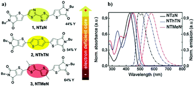 | ||
| Fig. 9 (a) Molecular structures of NT4N derivatives in which the TT inner core is substituted by bithiazole (NTzN), thienothiophene (NThTN) or an additional methyl substituent is inserted in each of the two TT thiophenes (b) absorption and emission spectra of NTzN, NThTN and NTMeN in solutions. Adapted from ref. 46 with permission from the Royal Society of Chemistry. | ||
The UV-Vis optical absorption and emission spectra in solutions were found to be progressively more blue-shifted as the electron-deficiency of the inner-cores increased (Fig. 9b). In particular, the presence of the bithiazole core shifted the absorption peak of about 15 nm and 21 nm with respect to NThTN and NTMeN (Table 1). Accordingly, the optical band of NTzN was about 0.1 eV and 0.2 eV lower than that of NThTN and NTMeN, respectively.
Interestingly, the energy of both frontiers orbitals increased in the order NTzN > NThTN > NTMeN, with a different magnitude of variation between the HOMO and the LUMO. Computational analyses confirmed that while in NTzN both the HOMO and the LUMO were delocalized over the entire molecular backbone, in NThTN and NTMeN the HOMO was localized in the inner core and the LUMO was localized in correspondence with TI moieties.
Electrical characterization performed on bottom gate-top contacts OFET devices revealed that NTzN had exclusively n-type charge transport with an electron mobility μe = 0.16 cm2 V−1 s−1, while NThTN and NTMeN showed ambipolar behavior. In particular, NThTN showed an excellent electron charge mobility μe = 0.3 cm2 V−1 s−1 and hole charge mobility μh = 6.4 × 10⁻⁵ cm2 V−1 s−1. Diversely, the more electron rich core of NTMeN led to a reduction of the electron mobility of about four orders of magnitude with respect to NTzN and NThTN and a relatively low hole mobility μh = 3.0 × 10⁻⁶ cm2 V−1 s−1.
It is clear that the modification of the NT4N inner cores generally has a direct impact on the optoelectronic properties. Despite the ambipolar charge transport not being improved with respect to NT4N, important perspectives were provided to improve the electron mobility values through the molecular tailoring of TI-derivatives.
A further optimization of the NT4N figures-of-merit was pursued with the modification of the end-substituents of the molecular structure. In this regard, by holding the same π-conjugated backbone, length and core type, and by avoiding the perturbation of the backbone electronic characteristics, different alkyl end substituents (Cx) were inserted for a selective modulation of the optoelectronic characteristics due to the different solid state organization.70 In particular, linear (C1–C8), branched (C6br) or cyclic (C6cyc) alkyl end substituents of the TI units were investigated (Fig. 10). It is worth reminding that the NT4N compound is endowed with a C4 alkyl chain and hence it is also labeled as C4-NT4N.
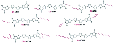 | ||
| Fig. 10 Molecular structures of NT4N derivatives including different alkyl end substituents in the TI moiety. Reproduced from ref. 42 with permission from the Royal Society of Chemistry. | ||
As expected, all compounds showed similar optical characteristics with absorption spectra of thin films mainly located at around 345 nm and 430 nm, and the emission spectra peaked at around 603 nm (Table 1).
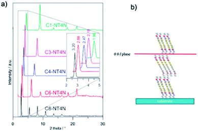
Since the substitution of the TI moieties was explored as a strategy to change the solid state organization towards their effective application in electroluminescent devices, X-ray-diffraction (XRD) patterns of the NT4N-derivatives were directly measured on the active layers in OLET devices. As shown in Fig. 11a, a strong preferential orientation with respect to the substrate was highlighted in a similar way for all molecules. In detail, each molecule exhibited a high intensity 001 reflection and additional sharp reflections that represented further orders of the interlayer distance that progressively increased with the length of the TI alkyl substituents. As shown in Fig. 11b, all NT4N derivatives were similarly arranged in the upright position with respect to the substrate as already suggested by the crystal packing of C4-NT4N (Fig. 6c).
 | ||
| Fig. 11 (a) XRD patterns of linear C1–C8-NT4N devices exposed to X-ray beam (b) molecular arrangement of Cx-NT4N. Reproduced from ref. 42 with permission from the Royal Society of Chemistry. | ||
The investigation of the electrical characteristics revealed low performance in the case of C6cyc-NT4N and ambipolar charge mobility for the linear alkyl tail (C1–C8-NT4N). In the latter case, a slight unbalancing towards the electron conduction was observed for the benchmark C4-NT4N. In detail, the hole mobility (μh) oscillated between 2 and 3.5 orders of magnitude lower than electron mobility (ranging between 0.17 and 0.32 cm2 V−1 s−1). Interestingly, C8-NT4N showed the most balanced ambipolar charge transport characteristics. Despite significant variations in thin-film structural arrangement and charge mobility not being observed among NT4N-derivatives, a slight increase of the electroluminescence intensity was reported on the increasing tail length from C3 to C8. In view of OLET applications, a defined role of alkyl end substitution of the TI moiety was evidenced in preserving and increasing the inter-layer order along the direction perpendicular to the flowing-charge plane, as clearly demonstrated by the superior performance of C8-NT4N. A more in-depth discussion of the optoelectronic performance of NT4N-based OLETs can be found in Section 4.
3. Correlation between polymorphism and optoelectronic properties in 2,3-thienoimide oligothiophenes
Over the last few years, the study of polymorphism has been the object of intense research for its key role in controlling the characteristics of organic compounds. Achieving control of polymorphism is however crucial not only for tuning the properties of molecular and polymeric solids, but also for their direct impact on the functional properties of optoelectronic devices. The optical and charge transport properties of organic devices indeed rely on the structure–property relationship of molecules, as discussed in the previous section, as well as on the modality of the molecules arranged in 2D and 3D. Typically, great attention in the design of new compounds is devoted to the correlation between functional groups and electronic properties of isolated molecules. Nevertheless, the packing of molecules and their intermolecular interactions are fundamental for the solid state characteristics. If considering the plethora of factors influencing the solid state morphology and the difficulty to control the crystal structure, it follows that polymorphism is a critical phenomenon to be accurately considered in optimizing the device performance and its reproducibility.Methods to control polymorphism in TI-ended oligothiophenes will be hereafter presented and analyzed including a chemically driven approach, such as the chemical design, or a post-synthetic one, in which processing, nucleation modality, crystallization kinetics, post-deposition treatments and crystallization in confinement will be discussed. The relevant impact of polymorphism of such compounds on device (especially field-effect transistor) performance will be also elucidated.
Chemically driven control of conformational polymorphism
The molecular packing is known to be strongly dependent on the type and the number of interactions occurring among molecules. As shown in the previous section, the chemical structure of a compound has a critical role in defining the molecular orientation in the solid state. It is therefore clear that the solid state organization and hence the formation of different polymorphs may be induced by playing on the chemistry of the molecule. In this paragraph, the obtainment of different crystal phases via chemical tuning will be discussed by analyzing some of the oligomers already examined in the previous section. As shown in Fig. 7, TI-ended oligothiophenes can be modified at different sites of the oligomer, either in the inner core or in the TI terminations. The insertion of a different saturation degree, specifically ethylene, azomethine and ethinyl (acetylenic) inner bridges, in 2,3-thieno(bis)imide ended oligothiophenes led respectively to NTA, NTE and NTI (Fig. 8a and 12). Interestingly, the deposition of the three compounds from a toluene solution onto a flat substrate led to the formation of different large crystals in the presence of concomitant polymorphs for each molecule.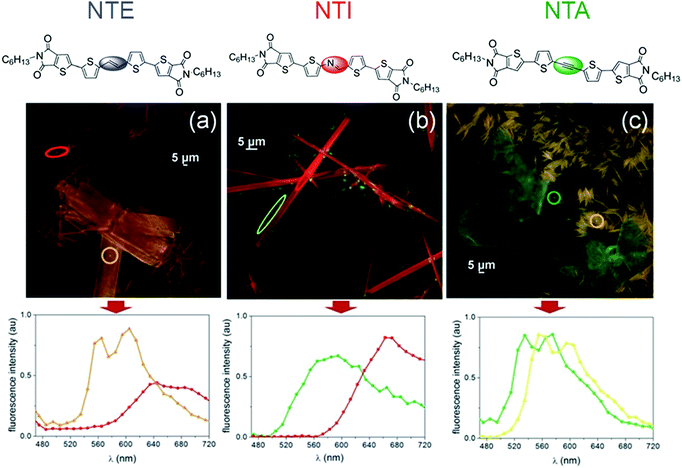 | ||
| Fig. 12 Fluorescence confocal images of films of (a) NTE (b) NTI and (c) NTA. The films were obtained upon evaporation of 0.5 mg mL−1 toluene solution on glass. Bottom: Confocal fluorescence spectra of respective compounds. Adapted from ref. 68 with permission from the Royal Society of Chemistry. | ||
More specifically, NTE formed a mixture of rod-like (red emitting, λEM = 640 nm) and platelet-like (orange emitting, λEM = 560 nm and 600 nm) polymorphs as shown in Fig. 12a, in which rod-like crystals were up-to-100 μm long while presenting widths ranging from to 5 μm to 10 μm. Diversely, platelet-like crystals showed a regular shape with a long axis ranging from 20 μm to 100 μm. The authors also highlighted the role of the initial solution in the formation of the polymorph: rod-like structures were gradually induced upon increasing the concentration.
NTI deposits showed randomly-distributed crystals with a needle shape which were characterized by a width ranging from 10 μm to 100 μm and an aspect ratio between 1![[thin space (1/6-em)]](https://www.rsc.org/images/entities/char_2009.gif) :
:![[thin space (1/6-em)]](https://www.rsc.org/images/entities/char_2009.gif) 5 and 1
5 and 1![[thin space (1/6-em)]](https://www.rsc.org/images/entities/char_2009.gif) :
:![[thin space (1/6-em)]](https://www.rsc.org/images/entities/char_2009.gif) 50. A photoluminescence emission peaked at 660 nm was concomitant to a green signal arising from small aggregates (<2 μm) decorating the rod-like crystals.
50. A photoluminescence emission peaked at 660 nm was concomitant to a green signal arising from small aggregates (<2 μm) decorating the rod-like crystals.
Despite polymorphs generated by NTE being clearly different from those of NTI, in all cases single crystals (or iso-oriented domains) were visible under polarized optical microscopy. Diversely, the deposition of NTA gave rise both to fiber-like and rhombohedral polymorphs which were respectively characterized by optical anisotropy and a polycrystalline nature (Fig. 12c).
Nevertheless, NTA reported a photoluminescence quantum yield similar to that of NTE (10% and 6%, respectively). In contrast, NTI showed a reduced yield of only 4%.
A remarkable impact of the molecular structure on the polymorph formation and correlated optical proprieties was found out. This pushed the authors to dig deep into the origin of the observed polymorphism. Independent of the molecular structure, computational simulations reported minima of energy upon the rotation of the dihedral angle between the TI moiety and the inner thiophene. More specifically, ANTI and SYN conformers were confirmed as possible crystallized polymorphs. Furthermore, the crucial role of the chemical structure was even more clear from the analysis of the frontiers orbitals overlap between molecules. With respect to the benchmark NT4N, a reduced orbital overlap was found for both frontier orbitals, with particular impact on the LUMOs. This information is relevant in assessing possible synthetic route for improving the optoelectronic performance in TI-oligothiophene based OLETs.
We have already shown in the previous section how the optical and charge transport properties of NT4N-derivatives in the solid state depend on TI substituents. Accordingly, Maini et al. further demonstrated that the conformational polymorphism of this class of compounds can be controlled by modifying the alkyl end symmetry of TI moieties.71
In detail, the use of an even number of carbons in the TI alkyl substituents revealed two possible polymorphic forms with different packing types and molecular conformations. Indeed, while the inner thiophene rings are always arranged in anti conformation, the thienoimide moieties can adopt both syn and anti conformation with respect to the inner thiophenes (Fig. 13a).
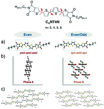 | ||
| Fig. 13 (a) Molecular conformation of Cx-NT4N and the correlated (b) view parallel to main molecular plane (c) view normal to the main molecular plane. Adapted from ref. 71 and 72 with permission from the Royal Society of Chemistry. | ||
As a result, two polymorphs can exist, that are in the conformation anti–anti–anti and syn–anti–syn. The two polymorphs adopt two different molecular packaging, in which the Cx-NT4N molecules are piled in columnar stacks with strong π–π vertical interactions (phase A) or molecules interact in a brick wall arrangement. In the latter, a molecule interacts with four different close molecules and the packing results in a lower degree of interdigitation of the alkyl chains (phase B) (Fig. 13b and c).72 Interestingly, NT4N including odd alkyl substituents in TIs displayed exclusively syn–anti–syn conformation and B-type packaging. Diversely, the use of even alkyl substituents in TIs allowed the conformational polymorphism of NT4N. A more detailed discussion of the crystal structures is reported in ref. 72. Despite the chemical structure being proved to enable conformational polymorphism, it is worth mentioning that only the phase B conformation was reported by thermal sublimation of NT4N derivatives. The control on polymorphs in the solid-state can be indeed operated by addressing suitable deposition techniques, as we will highlight in the next paragraph.
Polymorph control by post-synthesis physical methods
Aside from the nature of the chemical compound, a wide variety of post-synthesis factors can further influence the molecular packing in the solid state and hence the formation of possible polymorphs. Processing, crystallization confinement, and post-deposition treatments are some among all possible methodologies which control polymorphism.For instance, crystal phases of core-modified (NTE, NTA and NTI)68 and terminal-modified (Cx-NT4N)72 oligothiophene derivatives showed relevant transitions upon thermal heating.73 While platelet-like crystals of NTE (Fig. 12a) were persistent till the melting point, rod-like crystals showed an irreversible change of the emission from red to orange (corresponding to the emission of platelet-like crystals) without variation of the morphology after the heating cycle “room temperature (RT) → 200 °C → RT”. Under the same treatment, NTA fiber-like crystals shifted irreversibly from a yellow to a green emission, while the rhombohedral crystals remained almost unaltered. Diversely, NTI crystals did not show detectable differences in the fluorescence upon thermal treatment.
The same analysis on C4-NT4N showed an initial preferred formation of phase A at room temperature (Fig. 14), which underwent the transition to phase B upon thermal treatment.
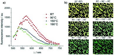 | ||
| Fig. 14 (a) Evolution of the confocal photoluminescence spectrum upon thermal treatment (b) evolution of the fluorescence in patterned film recorded by a CCD versus the temperature. The images by Gentili et al. are licensed under CC BY-NC-ND 3.0/adapted from original (ref. 74). | ||
The dependence of photophysical properties on the temperature was initially considered as a drawback for the application of such compounds in OFETs, OLEDs, OLETs, etc. Nonetheless, the thermal control of polymorphs was then exploited as a tool to record the thermal history of the system.68 Gentili et al.74 successfully fabricated a real-time temperature integrator (TTI) device, in which the quantification of the red, green and blue fluorescence components allowed the evaluation of the current temperature sensed by the crystal.
In particular, a derivative of NT4N comprising a single thiophene inner core (named as NT3N) exhibited an irreversible change of the solid state photoluminescence, passing from yellow (β polymorph) to green (α polymorph), upon heating to 190 °C for 30 seconds (Fig. 14a). This time–temperature functionality was combined with information storage capabilities of a logical matrix with micro-meter sized pixels in order to allow time–temperature information to be detected by using a conventional optical microscope (Fig. 14b).
Post-synthesis methods influencing polymorphism include all processes involved in the solid state formation. Dissolving solvents, kinetic and techniques of deposition, confinement and templating environments, are just some factors that control the formation of polymorphs.
The use of a confined environment during the crystallization process is a method particularly appealing for the proven possibility to accurately select the desired polymorph. In this regard, auxiliary solvent-based sublimation-aided nanostructuring (ASB-SANS) has been recently proposed as a new and simple method which eliminates the issue of separating the polymorph from the matrix.75 This fascinating approach exploits a material sublimating under ambient conditions to form mesocavities in which the compound of interest precipitates (Fig. 15). More specifically, both materials are typically drop cast onto a substrate and, when the solvent shrinks, the sublimating compound first precipitates thus giving rise to 3D cavities. These act as a template for the precipitation of the compound of interest, which occurs under quasi-equilibrium and confinement conditions. In this process, the molecular diffusion is typically limited and the number of nuclei of crystallization is reduced thus favoring the growth of the mean size of the crystalline domains. It follows that different polymorphs are selected on the basis of their different critical nuclei sizes.
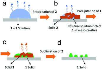 | ||
| Fig. 15 Scheme of principles of operation of auxiliary solvent based sublimation-aided nanostructuring (ASB-SANS). (a) Drop casting of 1 + 2 solution; (b) precipitation of the overabundant 2; (c) precipitation of 1 into the cavities of 2; (d) sublimation of 2. Reproduced from ref. 75 with permission from the Royal Society of Chemistry. | ||
The sublimating compound is finally sublimated away. Despite the fact that NT3N is known to form α and β polymorphs (Fig. 14), the use of ASB-SANS allowed only phase α to appear. Interestingly, the full selectivity of one phase was obtained independent of the dissolving solvent, i.e. chloroform or toluene. However, other deposition techniques influence the process of solid state formation on the basis of the solvent used to dissolve the compound. The selection of the dissolving solvent is therefore crucial for polymorphism control. In addition to that, the deposition process induces itself different kinetics of crystallization. Hence, aiming at fabricating multifunctional devices such as OLETs with reproducible and outstanding performance, the combination of all elements involved in the solid state formation needs to be carefully considered.
In this regard, Benvenuti et al. reported on the correlation between the type of deposition method and OFET characteristics, as a result of the diversely induced molecular packing.48 Thermal sublimation and supersonic molecular beam deposition (SuMBD) were used as vacuum-based approaches for preparing thin films compatible with the fabrication of field-effect transistors, while lithographically controlled wetting (LCW) was used as a solution-deposition technique able to manipulate the growth of microstructured films.76 Two different rates of deposition for both thermal sublimation and SuMBD were used for depositing C4-NT4N. Interestingly, the rate of deposition (0.1 Å s−1 and 0.017 Å s−1) of thermal sublimation did not substantially affect the resulting film, which was composed by phase B. Diversely, the deposition with SuMDB revealed a dependence of the polymorphic phase on the deposition rate, with the consequent obtainment of either phase B and a new phase called C, by respectively using a rate of 0.1 Å s−1 and 0.017 Å s−1 (Table 2).
| Deposition method | Rate [Å s−1] solvent | Phase | μ e [cm2 V−1 s−1] | μ h [cm2 V−1 s−1] |
|---|---|---|---|---|
| a C4-NT4N films. b C6-NT4N films. | ||||
| Sublimationa | 0.1 | B | 4.5 × 10⁻² | 6.7 × 10⁻⁴ |
| Sublimationa | 0.017 | B | 1.2 × 10⁻² | 1.3 × 10⁻⁴ |
| SuMBDa | 0.1 | B | 1.2 × 10⁻⁵ | 2.2 × 10⁻⁶ |
| SuMBDa | 0.017 | C | 1.3 × 10⁻⁴ | — |
| LCWb | Anisole | B | 2.4 × 10⁻³ | 1.0 × 10⁻⁵ |
| LCWb | 1,2-DCB | B (A) | 4.4 × 10⁻⁴ | 2.7 × 10⁻⁵ |
The morphologic differences between films deposited by the two techniques had an impact on the ambipolar characteristics of OFETs, in which charge mobilities resulted around 10−2 cm2 V−1 s−1 (electron) and 10−4 cm2 V−1 s−1 (hole) in thermal sublimated samples, while 1.2 × 10⁻⁵ cm2 V−1 s−1 (electron) and 2.2 × 10⁻⁶ cm2 V−1 s−1 (hole) in the sample deposited by SuMBD at 0.1 Å s−1 (Table 2). To note, the phase C obtained from the SuMBD deposition at lower rates did not show ambipolar OFET behavior, and only an n-type mobility of about 10−4 cm2 V−1 s−1 was measured.
Concerning LCW deposition, two different C6-NT4N films were deposited using an anisole solution at 80 °C and 1,2-dichlorobenzene (1,2-DCB) at room temperature.48 While the presence of phase B was found using anisole, in films deposited from 1,2-DCB the coexistence of both phase A and phase B was reported. As discussed in regard of time temperature sensors, the typical stable phase of C6-NT4N at room temperature is phase A.71 According to that, it is likely that the formation of phase B from anisole was due to the use of 80 °C as the deposition temperature. In contrast, the coexistence of both phase A and B in C6-NT4N films from 1,2-DCB solution at room temperature was ascribed to the special confinement effect of the LCW technique, which was responsible for the formation of phase B. Eventually, all films obtained from LCW deposition confirmed the typical ambipolar behavior expected from C6-NT4N, with slightly lower values of charge mobility by using 1,2-DCB as a result of the presence of phase A (electron and hole mobilities were respectively 2.4 × 10⁻³ cm2 V−1 s−1 and 1.0 × 10⁻⁵ cm2 V−1 s−1 from anisole solution and 4.4 × 10⁻³ cm2 V−1 s−1 and 2.7 × 10⁻⁵ cm2 V−1 s−1 by using 1,2-DCB) (Table 2).
4. Single layer ambipolar OLETs
The possibility to combine high flowing current densities and radiative exciton recombination (occurring far from electrodes) represents a fascinating characteristic which identifies OLETs as optoelectronic devices endowed with theoretically high brightness. Obtaining light-emission from an electrical switching and amplifying device is the major strength of the OLET platform. However, pursuing a dual functionality in a single architecture is also the major challenge of this technology. The OLET semiconducting layer indeed needs to ensure similar and high field-effect mobility of holes and electrons (ambipolarity) as well as to allow the radiative recombination of opposite charge carriers in an efficient way. In 15 years of research, a multitude of materials have been employed as ambipolar emissive semiconductors, ranging from organic to inorganic and hybrid ones.77 In this regard, single crystals played a key role in their application in the first reported OLET and their outstanding mobility, which leads to high currents flowing in the device.78 For instance, with the use of p-bis[(p-styryl)styryl]benzene (P5V4), Nakanotani et al. obtained external quantum efficiencies around 0.1% from LETs with a well-balanced charge mobility of electrons and holes.79 Later, Sawaby et al. showed a maximum ambipolar current density of 12.3 kA cm−2 that opened a realistic route for electrically driven organic lasers.80 Many interesting studies have progressively improved single-crystal LET characteristics.81,82 Extensive reviews can be found elsewhere.83,84 Unfortunately, obtaining high electroluminescence yields from this class of highly efficient ambipolar materials still requires a great effort. If, on one side, the charge carrier mobility is favored by increasing the intermolecular overlapping as typically occurs in highly-ordered crystals, on the other side, the electroluminescence efficiency is significantly reduced upon aggregation. It is clear that the optimization of the OLET performance is a trade-off between the two processes. In addition to that, the anisotropy typical of crystals further reduces the light extraction from the device as a result of waveguiding and cavity effects.In this regard, altering a variety of attracting properties shown by molecular materials could be an effective solution to obtain highly efficient ambipolar OLETs. Tuning the solid-state packing to obtain a mix of polycrystalline phases, or to find the suitable polymorph, can represent the keystone of ambipolar emission without sacrificing either the electrical behavior or the luminescence characteristics of OLETs. As discussed in the previous sections, oligothiophene derivatives have shown a long list of molecular organizations and structural phases giving rise to different morphological, electrical and optical properties in the solid state. Playing on the chemical structure or post-synthesis parameters gives the control of the morphology towards the realization of OLETs with unprecedented characteristics. In the following paragraphs, we will address our attention to NT4N derivative as a prototypal molecule to be used as an active material in light-emitting transistors which in turn can be used in single-component devices, photonic systems and planar platforms for electro-optical microscopy investigation.
The case of NT4N
The introduction of TI motifs in oligothiophene derivatives has been proven to allow tuning the optoelectronic properties of the semiconductors, thus passing from unipolar and non-electroluminescent molecules to ambipolar and electroluminescent ones. In this paragraph, the characteristics of the reported compounds as active materials of single-layer ambipolar OLETs are discussed. The comparison of all molecules is validated by a similar deposition method which involves vacuum sublimation onto a polymethylmethacrylate (PMMA) dielectric layer in order to obtain OLETs with a bottom-gate (indium tin oxide, ITO) top-contact (gold) configuration. Table 3 summarizes the figures-of-merit of OLETs comprising TI-ended oligothiophenes in comparison with those based on the corresponding oligothiophene-based devices.| OSC | μ e [cm2 V−1 s−1] | V th,e [V] | μ h [cm2 V−1 s−1] | V th,h [V] | μ e/μh | HOMO [eV] | LUMO [eV] | OP [nW] | Ref. |
|---|---|---|---|---|---|---|---|---|---|
| a Film thickness = 30 nm. b Film thickness = 100 nm. c A value of 47 nW of OP was measured with a suboptimal film thickness of 100 nm. | |||||||||
| NTzN | 1.6 × 10⁻¹ | 39.7 | — | — | — | −5.81 | −3.24 | — | 46 |
| NThTN | 3.0 × 10⁻¹ | 62.6 | 6.4 × 10⁻⁵ | −67.3 | 4687.5 | −5.69 | −3.2 | — | 46 |
| NTMeN | 1.3 × 10⁻⁵ | 56.9 | 3.0 × 10⁻⁶ | −45.0 | 4.3 | −5.65 | −3.11 | — | 46 |
| T4Na | 2.0 × 10⁻⁶ | 10.0 | 1.2 × 10⁻⁴ | −20.7 | 0.016 | −5.74 | −3.47 | — | 67 |
| HT4Na | 2.8 × 10⁻⁵ | 10.9 | 3.1 × 10⁻³ | −17.5 | 0.009 | −5.73 | −3.42 | 8 | 67 |
| FT4Na | 1.1 × 10⁻² | 19.1 | 1.4 × 10⁻⁵ | −39.5 | 785.7 | −5.99 | −3.42 | 50 | 67 |
| HT4Ha | — | — | 1.2 × 10⁻¹ | −15 | — | −5.5 | −2.40 | — | 67 |
| FT4Fa | 4.8 × 10⁻¹ | 38 | — | — | — | −6.2 | −3.30 | — | 67 |
| C4-NT3N | 1.0 × 10⁻⁴ | 31.7 | — | — | — | −6.17 | −3.50 | — | 85 |
| C4-NT4Nb | 5.5 × 10⁻¹ | 10.0 | 7.0 × 10⁻³ | −26.7 | 78.57 | −6.00 | −3.47 | 180c | 67 |
| C4-NT5N | 1.4 × 10⁻¹ | 64.3 | 1.5 × 10⁻⁵ | −60.3 | 9333.3 | −5.82 | −3.47 | — | 85 |
| C1-NT4Nb | 3.0 × 10⁻¹ | 27 | 2.8 × 10⁻³ | −61 | 107.1 | — | — | — | 42 |
| C3-NT4Nb | 2.4 × 10⁻¹ | 40 | 1.5 × 10⁻⁴ | −45 | 1600 | — | — | 30 | 42 |
| C6-NT4Nb | 1.7 × 10⁻¹ | 20 | 1.3 × 10⁻⁴ | −66 | 1307.7 | — | — | 145 | 42 |
| C8-NT4Nb | 3.2 × 10⁻¹ | 28 | 3.0 × 10⁻³ | −62 | 106.7 | — | — | 150 | 42 |
| C6cycNt4Nb | 2.9 × 10⁻² | 40 | — | — | — | — | — | — | 42 |
| C6brNT4Nb | — | — | — | — | — | — | — | — | 42 |
HT4N and FT4N were respectively derived from the most known p-type (HT4H or DH4T) and n-type (FT4F or DFH4T) quaterthiophene semiconductors, which were widely used in multilayer organic devices. The presence of a single TI moiety clearly had an impact on the device characteristics. Both HT4N and FT4N indeed showed ambipolar characteristics and OLET electroluminescence emission in comparison with the unipolarity and non-luminescence of HT4H (or DH4T) and FT4F (or DFH4T). Nevertheless, the mobility of both TI-derivatives resulted quite unbalanced, with a ratio between the electron mobility and the hole mobility around 0.009 and 785.7 respectively for HT4N and FT4N (Table 3). The effect of the electron-withdrawing fluorinated alkyl substituent in FT4N with respect to the alkyl chain of HT4N is visible in the inversion of the field-effect characteristics, passing from a mostly n-type FT4N to a mostly p-type HT4N. However, it can be noted that while a few nW of electroluminescence were recorded from HT4N, an optical power around 50 nW was observed from OLETs based on FT4N.
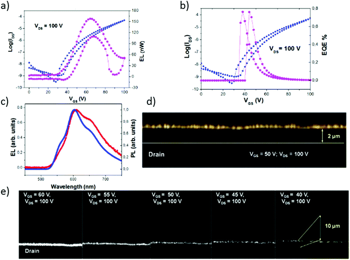
In this regard, it is worth comparing the OLET behavior of FT4N with that of NT4N, as a molecule which includes a second TI moiety in replacement of the fluorinated alkyl chain. Both compounds exhibited a V-shaped saturation transfer curve (i.e. by sweeping the gate voltage at a fixed source–drain voltage in saturation mode) which is typical of the ambipolar FET behavior. However, their charge mobilities were found to be drastically different. In particular, NT4N showed an outstanding electron-to-hole mobility ratio of 78.57 and p- and n-type charge mobilities respectively of 7 × 10⁻³ cm2 V−1 s−1 and 0.55 cm2 V−1 s−1 (Table 3).
As a result, an intense electroluminescence emission was observed from NT4N-based devices (Fig. 16), with an optical power up to 180 nW, that is more than three times higher than that emitted by FT4N (50 nW, Fig. 16d). The similarity of the electroluminescence spectrum of the NT4N-based OLET with the photoluminescence of a film of NT4N confirmed that the OLET emission originated from NT4N (Fig. 16c). As shown in Fig. 16a, the saturation transfer curve at VDS = 100 V of NT4N-based OLETs reported the electroluminescence signal peaked at about VGS ≈ ½ VDS, thus corresponding to the maximum hole–electron balance. In particular, at 50 V, which is a bias at which the emission intensity is still significant, the external quantum efficiency was found to be maximized (about 0.2%) (Fig. 16b). The pronounced ambipolarity shown by NT4N also enabled a fine tuning of the emission stripe position along the channel length of the OLET. Moreover, as shown in Fig. 16e, the emission zone could be spatially shifted by tuning the gate voltage. Despite the emissive stripe remaining in the proximity of the drain electrode due to the slight unbalance between charge mobilities, it was still well separated from the drain edge, thus preventing exciton quenching by the metal electrode or optical coupling effects of the emitted light with the metal electrodes.
As already introduced in section 2, tentative improvements of the OLET performance of NT4N were carried out by designing new compounds with modified inner-cores, such as NTzN and NThTN and NTMeN. Nevertheless, devices with mostly unipolar and non-emissive features were obtained in the case of NTzN and NThTn, while a transistor with good ambipolarity but drastically low p- and n-type mobilities was obtained from NTMeN (Table 3).
As a result, slight modifications were introduced in NT4N to further exploit all the advantages of that molecular structure. Despite hexyl or octyl functionalizations leading to NT4N-based OLETs emitting light 3 times more intense, the best ambipolar characteristics were still found from the use of the benchmark C4-NT4N (which is commonly named as NT4N). Having good ambipolar characteristics indeed allows the effective spatial tuning of the light stripe in OLETs.
The results discussed here also highlight the crucial role that molecular packing plays in the optoelectronic properties of oligothiophene derivatives. Indeed, a mix of phase A and phase B polymorphs with poor optoelectronic properties would be expected from the solution-processed deposition of Cx-NT4N including an even number of alkyl side chains, such as C4-NT4N, C6-NT4N and C8-NT4N. However, the intentional use of thermal sublimation as film-forming technique generates exclusively the polymorphic phase B, which is the only solid-state organization that guarantees the functionalities reported for NT4N-based OLETs.
In conclusion, the remarkable electroluminescence characteristics in conjunction with the best charge balance shown by C4-NT4N with respect to the other compounds identifies NT4N as the ideal candidate to further develop the OLET technology.
Despite the comparative analysis of the OLET emission intensities done throughout this section in terms of optical power, the standard evaluation of the emission intensity from solid-state devices is the measurement of the brightness. As a comparative value for the readers, the brightness reported from C6-NT4N based OLETs was about 20 cd m−2.70
NT4N-based OLET as a device platform for photonic application
OLETs represent a class of devices endowed with properties which are particularly suitable for real-settings applications in photonics. Combining electrical amplification with an efficient emission of light represents a direct route to develop functional pixels for displays at reduced costs and complexity. Furthermore, the possibility to move the light stripe in the horizontal plane of the device and to select the region where the exciton recombination occurs is of great interest also for sensing.86As shown in the previous sections, the use of semiconducting materials such as the class of NT4N derivatives offers also the benefit of obtaining devices with versatile optoelectronic characteristics.
All these features included in such a simple device in-plane geometry pave the way towards the engineering of OLETs to realize highly integrated organic optoelectronic devices with multiple novel functionalities.
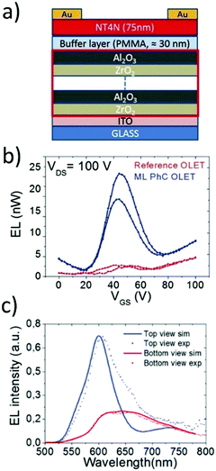
To this end, Natali et al. integrated a transparent multilayer photonic crystal (ML-PhC) as an optoelectronic gate dielectric to both modulate the light emission output and improve the electrical performance of NT4N-based OLETs.87 The ML-PhC consisted of a stack of nine alternating high-density layers of ZrO2 and Al2O3, and a 30 nm thick buffer layer of PMMA (Fig. 17a). The latter polymeric layer provided the surface for ensuring the molecular packing of NT4N with emissive and ambipolar field-effect behaviors.
The comparison with standard OLETs showed a 25-fold increased ambipolar source–drain current and, consequently, the optical power resulted in a ten-fold increase (Fig. 17b). The optoelectronic improvements were associated with the higher capacitance of the multilayered dielectric stack, that allowed the (i) decrease of both hole and electron gate thresholds, respectively of 13% and 46%, and (ii) increase in the EQE by a factor 3.
By changing the overall thickness of the dielectric structures, the authors prepared two different sets of integrated multilayered stacks with the aim of tuning the photonic bandgap of the photonic crystal and modulating the spatial distribution of the emitted photons. In particular, a dielectric structure, called ML-PhC λ1, was intentionally designed to locate the maximum of the NT4N EL spectrum in correspondence with the minimum of the ML-PhC transmittance spectrum. The dielectric stack was effectively demonstrated to work as a planar distributed Bragg reflector system, and an almost four-fold increase in the EL intensity was observed along the optical axis in the top view direction (Fig. 17c). In addition, an angular emission profile broader than the typical Lambertian one was recorded from the bottom side of the device.
Despite the great potential of ambipolar OLETs for real-setting applications, this type of device platform provides also the opportunity to investigate a plethora of different phenomena in a single nanometric layer such as hole and electron injection, field-effect conduction, charge recombination, light generation, and light extraction. By exploiting the in-plane geometry (thus avoiding possible disturbing metal electrodes) of transistors and the possibility of most organics to be photoexcited, the organic active layer in OLETs is accessible by optical scanning probe techniques for the investigation of the major photophysical and charge-correlated processes under device working-conditions.
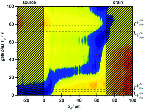
In this context, the ambipolar emissive features of NT4N-based OLETs were exploited by Koopman et al. to develop a unique approach for the determination of the contact resistance and the channel resistance in a single device.88 The new method involved the local observation of the charge density distribution within the transistor channel. In particular, photoluminescence electro-modulation microscopy was used to optically induce the formation of excitons and then to map their quenching due to the proximity of charges flowing in the organic semiconducting layer during device operation. The spatial localization of the ambipolar recombination region was evidenced by the enhanced fluorescence given by the additional electroluminescence from NT4N (blue region in Fig. 18).
The ambipolar regime was found to start at VGS around 10 V (in saturation regime of VDS = 100 V) and showed its maximum at VGS around 30 V. These values were crucial to understand the difference with respect to threshold voltages extracted from electrical characterization.
While values extrapolated from the typical electrical curves contained contribution from both contacts and channel resistances, threshold voltages extrapolated by this new approach contained only the voltage drop due to the contact resistance. The authors demonstrated that the contact resistance for the injection of electrons contributed only for the 6% of the total threshold voltage obtained electrically. The reported findings highlighted the possibility (i) to study how specific interfaces act during device operation and (ii) to identify the device-dependent and material-dependent issues that affect the electrical performance of devices. More importantly, authors showed that functional interfaces are way more complex than an energy mismatch between the metal Fermi level and the transport electronic levels of the semiconductor.
In this context, the same NT4N-based device was recently used to provide further insight into the complex correlation between the nature of the charge-injecting contacts and the electrical characteristics of devices.89 The authors showed how the presence of thienyl sulfur atoms in NT4N determined the formation of chemical interactions with gold electrodes, with the consequent formation of small gold nanoclusters during the first stages of contact formation. Multiple analyses repeated at different stages of device fabrication, including also synchrotron X-ray spectroscopy on devices in operando, showed that the electrical performance was the result of the interplay between (i) the chemical composition of metal electrodes and the OSC, (ii) the type of physicochemical interactions at the metal/OSC interface, (iii) the interfacial morphology and (iv) the organization of the metal clusters at the OSC interface.
We here provided some examples of the great potential offered by the implementation of TI-ended oligothiophene derivatives in the OLET device platform. The combination of ambipolar field-effect conduction, electroluminescence ability and simple tunability of the optoelectronic characteristics, endorse NT4N as a class of molecules suitable for fundamental investigations and technological development of multifunctional devices.
5. Conclusions
OLETs require the active materials to possess both high in-plane carrier mobility and high luminescence quantum yields to realize potential applications in active matrix full color displays, integrated photonic circuitry, sensing and possibly the long-searched electrically driven organic laser.However, OSCs (in particular small molecules) presenting high carrier mobility typically suffer from luminescence quenching in the solid state.
This simplistic thumb-rule has generally promoted the use of polymers as suitable organic conjugated semiconductors to be used in single-layer single-material ambipolar OLETs given their remarkable emissive properties in the solid state.
Significant effort must be put by the scientific community to synthesize and/or process active materials capable of balancing both high flowing charge-density and efficient rate of formation of emissive excitons.
In this scenario, this present study aimed at highlighting thienoimide-ended oligothiophenes as a new versatile family of multifunctional conjugated organic compounds which can be considered an ideal test-bed for investigating the relationships between the molecular structure, packing modalities, charge mobility and light emission in thin-films. As we have reported, the insertion of the TI moieties in the oligothiophene backbone proved to allow tuning of not only the optoelectronic properties of the semiconductors, thus passing from unipolar and non-electroluminescent molecules to ambipolar and electroluminescent ones, but also the material processability and self-assembly in nanostructured systems.
The peculiar packing mode of TI-ended oligothiophenes, that typically organize in the slipped π–π stacking packing mode differently from most oligothiophenes, is related to planarity, symmetry and alkyl-based end-substitutions in the molecular structure of these compounds. As a remarkable example in the state of the art of ambipolar organic conjugated molecules, the NT4N molecule shows an outstanding electron-to-hole mobility ratio of 78.57 and p- and n-type charge mobilities respectively of 7 × 10⁻³ cm2 V−1 s−1 and 0.55 cm2 V−1 s−1 differently from the unsymmetrical fluorinated counterpart.
The versatile chemical tuning of the molecular structure of TI-ended oligothiophenes (by both acting on the inner core and the terminations of the molecules) and the fine use of a confined environment during the crystallization process or of the suitable solution-processed or sublimation deposition techniques are the major tools for controlling the packing of molecules and their intermolecular interactions in the solid state. In this study, we clearly highlight that the analytical investigation of the correlation between polymorphism and optoelectronic performance in nanostructured systems implementing TI-ended oligothiophenes is the driver for designing and realizing multifunctional devices, such as real-time temperature integrators for color-dependent sensing and light-emitting transistors for switchable lighting.
By considering the field-effect transistor as a benchmark device platform and the extended family of TI-ended oligothiophenes as a case study in organic electronics, this study has assessed the quantification of optoelectronic figures of merit (such as charge mobility, gate threshold voltage, and emitted optical power) in OLETs by systematically varying the molecular structures and post-synthesis deposition approaches of the TI derivatives implemented as active material in OLETs.
The field of view has been further broadened in the study by including the report of the use of the NT4N-based OLETs as both scientific and technological viable solutions for optimizing the optoelectronic and photonic performance and envisaging the real-setting applications in OLETs.
The integration of a transparent multilayer photonic crystal as a dielectric stack in the architecture of a single-layer ambipolar OLET based on NT4N allows the realization of an innovative photonic device capable of probing and managing the direct optical coupling between electrically formed excitons and the planar photonic component in an electrode-free geometry.
Moreover, the direct access to the active channel and the remarkable ambipolar charge balance in transparent NT4N-based OLETs enable the use of these devices for optical imaging of the recombination zone location by means of an electro-optical scanning probe technique. Consequently, we expect that the same experimental methodology and test bench devices might be used to probe independently how the different functional interfaces in an organic transistor (such as the electrode/organic-semiconductor and the organic-semiconductor/dielectric) affect the charge-carrier injection, transport and recombination properties within the same single device, and in principle decouple the device-dependent and material-dependent issues that affect the electrical performance in organic field-effect transistors.
If we critically overview all the results reported here, it is evident that enormous effort is still needed for understanding the correlation between the compound molecular structure, the solid-state thin film arrangement and the functional properties as a function of thin-film process parameters. We believe that the development of multiscale computational methods could represent the key to boost the quantum and power efficiency of ambipolar OLETs. Despite the great progress that has been progressively achieved to estimate the optoelectronic characteristics of isolated molecules or small aggregated systems, this know-how must be evolved to include the entire device fabrication. As highlighted in this Perspective, the solid-state organization has a profound influence on the device characteristics. Each deposition technique specifically drives the thin-film formation and controls polymorphism. A comprehensive and predictive view of the entire process of device fabrication, from the synthesis of the single material to its implementation in the device to the design of functional interfaces, would open the way for a faster selection of materials and processing methods and dedicated developments for selected purposes.
In this regard, the strategy at the basis of the synthesis of TI-ended oligothiophene compounds contributes to the definition of a throughout multidisciplinary approach combining multiple material-processing techniques with structural, morphological, photophysical and optoelectronic systematic characterization of the nanostructured systems in order to achieve high-performing active materials for single-material single-layer OLETs.
Obtaining light-emission from an electrical switching and amplifying device is the major strength of the OLET platform. However, pursuing a dual functionality in a single architecture is also the major challenge of this technology that has still to be demonstrated in suitable application-driven paradigm in organic optoelectronics. In the near future, the major driver in the progress towards real-setting applications of OLET technology is the achievement of standards of performance in relation to high internal quantum efficiency values, outperforming the device outcoupling efficiency (allowing for a significant light fraction to be extracted outside the device) and lowering of the device operating voltages in order to minimize the device energy footprint.
We believe that the TI-ended oligothiophene family is a remarkable example of the introduction of new paradigms in designing organic semiconductors and engineering organic field-effect thin-film devices, which in turn may play a key-role in the demonstration of real-setting applications in electronics and photonics for organic compounds.
Conflicts of interest
There are no conflicts to declare.Acknowledgements
This work received funding from the European Union's Horizon 2020 Research and Innovation program under grant agreement no. 780839 (MOLOKO project). We kindly acknowledge the financial support from Programma Operativo POR-FESR 2014–2020 of Regione Emilia Romagna, Azione 1.2.2, through the project FORTRESS “Flexible, large-area patches for real-time detection of ionizing radiation”, CUP I38D18000150009 – PG/2018/629121.References
- J. Y. Oh, S. Rondeau-Gagné, Y.-C. Chiu, A. Chortos, F. Lissel, G.-J. N. Wang, B. C. Schroeder, T. Kurosawa, J. Lopez, T. Katsumata, J. Xu, C. Zhu, X. Gu, W.-G. Bae, Y. Kim, L. Jin, J. W. Chung, J. B.-H. Tok and Z. Bao, Nature, 2016, 539, 411–415 CrossRef CAS.
- O. Ostroverkhova, Chem. Rev., 2016, 116, 13279–13412 CrossRef CAS.
- P. W. M. Blom, Adv. Mater. Technol., 2020, 5, 2000144 CrossRef CAS.
- R.-P. Xu, Y.-Q. Li and J.-X. Tang, J. Mater. Chem. C, 2016, 4, 9116–9142 RSC.
- M. A. Baldo, D. F. O’Brien, Y. You, A. Shoustikov, S. Sibley, M. E. Thompson and S. R. Forrest, Nature, 1998, 395, 151–154 CrossRef CAS.
- J. H. Burroughes, D. D. C. Bradley, A. R. Brown, R. N. Marks, K. Mackay, R. H. Friend, P. L. Burns and A. B. Holmes, Nature, 1990, 347, 539–541 CrossRef CAS.
- H. F. Wittmann, J. Grüner, R. H. Friend, G. W. C. Spencer, S. C. Moratti and A. B. Holmes, Adv. Mater., 1995, 7, 541–544 CrossRef CAS.
- J. Feng, Y.-F. Liu, Y.-G. Bi and H.-B. Sun, Laser Photonics Rev., 2017, 11, 1600145 CrossRef.
- M. Muccini and S. Toffanin, Organic Light-Emitting Transistors: Towards the Next Generation Display Technology, Wiley, 2016 Search PubMed.
- M. Muccini, W. Koopman and S. Toffanin, Laser Photonics Rev., 2012, 6, 258–275 CrossRef CAS.
- S. Toffanin, R. Capelli, W. Koopman, G. Generali, S. Cavallini, A. Stefani, D. Saguatti, G. Ruani and M. Muccini, Laser Photonics Rev., 2013, 7, 1011–1019 CrossRef CAS.
- R. Capelli, S. Toffanin, G. Generali, H. Usta, A. Facchetti and M. Muccini, Nat. Mater., 2010, 9, 496–503 CrossRef CAS.
- M. Muccini, Nat. Mater., 2006, 5, 605–613 CrossRef CAS.
- M. U. Chaudhry, K. Muhieddine, R. Wawrzinek, J. Sobus, K. Tandy, S. Lo and E. B. Namdas, Adv. Funct. Mater., 2020, 30, 1905282 CrossRef CAS.
- J. Zaumseil, Adv. Funct. Mater., 2020, 30, 1905269 CrossRef CAS.
- T. Sakanoue, M. Yahiro, C. Adachi, J. H. Burroughes, Y. Oku, N. Shimoji, T. Takahashi and A. Toshimitsu, Appl. Phys. Lett., 2008, 92, 053505 CrossRef.
- M. Ullah, R. Wawrzinek, R. C. R. Nagiri, S.-C. Lo and E. B. Namdas, Adv. Opt. Mater., 2017, 5, 1600973 CrossRef.
- F. Dinelli, R. Capelli, M. A. Loi, M. Murgia, M. Muccini, A. Facchetti and T. J. Marks, Adv. Mater., 2006, 18, 1416–1420 CrossRef CAS.
- M. Zambianchi, E. Benvenuti, C. Bettini, C. Zanardi, R. Seeber, D. Gentili, M. Cavallini, M. Muccini, V. Biondo, C. Soldano, G. Generali, S. Toffanin and M. Melucci, J. Mater. Chem. C, 2016, 4, 9411–9417 RSC.
- M. Prosa, E. Benvenuti, M. Pasini, U. Giovanella, M. Bolognesi, L. Meazza, F. Galeotti, M. Muccini and S. Toffanin, ACS Appl. Mater. Interfaces, 2018, 10, 25580–25588 CrossRef CAS.
- Z. Xu, S.-H. Li, L. Ma, G. Li and Y. Yang, Appl. Phys. Lett., 2014, 4 Search PubMed.
- M. Ullah, R. Wawrzinek, F. Maasoumi, S.-C. Lo and E. B. Namdas, Adv. Opt. Mater., 2016, 4, 1022–1026 CrossRef CAS.
- B. B. Y. Hsu, C. Duan, E. B. Namdas, A. Gutacker, J. D. Yuen, F. Huang, Y. Cao, G. C. Bazan, I. D. W. Samuel and A. J. Heeger, Adv. Mater., 2012, 24, 1171–1175 CrossRef CAS.
- J.-H. Lee, T.-H. Ke, J. Genoe, P. Heremans and C. Rolin, Adv. Electron. Mater., 2019, 5, 1800437 CrossRef.
- S. D. Kang and G. J. Snyder, Nat. Mater., 2017, 16, 252–257 CrossRef.
- C. Wang, H. Dong, W. Hu, Y. Liu and D. Zhu, Chem. Rev., 2012, 112, 2208–2267 CrossRef CAS.
- K. Zhou, H. Dong, H. Zhang and W. Hu, Phys. Chem. Chem. Phys., 2014, 16, 22448–22457 RSC.
- J. T. E. Quinn, J. Zhu, X. Li, J. Wang and Y. Li, J. Mater. Chem. C, 2017, 5, 8654–8681 RSC.
- J.-L. Brédas, D. Beljonne, V. Coropceanu and J. Cornil, Chem. Rev., 2004, 104, 4971–5004 CrossRef.
- P. Mei, M. Murgia, C. Taliani, E. Lunedei and M. Muccini, J. Appl. Phys., 2000, 88, 5158–5165 CrossRef CAS.
- D. Gedefaw, M. Prosa, M. Bolognesi, M. Seri and M. R. Andersson, Adv. Energy Mater., 2017, 7, 1700575 CrossRef.
- D. Gedefaw, M. Tessarolo, M. Bolognesi, M. Prosa, R. Kroon, W. Zhuang, P. Henriksson, K. Bini, E. Wang, M. Muccini, M. Seri and M. R. Andersson, Beilstein J. Org. Chem., 2016, 12, 1629–1637 CrossRef CAS.
- Z. Li, X. Xu, W. Zhang, Z. Genene, W. Mammo, A. Yartsev, M. R. Andersson, R. A. J. Janssen and E. Wang, J. Mater. Chem. A, 2017, 5, 11693–11700 RSC.
- M. Seri, D. Gedefaw, M. Prosa, M. Tessarolo, M. Bolognesi, M. Muccini and M. R. Andersson, J. Polym. Sci., Part A: Polym. Chem., 2017, 55, 234–242 CrossRef CAS.
- X. Chen, G. Zhang, H. Luo, Y. Li, Z. Liu and D. Zhang, J. Mater. Chem. C, 2014, 2, 2869–2876 RSC.
- S. Bonetti, M. Prosa, A. Pistone, L. Favaretto, A. Sagnella, I. Grisin, M. Zambianchi, S. Karges, A. Lorenzoni, T. Posati, R. Zamboni, N. Camaioni, F. Mercuri, M. Muccini, M. Melucci and V. Benfenati, J. Mater. Chem. B, 2016, 4, 2921–2932 RSC.
- A. Riaño, P. M. Burrezo, M. J. Mancheño, A. Timalsina, J. Smith, A. Facchetti, T. J. Marks, J. T. L. Navarrete, J. L. Segura, J. Casado and R. P. Ortiz, J. Mater. Chem. C, 2014, 2, 6376–6386 RSC.
- C. L. Donley, J. Zaumseil, J. W. Andreasen, M. M. Nielsen, H. Sirringhaus, R. H. Friend and J.-S. Kim, J. Am. Chem. Soc., 2005, 127, 12890–12899 CrossRef CAS.
- J.-S. Kim, P. K. H. Ho, C. E. Murphy and R. H. Friend, Macromolecules, 2004, 37, 2861–2871 CrossRef CAS.
- X. Cheng, Y.-Y. Noh, J. Wang, M. Tello, J. Frisch, R.-P. Blum, A. Vollmer, J. P. Rabe, N. Koch and H. Sirringhaus, Adv. Funct. Mater., 2009, 19, 2407–2415 CrossRef CAS.
- J. Zaumseil, R. J. Kline and H. Sirringhaus, Appl. Phys. Lett., 2008, 92, 073304 CrossRef.
- M. Melucci, M. Durso, C. Bettini, M. Gazzano, L. Maini, S. Toffanin, S. Cavallini, M. Cavallini, D. Gentili, V. Biondo, G. Generali, F. Gallino, R. Capelli and M. Muccini, J. Mater. Chem. C, 2014, 2, 3448 RSC.
- F. Garnier, R. Hajlaoui, A. El Kassmi, G. Horowitz, L. Laigre, W. Porzio, M. Armanini and F. Provasoli, Chem. Mater., 1998, 10, 3334–3339 CrossRef CAS.
- H. E. Katz, A. J. Lovinger and J. G. Laquindanum, Chem. Mater., 1998, 10, 457–459 CrossRef CAS.
- R. Capelli, F. Dinelli, S. Toffanin, F. Todescato, M. Murgia, M. Muccini, A. Facchetti and T. J. Marks, J. Phys. Chem. C, 2008, 112, 12993–12999 CrossRef CAS.
- M. Durso, D. Gentili, C. Bettini, A. Zanelli, M. Cavallini, F. De Angelis, M. Grazia Lobello, V. Biondo, M. Muccini, R. Capelli and M. Melucci, Chem. Commun., 2013, 49, 4298–4300 RSC.
- D. Fichou, J. Mater. Chem., 2000, 10, 571–588 RSC.
- E. Benvenuti, D. Gentili, F. Chiarella, A. Portone, M. Barra, M. Cecchini, C. Cappuccino, M. Zambianchi, S. G. Lopez, T. Salzillo, E. Venuti, A. Cassinese, D. Pisignano, L. Persano, M. Cavallini, L. Maini, M. Melucci, M. Muccini and S. Toffanin, J. Mater. Chem. C, 2018, 6, 5601–5608 RSC.
- I. F. Perepichka and D. F. Perepichka, Handbook of Thiophene-Based Materials: Applications in Organic Electronics and Photonics, John Wiley & Sons, 2009 Search PubMed.
- T. Benincori, M. Capaccio, F. De Angelis, L. Falciola, M. Muccini, P. Mussini, A. Ponti, S. Toffanin, P. Traldi and F. Sannicolò, Chem. – Eur. J., 2008, 14, 459–471 CrossRef CAS.
- G. Barbarella, M. Melucci and G. Sotgiu, Adv. Mater., 2005, 17, 1581–1593 CrossRef CAS.
- M. Melucci, G. Barbarella, M. Zambianchi, P. Di Pietro and A. Bongini, J. Org. Chem., 2004, 69, 4821–4828 CrossRef CAS.
- S. Gronowitz, Thiophene and Its Derivatives, Part 1–5, John Wiley & Sons, 1985 Search PubMed.
- S. Gronowitz, Thiophenes, Elsevier, 2004 Search PubMed.
- A. Yassar, F. Demanze, A. Jaafari, M. E. Idrissi and C. Coupry, Adv. Funct. Mater., 2002, 12, 699–708 CrossRef CAS.
- A. Facchetti, M.-H. Yoon, C. L. Stern, H. E. Katz and T. J. Marks, Angew. Chem., 2003, 115, 4030–4033 CrossRef.
- A. Facchetti, M.-H. Yoon, C. L. Stern, G. R. Hutchison, M. A. Ratner and T. J. Marks, J. Am. Chem. Soc., 2004, 126, 13480–13501 CrossRef CAS.
- H. Usta, A. Facchetti and T. J. Marks, Acc. Chem. Res., 2011, 44, 501–510 CrossRef CAS.
- S. Trasatti, Pure Appl. Chem., 1986, 58, 955–966 CAS.
- G. Zotti, G. Schiavon, A. Berlin and G. Pagani, Chem. Mater., 1993, 5, 620–624 CrossRef CAS.
- G. Zotti, G. Schiavon, A. Berlin and G. Pagani, Chem. Mater., 1993, 5, 430–436 CrossRef CAS.
- G. Zotti, G. Schiavon, A. Berlin and G. Pagani, Synth. Met., 1993, 61, 81–87 CrossRef CAS.
- M. Melucci, M. Zambianchi, L. Favaretto, M. Gazzano, A. Zanelli, M. Monari, R. Capelli, S. Troisi, S. Toffanin and M. Muccini, Chem. Commun., 2011, 47, 11840 RSC.
- J. Heinze, B. A. Frontana-Uribe and S. Ludwigs, Chem. Rev., 2010, 110, 4724–4771 CrossRef CAS.
- A. Mishra, C.-Q. Ma and P. Bäuerle, Chem. Rev., 2009, 109, 1141–1276 CrossRef CAS.
- L. Pauling, The Nature of the Chemical Bond, Cornell University, Ithaca, NY, 1945 Search PubMed.
- M. Melucci, L. Favaretto, M. Zambianchi, M. Durso, M. Gazzano, A. Zanelli, M. Monari, M. G. Lobello, F. De Angelis, V. Biondo, G. Generali, S. Troisi, W. Koopman, S. Toffanin, R. Capelli and M. Muccini, Chem. Mater., 2013, 25, 668–676 CrossRef CAS.
- M. Zambianchi, L. Favaretto, M. Durso, C. Bettini, A. Zanelli, I. Manet, M. Gazzano, L. Maini, D. Gentili, S. Toffanin, F. Gallino, M. Muccini, M. Cavallini and M. Melucci, J. Mater. Chem. C, 2015, 3, 121–131 RSC.
- S. Oku, K. Takamiya, D. Adachi, S. Ishikawa, S. Nagamatsu, W. Takashima, S. Hayase and K. Kaneto, Chem. Lett., 2010, 39, 1315–1316 CrossRef CAS.
- M. Melucci, M. Durso, C. Bettini, M. Gazzano, L. Maini, S. Toffanin, S. Cavallini, M. Cavallini, D. Gentili, V. Biondo, G. Generali, F. Gallino, R. Capelli and M. Muccini, J. Mater. Chem. C, 2014, 2, 3448–3456 RSC.
- L. Maini, F. Gallino, M. Zambianchi, M. Durso, M. Gazzano, K. Rubini, D. Gentili, I. Manet, M. Muccini, S. Toffanin, M. Cavallini and M. Melucci, Chem. Commun., 2015, 51, 2033–2035 RSC.
- C. Cappuccino, P. P. Mazzeo, T. Salzillo, E. Venuti, A. Giunchi, R. G. D. Valle, A. Brillante, C. Bettini, M. Melucci and L. Maini, Phys. Chem. Chem. Phys., 2018, 20, 3630–3636 RSC.
- C. Cappuccino, S. Canola, G. Montanari, S. G. Lopez, S. Toffanin, M. Melucci, F. Negri and L. Maini, Cryst. Growth Des., 2019, 19, 2594–2603 CrossRef CAS.
- D. Gentili, M. Durso, C. Bettini, I. Manet, M. Gazzano, R. Capelli, M. Muccini, M. Melucci and M. Cavallini, Sci. Rep., 2013, 3, 2581 CrossRef.
- D. Gentili, I. Manet, F. Liscio, M. Barbalinardo, S. Milita, C. Bettini, L. Favaretto, M. Melucci, A. Fraleoni-Morgera and M. Cavallini, Chem. Commun., 2020, 56, 1689–1692 RSC.
- D. Gentili, F. Liscio, L. Mariucci, L. Beverina, M. Melucci, S. Toffanin, S. Milita and M. Cavallini, Adv. Funct. Mater., 2016, 26, 2387–2393 CrossRef CAS.
- M. U. Chaudhry, N. Wang, K. Tetzner, A. Seitkhan, Y. Miao, Y. Sun, M. C. Petty, T. D. Anthopoulos, J. Wang and D. D. C. Bradley, Adv. Electron. Mater., 2019, 5, 1800985 CrossRef.
- A. Hepp, H. Heil, W. Weise, M. Ahles, R. Schmechel and H. von Seggern, Phys. Rev. Lett., 2003, 91, 157406 CrossRef.
- H. Nakanotani, M. Saito, H. Nakamura and C. Adachi, Appl. Phys. Lett., 2009, 95, 103307 CrossRef.
- K. Sawabe, T. Takenobu, S. Z. Bisri, T. Yamao, S. Hotta and Y. Iwasa, Appl. Phys. Lett., 2010, 97, 043307 CrossRef.
- S. Z. Bisri, T. Takenobu, Y. Yomogida, H. Shimotani, T. Yamao, S. Hotta and Y. Iwasa, Adv. Funct. Mater., 2009, 19, 1728–1735 CrossRef CAS.
- T. Takahashi, T. Takenobu, J. Takeya and Y. Iwasa, Adv. Funct. Mater., 2007, 17, 1623–1628 CrossRef CAS.
- R. Ding, M. An, J. Feng and H. Sun, Laser Photonics Rev., 2019, 13, 1900009 CrossRef CAS.
- S. Hotta, T. Yamao, S. Z. Bisri, T. Takenobu and Y. Iwasa, J. Mater. Chem. C, 2014, 2, 965–980 RSC.
- M. Durso, C. Bettini, A. Zanelli, M. Gazzano, M. G. Lobello, F. De Angelis, V. Biondo, D. Gentili, R. Capelli, M. Cavallini, S. Toffanin, M. Muccini and M. Melucci, Org. Electron., 2013, 14, 3089–3097 CrossRef CAS.
- M. Prosa, M. Bolognesi, L. Fornasari, G. Grasso, L. Lopez-Sanchez, F. Marabelli and S. Toffanin, J. Nanomater., 2020, 10, 480 CrossRef CAS.
- M. Natali, S. D. Quiroga, L. Passoni, L. Criante, E. Benvenuti, G. Bolognini, L. Favaretto, M. Melucci, M. Muccini, F. Scotognella, F. Di Fonzo and S. Toffanin, Adv. Funct. Mater., 2017, 27, 1605164 CrossRef.
- W. W. A. Koopman, M. Natali, C. Bettini, M. Melucci, M. Muccini and S. Toffanin, ACS Appl. Mater. Interfaces, 2018, 10, 35411–35419 CrossRef CAS.
- M. Natali, M. Prosa, A. Longo, M. Brucale, F. Mercuri, M. Buonomo, N. Lago, E. Benvenuti, F. Prescimone, C. Bettini, A. Cester, M. Melucci, M. Muccini and S. Toffanin, ACS Appl. Mater. Interfaces, 2020, 12, 30616–30626 CrossRef CAS.
Footnote |
| † M. P. and S. M. contributed equally to this work. |
| This journal is © The Royal Society of Chemistry 2020 |

