 Open Access Article
Preparation of SnO2 nanotubes via a template-free electrospinning process
Takahiro Suzukiab,
Jing Chenga,
Li Qiaoc,
Yan Xing a,
Meng Fei Zhanga,
Hiroki Nishijimad,
Tetsuji Yanob and
Wei Pan
 *a
*a
aState Key Laboratory of New Ceramic and Fine Processing, School of Materials Science and Engineering, Tsinghua University, Beijing 100084, P. R. China. E-mail: panw@mail.tsinghua.edu.cn
bDepartment of Materials Science and Engineering, Tokyo Institute of Technology, 2-12-1 Ookayama, Meguro, Tokyo 152-8550, Japan
cDepartment of Basic Research, Qinghai University, Xining 810016, P. R. China
dFunctional Material Department, Inorganic Material Engineering Division, Toyota Motor Corporation, Toyota, Aichi 471-8572, Japan
First published on 10th June 2020
Abstract
A facile and environmentally friendly template-free method is developed for the fabrication of SnO2 nanotubes via electrospinning and precisely controlled heat treatment method. It is revealed that the as-spun solid SnO2 precursor fibers gradually transformed into hollow-structured nanotubes when the temperature was controlled precisely from 200 °C to 600 °C. It was confirmed, that this remarkable structural evolution corporate the respective thermal decomposition of polyvinyl butyral (PVB) at the surface and inside of the fibers. The formation mechanism of the nanotubes has been clarified by systematically investigating the morphology, phase structure, chemical state, and decomposition of the organic compounds during the heat treatment. The as-prepared SnO2 nanotubes exhibit a high specific surface area of 32.91 m2 g−1 and a porous structure with pore sizes of 2 nm and 10–25 nm. The SnO2 nanotubes were assembled as a photosensor, which demonstrates a fast response upon UV light illumination at 254 nm. From this discovery, it is expected that a new method for fabricating nanotubes will be established and the development of materials with a higher functionality will be promoted.
Introduction
As a kind of n-type semiconductor oxide, tin oxide (SnO2) having a bandgap of 3.6 eV has been extensively studied in the field of the solar cells, gas sensors, and lithium-ion batteries.1,2 Nowadays, numerous approaches have been investigated to improve its performances, including preparing nanostructured SnO2 with increased surface area to volume ratio.3–5 Recently, one-dimensional SnO2 nanostructures having high surface to volume ratios, such as nanofibers, nanoribbons, nanowires, nanobelts, and nanotubes, have attracted attention.Among various one-dimensional SnO2 nanostructures, the SnO2 nanotubes have attracted intense scientific interest due to their fantastic physical, mechanical, and optical properties. The nanotubes are mostly synthesized by methods such as anodic oxidation,6 chemical or physical deposition on sacrificial templates,7 and hydrothermal treatment.8
Although there are numerous approaches to obtain the nanotubes, the currently used methods have disadvantages such as not being environmentally friendly, complicated processes, and inefficient. Electrospinning is a simple and cost-effective method to fabricate one-dimensional organic materials and inorganic materials.9–11 Coaxial electrospinning is a mature method for the synthesis of nanotubes using a mineral oil as a core template material.12,13 By calcining the obtained two-layered nanofibers at a high temperature under air, the mineral oil of the core is removed, and nanotubes are obtained.10 However, removing the oil would cause environmental pollution.
Here, we have designed a template-free process to prepare SnO2 nanotubes by combining electrospinning and Ostwald ripening processes. Ostwald ripening is a classical physical phenomenon in crystal growth. This ripening process involves “the growth of larger crystals from the smaller ones that have a higher solubility than the larger ones.”14,15 It is based on the differences in sizes between the inner and outer crystallites in the precursor fibers to obtain the hollow structure. In the present study, SnO2 nanotubes were fabricated by electrospinning polyvinyl butyral (PVB)/Sn precursor composite nanofibers, followed by precisely controlled heat treatment. PVB is a non-toxic, odorless, environmentally-friendly polymer, which has excellent compatibility with inorganic materials and is widely used for the production of organic/inorganic hybrid composites. In the published articles there are several choices for the organic additives for the precursor solutions, such as PVP, DMF, EC, and DMC.1,16–21 Fabricated nanotubes also have excellent recyclability, transparency, toughness, flexibility, and excellent adhesion.22–25 In our study, we selected PVB and ethanol as solvents and no other additives were involved. The steps and mechanisms for the formation of the hollow-structured SnO2 nanotubes are investigated and discussed.
Experimental
Synthesis of SnO2 nanotube
SnO2 nanotubes were synthesized via a combination of sol–gel based electrospinning and subsequent heat treatment. Ethanol and polyvinyl butyral (PVB), were purchased from Sinopharm Chemical Reagent Co., Ltd. SnCl2·2H2O was purchased from Beijing Yili Fine Chemical Co., Ltd., and all the chemicals were of analytical reagent grade. The precursor solution was prepared by dissolving SnCl2·2H2O (0.3 g) in ethanol (8 g) and then mixed with PVB (0.6 g). The as-prepared precursor solution was delivered into a syringe with a stainless-steel needle. Precursor fibers were obtained via an electrospinning setup with a voltage of 9.25 kV applied on the needle tip and a collector ground aluminum foil with a distance of 15 cm between the needle and collector. The as-spun fibers were peeled off from the aluminium foil used as a collector and heat-treated in the air at 200 °C, 300 °C, 400 °C, 500 °C, 550 °C, 600 °C, 700 °C. The heating rate was maintained at 10 °C min−1.Characterization
The crystal structure of samples was investigated via X-ray diffraction (XRD, D8 Advance, Bruker, Germany) with Cu Kα radiation (0.15418 nm) operating at 40 kV. X-ray photoelectron spectroscopy (XPS, PHI-5300 ESCA, PerkinElmer, Boston, MA, USA) was performed to analyse the elemental and chemical states of the material. The morphology of the samples was studied via field emission scanning electron microscopy (FE-SEM, LEO-1530, Carl Zeiss, Germany). Moreover, the morphology and energy-dispersive X-ray spectroscopy (EDS) studies were performed on the samples using a transmission electron microscope (TEM, JEM-2100F, JEOL, Japan). Fourier transform infrared (FTIR) spectra were recorded using a spectrometer (BRUKER VERTEX37 70V, USA) in the frequency range of 500–4500 cm−1, with a resolution of 4 cm−1. Thermogravimetric analysis and Fourier transform IR spectroscopy were combined to analyse the thermogravimetric data in real-time to analyse the released volatile by-products (STA449F3 DSC TGA and Bruker Vertex70V). During testing, specimens were heated in an alumina crucible at a heating rate of 10 °C min−1, and the IR spectra were recorded with a spectral resolution of 4 cm−1. The specific surface area was determined by a single point Brunauer–Emmet–Teller (BET) method through nitrogen adsorption using the Quadrasorb SI-MP (Quantachrome Instruments USA). The specimen weight was about 0.1 g. UV photodetection measurements were performed by Keithley interactive test environment (Keithley 4200, Keithley Instruments, USA).Result and discussion
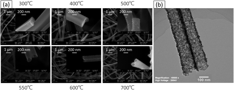
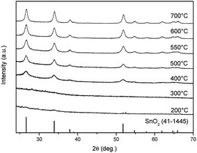
Fig. 1 demonstrates the morphologies of the precursor nanofibers after heat treatment at different temperatures. The surface of the nanofibers shows smooth and solid structures below 500 °C that translates into nanotubes as the temperature is elevated above 550 °C. From the TEM observation, the diameter of nanotubes is about 120 nm, and the thickness of the wall is about 10 nm when the nanotubes are annealed at 600 °C (Fig. 1). The crystal structures of the as-spun nanofibers and heat-treated samples were characterized via XRD and the data obtained are shown in Fig. 2. The diffraction peaks cannot be confirmed at 300 °C, which indicates the amorphous nature of PVB/Sn in the nanofibers. Moreover, it is confirmed from the peak intensities of the (1 1 0), (1 0 1) and (2 1 1) planes that the crystal growth of SnO2 starts at 400 °C, and it grows as the temperature increases. It is found that the diffraction peaks of the SnO2 crystal became sharper as the temperature of the heat treatment increased, which indicates the growth of the SnO2 crystals. From these diffraction peaks, it is shown that SnO2 is a tetragonal type (JCPDS 41-1445).Thermogravimetric analysis (TG) was carried out to investigate the mass change of the as-spun fibers during the heat treatment for understanding the mechanism of the formation of the nanotubes from a solid precursor nanofiber by heat treatment. The TG graph of PVB/Sn precursor nanofibers is shown in Fig. 3. From this graph, it is found that the as-spun fibers show two mass-loss stages during the heating cycle. Stage 1 occurs up to 230 °C; at this stage 51% weight loss is determined. Stage 2 is from 230 °C to 600 °C, and 30% weight loss is confirmed. The corresponding FESEM images of the samples taken at different temperatures are shown as insets in the TG result graph. It is seen that the surface of the sample is smooth even after stage 1, which is the initial weight loss stage. Then, the weight loss stage 2 occurs, a core fiber forms inside the tube, and the process finally led to the formation of a tubular structure as the inside fiber contracts and disappears.
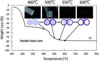 | ||
| Fig. 3 TG patterns of PVB/Sn precursor composite nanofibers with corresponding SEM images after 400 °C, 500 °C, 550 °C, and 600 °C heat treatments. | ||
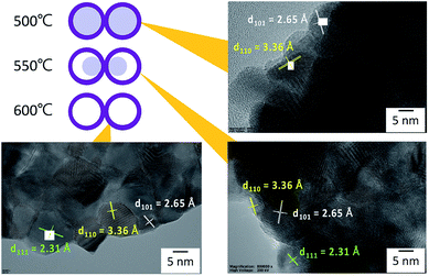
From the SEM observation, it is seen that the fiber transforms into a tube structure from 500 °C to 600 °C. The TEM and EDS linear scans were performed on samples heat-treated at different temperatures to investigate how the ions move during the process from the fiber to the tube. The high magnification TEM images of the surface at each temperature are shown in Fig. 4. It is found from the interplanar distance that the crystal present on the surface of the tube is SnO2 at all temperature ranges. Each of the interplanar distance of 3.36 Å, 2.65 Å and 2.31 Å are assigned to the (1 1 0), (1 0 1), and (1 1 1) planes, respectively.21 TEM images and EDS linear scan results of the 500 °C heat treatment sample are shown in Fig. 5. EDS linear scan of the 500 °C sample indicates that the concentration of the Sn and O ions in the outer shell is high. This result is believed to involve the volatilization of ethanol during electrospinning. It is known that the solubility of Sn ions in ethanol is higher than that of PVB. In electrospinning, the solution volatilizes during depositing on to the collector. While volatilizing, Sn ions with high solubility in ethanol are considered to be more easily carried to the surface compared to PVB.26 The surface of the sample is exposed to air that contains a high concentration of oxygen. PVB decomposes during annealing and Sn ions change to SnO2 with increasing temperature. On the contrary, carbon concentration is highly associated with the decomposed PVB residues inside the fibers. It is seen that the PVB residues are almost oxidized in the outer shell, but trace amounts of C could be observed inside.
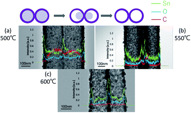 | ||
| Fig. 5 TEM images of 500 °C (a), 550 °C (b), and 600 °C (c) with the line profiles across the samples of the three specimens. | ||
The TEM image and the EDS linear scan results of the sample annealed at 550 °C are shown in Fig. 5(b). At this temperature, it is clear from the SEM results shown in Fig. 1 and 3 that the tube structure is formed in the fiber. From the results of the EDS linear scan, elements Sn and O show sharp peaks at the shell. Besides, C remains at the junction of the two tubes.
It is demonstrated from the SEM results that the tube shape is formed at 600 °C. The composition of the tube structure is pure SnO2 crystals, as seen from the XRD results. Fig. 5(c) shows that the C signal of the linear scan is very weak demonstrating that the carbon is almost removed after 600 °C annealing. Also, from the TEM image, it is seen that the structure of the nanotubes is porous. When the heat treatment temperature is changed from 500 °C to 600 °C, it is found that in the process of forming a tube, C is moved toward the outer shell with the internal fiber shrinkage.
According to the simulation results of Ravishankar et al.,27 when a shell on the surface is formed early in the bulk, it tends to finally result in a hollow structure. Moreover, there are numerous studies that use the Ostwald ripening mechanism to explain the formation of hollow structures.28–31 Referencing the literature, in the present research, the nanotube formation process may also be interpreted by the Ostwald ripening mechanism. In order to confirm the mechanism, a detailed analysis was performed via XPS, TG-FTIR, FTIR because the decomposition of PVB accompanying increase temperature was of much concern.
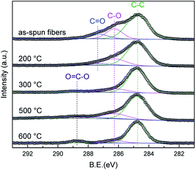
Fig. 6 shows the spectrum of the C 1s of the as-spun fibers and heat-treated samples at each temperature. Four peaks are confirmed in the as-spun fibers. The four peaks at 284.7, 286.3, 287.4, and 288.7 eV are assigned to the C–C, C–O, C![[double bond, length as m-dash]](https://www.rsc.org/images/entities/char_e001.gif) O, and O
O, and O![[double bond, length as m-dash]](https://www.rsc.org/images/entities/char_e001.gif) C–O bands, respectively.32,33 The C
C–O bands, respectively.32,33 The C![[double bond, length as m-dash]](https://www.rsc.org/images/entities/char_e001.gif) O band is a side substituent of the PVB structure, the peak intensity decreases from the as-spun to 200 °C, and disappears above 300 °C. It is believed that PVB on the surface is decomposed at 300 °C even though no significant change is observed in the spectra above 300 °C annealing. This XPS result supports the linear analysis results that PVB on the surface was already decomposed at 500 °C.
O band is a side substituent of the PVB structure, the peak intensity decreases from the as-spun to 200 °C, and disappears above 300 °C. It is believed that PVB on the surface is decomposed at 300 °C even though no significant change is observed in the spectra above 300 °C annealing. This XPS result supports the linear analysis results that PVB on the surface was already decomposed at 500 °C.
Rapid scanning Fourier transform infrared in situ spectroscopy was used to investigate the volatile products formed during the heat treatment process of the as-spun fibers. The results are demonstrated in Fig. 7. It is seen that as the temperature increases, changes are happening in two stages. The first stage starts around 200 °C, and a pattern with a complex peak is seen near 300 °C. It is well known that PVB decomposes into a plurality of volatile substances as the temperature increases. Among various volatile substances, the occurrence of butanal is known to be the most prominent.34 From this spectra, it is considered that the decomposition products substances volatilized are acetic acid, butanoic acid, butenal, butanol, and furan.35 The second stage starts from 300 °C and the peaks located between 2310 cm−1 and 2356 cm−1 are known to be the peaks of CO2.36,37 The analysis results are consistent with those obtained from XPS and TG.
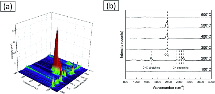 | ||
| Fig. 7 IR spectra of volatile byproducts from the decomposition of as-spun fibers. (a) IR spectra in whole temperature range. (b) IR spectra collected at various temperatures. | ||
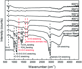
FTIR was used to investigate the residues of fibers during the heat treatment for the formation of SnO2 nanotubes. The results of the FTIR are shown in Fig. 8. The peak of 3200–3600 cm−1 is derived from the –OH stretching vibration.26,38,41,42 It is confirmed that the specific peak of PVB disappears at around 300 °C when the as-spun fibers were heated at 10 °C min−1. The peak seen at 660 cm−1 which is derived from the stretching mode of Sn–O begins to appear in the regional signals at around 400 °C.39 This result is consistent with the XRD analysis. The spectrum of the as-spun fibers is attributed to PVB. The peak at 2945 cm−1 is derived from the aliphatic CH stretching vibration. The peaks at 1431 cm−1 and 1377 cm−1 are derived from CH2 and CH3 bending mode, respectively.40 The peaks at 999 cm−1 and 1245 cm−1 are derived from the C–O–C stretching vibration of the acetate group. The peak at 1133 cm−1 is assumed to be from the C–O–C–O–C stretching vibrations of the butyral ring.41 These peaks almost disappeared at 300 °C. These results are consistent with TG-FTIR results, which showed that substances such as butanal were completely volatile as a result of the decomposition of the butyral group. As the temperature increases, the peak intensities of 1263 cm−1, 1614 cm−1, and 1705 cm−1 were maintained. These are attributed to the C–O–C stretching vibration, semicircle aromatic ring, and C![[double bond, length as m-dash]](https://www.rsc.org/images/entities/char_e001.gif) O stretching vibrations, respectively.42 During the process of PVB decomposition, it is known that the organic compounds of the cyclic structure and the crosslinked compounds are formed according to the free radical mechanism in a leaner oxygen environment. It is predicted that the decomposition of this cyclic structure and the crosslinked compounds reduced CO2, and this is considered as the stage 2 decomposition.42 The volatilized substances are supposed to have moved from the inside of fiber to the outside. It is predicted that accompanying this movement of the volatilized substances, small SnO2 crystals also moved to the outer shell and crystals grew on the outer shell. In other articles, using PVP for the precursor solution, it was observed that the PVP decomposition started at about 300 °C, and the movement of PVP residues and CO2 contributed to the formation of SnO2 nanotubes.16–21 In this study, the PVB precursor nanofibers started decomposing at 230 °C and during heating till 600 °C the fibers endured nealy 3 stage decomposition reactions to change into SnO2 nanotubes and the formation mechanism may be explained by the Ostwald ripening.
O stretching vibrations, respectively.42 During the process of PVB decomposition, it is known that the organic compounds of the cyclic structure and the crosslinked compounds are formed according to the free radical mechanism in a leaner oxygen environment. It is predicted that the decomposition of this cyclic structure and the crosslinked compounds reduced CO2, and this is considered as the stage 2 decomposition.42 The volatilized substances are supposed to have moved from the inside of fiber to the outside. It is predicted that accompanying this movement of the volatilized substances, small SnO2 crystals also moved to the outer shell and crystals grew on the outer shell. In other articles, using PVP for the precursor solution, it was observed that the PVP decomposition started at about 300 °C, and the movement of PVP residues and CO2 contributed to the formation of SnO2 nanotubes.16–21 In this study, the PVB precursor nanofibers started decomposing at 230 °C and during heating till 600 °C the fibers endured nealy 3 stage decomposition reactions to change into SnO2 nanotubes and the formation mechanism may be explained by the Ostwald ripening.
The pore size distribution and the specific surface area of the as-prepared SnO2 nanotubes were obtained by the N2 gas adsorption method using BET (Brunauer, Emmett and Teller, USA) analysis. The result of the BET analysis is shown in Fig. 9. The specific surface area of SnO2 nanotubes is found to be 32.91 m2 g−1 and is much higher than that reported in the literature.43–47 The pore sizes of the nanotubes is about 2 nm and 10–25 nm. This high surface to volume ratio makes this material interesting in applications such as sensors, catalysts, and lithium-ion batteries.
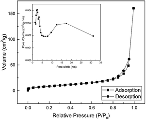 | ||
| Fig. 9 The Nitrogen adsorption–desorption isotherm and pore size distribution curves of SnO2 nanotube. | ||
The SnO2 nanotubes were assembled as a UV photosensor and were characterized for their current–voltage (I–V) character under UV light illumination. Fig. 10(a) represents room-temperature I–V characteristics under UV on/off in air conditions. The I–V curve of the fabricated nanotubes shows ohmic behavior and good photo-detection characteristics. Fig. 10(b) shows the sensitivities of the SnO2 nanotube UV sensor under 254 nm UV light. Response and recovery were both very fast, taking 14 and 11 seconds for 90% of full response and recovery, which are faster than those obtained in previous studies,48,49 respectively. This can be explained by the unique nanotube structure. As a principle of UV detector, we believe that the Schottky barrier generated by oxygen adsorption on the nanotube surface of SnO2 was destroyed by UV irradiations and the electricity flow was generated.49 In this process, oxygen adsorption/desorption is also one of the important factors. The larger surface to volume ratio makes the oxygen adsorption/desorption process easier. Therefore the large surface area to volume ratio and porous structure of the SnO2 nanotubes enhanced the performance of the UV photodetectors.
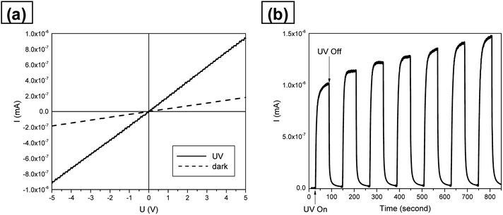 | ||
| Fig. 10 (a) Room-temperature I–V characteristics of the UV photodetector in air condition. (b) Sensitivities of the SnO2 nanotube UV photodetector under the exposure to 254 nm UV light. | ||
Conclusions
In this study, SnO2 nanotubes were successfully fabricated via template-free electrospinning and fine-controlled heat-treatment processes. By controlling the annealing temperature, the as-spun fiber transformed from a solid fiber to a partially filled and then a hollow-structured nanotube. It was found that at around 200 °C the PVB in the precursor fibers began to decompose and as the temperature was elevated to 400 °C, crystallized SnO2 shell began to form. Meanwhile, inside the fiber, accompanied by the gasification and oxidation of the organic components, tiny SnO2 nanoparticles would be produced and move to the shell to form larger grains at the shell, then the SnO2 nanotubes were formed. The as-prepared SnO2 nanotubes demonstrate good UV photodetection characteristics. The large surface area to volume ratio and porous structure made a faster response and recovery time, taking 14 and 11 seconds for 90% of full response and recovery, respectively.Conflicts of interest
There are no conflicts to declare.Notes and references
- L. Li, X. Yin, S. Liu, Y. Wang, L. Chen and T. Wang, Electrochem. Commun., 2010, 12, 1383–1386 CrossRef CAS.
- Z. Wen, Q. Wang, Q. Zhang and J. Li, Adv. Funct. Mater., 2007, 17, 2772–2778 CrossRef CAS.
- Y. Zhang, J. Li, G. An and X. He, Sens. Actuators, B, 2010, 144, 43–48 CrossRef CAS.
- H.-R. Kim, K.-I. Choi, J.-H. Lee and S. A. Akbar, Sens. Actuators, B, 2009, 136, 138–143 CrossRef CAS.
- S. B. Patil, P. P. Patil and M. A. More, Sens. Actuators, B, 2007, 125, 126–130 CrossRef CAS.
- C. A. Grimes, J. Mater. Chem., 2007, 17, 1451–1457 RSC.
- J. G. Lu, P. Chang and Z. Fan, Mater. Sci. Eng., R, 2006, 52, 49–91 CrossRef.
- D. V. Bavykin, V. N. Parmon, A. A. Lapkin and F. C. Walsh, J. Mater. Chem., 2004, 14, 3370–3377 RSC.
- A. Greiner and J. H. Wendorff, Angew. Chem., Int. Ed., 2007, 46, 5670–5703 CrossRef CAS PubMed.
- D. Li, J. T. McCann, Y. Xia and M. Marquez, J. Am. Ceram. Soc., 2006, 89, 1861–1869 CrossRef CAS.
- B. Ding, M. Wang, J. Yu and G. Sun, Sensors, 2009, 9, 1609–1624 CrossRef CAS PubMed.
- J. T. McCann, D. Li and Y. Xia, J. Mater. Chem., 2005, 15, 735 RSC.
- X. Xia, X. J. Dong, Q. F. Wei, Y. B. Cai and K. Y. Lu, Express Polym. Lett., 2012, 6, 169–176 CrossRef CAS.
- H. C. Zeng, J. Mater. Chem., 2006, 16, 649–662 RSC.
- Q. Zhang, W. Wang, J. Goebl and Y. Yin, Nano Today, 2009, 4, 494–507 CrossRef CAS.
- J.-S. Jang, S.-J. Kim, S.-J. Choi, N.-H. Kim, M. Hakim, A. Rothschild and I.-D. Kim, Nanoscale, 2015, 7, 16417–16426 RSC.
- J.-S. Jang, S.-J. Choi, S.-J. Kim, M. Hakim and I.-D. Kim, Adv. Funct. Mater., 2016, 26, 4740–4748 CrossRef CAS.
- H. Shan, C. B. Liu, L. Liu, J. B. Zhang, H. Y. Li, Z. Liu, X. B. Zhang, X. Q. Bo and X. Chi, ACS Appl. Mater. Interfaces, 2013, 5, 6376–6380 CrossRef CAS PubMed.
- Y. P. Huang, Y. E. Miao, L. S. Zhang, W. G. W. Tjiu, J. S. Pan and T. X. Liu, Nanoscale, 2014, 6, 10673–10679 RSC.
- J. S. Jang, S. J. Kim, S. J. Choi, N. H. Kim, M. Hakim, A. Rothschildc and I. D. Kim, Nanoscale, 2015, 7, 16417–16426 RSC.
- L. Xu, R. Q. Xing, J. Song, W. Xu and H. W. Song, J. Mater. Chem. C, 2013, 1, 2174–2182 RSC.
- B. Weng, F. Xu, G. Garza, M. Alcoutlabi, A. Salinas and K. Lozano, Polym. Eng. Sci., 2015, 55, 81–87 CrossRef CAS.
- F. Yener and O. Jirsak, J. Nanomater., 2012, 2012, 1–6 CrossRef.
- R. L. Feller, M. Curran, V. Colaluca, J. Bogaard and C. Bailie, Polym. Degrad. Stab., 2007, 92, 920–931 CrossRef CAS.
- S. Bai, W. Guo, J. Sun, J. Li, Y. Tian, A. Chen, R. Luo and D. Li, Sens. Actuators, B, 2016, 226, 96–103 CrossRef CAS.
- B. Lu, C. Zhu, Z. Zhang, W. Lan and E. Xie, J. Mater. Chem., 2012, 22, 1375–1379 RSC.
- R. Mukherjee, T. Chakrabarti, E. A. Anumol, T. A. Abinandanan and N. Ravishankar, ACS Nano, 2011, 5, 2700–2706 CrossRef CAS PubMed.
- W. Weng, J. Lin, Y. Du, X. Ge, X. Zhou and J. Bao, J. Mater. Chem. A, 2018, 6, 10168–10175 RSC.
- K. Zhang, X. Yang, Y. Wang, Y. Bing, L. Qiao, Z. Liang, S. Yu, Y. Zeng and W. Zheng, Sens. Actuators, B, 2017, 243, 465–474 CrossRef CAS.
- L. Xiao, S. Shu and S. Liu, Sens. Actuators, B, 2015, 221, 120–126 CrossRef CAS.
- H. C. Zeng, Curr. Nanosci., 2007, 3, 177–181 CrossRef CAS.
- X. Wallart, C. Henry de Villeneuve and P. Allongue, J. Am. Chem. Soc., 2005, 127, 7871–7878 CrossRef CAS PubMed.
- H.-T. Fang, C.-G. Liu, C. Liu, F. Li, M. Liu and H.-M. Cheng, Chem. Mater., 2004, 16, 5744–5750 CrossRef CAS.
- L. C. K. Liau and D. S. Viswanath, Ind. Eng. Chem. Res., 1998, 37, 49–57 CrossRef CAS.
- L. C. K. Liau, T. C. K. Yang and D. S. Viswanath, Appl. Spectrosc., 1996, 50, 1058–1065 CrossRef CAS.
- V. A. Matyshak and O. V. Krylov, Catal. Today, 1995, 25, 1–87 CrossRef CAS.
- J. Wu, D. Zeng, X. Wang, L. Zeng, Q. Huang, G. Tang and C. Xie, Langmuir, 2014, 30, 11183–11189 CrossRef CAS PubMed.
- J. D. Ambrósio, A. A. Lucas, H. Otaguro and L. C. Costa, Polym. Compos., 2011, 32, 776–785 CrossRef.
- C. Velásquez, F. Rojas, M. L. Ojeda, A. Ortiz and A. Campero, Nanotechnology, 2005, 16, 1278 CrossRef.
- M. Hajian, M. R. Reisi, G. A. Koohmareh and A. R. Zanjani Jam, J. Polym. Res., 2012, 19, 9966 CrossRef.
- F. Lian, Y. Wen, Y. Ren and H. Guan, J. Membr. Sci., 2014, 456, 42–48 CrossRef CAS.
- L. Costa, M. Avataneo, P. Bracco and V. Brunella, Polym. Degrad. Stab., 2002, 77, 503–510 CrossRef CAS.
- P. Zhang, L. Wang, X. Zhang, J. Hu and G. Shao, Nano-Micro Lett., 2015, 7, 86–95 CrossRef CAS PubMed.
- S. Cavaliere, I. Jiménez-Morales, G. Ercolano, I. Savych, D. Jones and J. Rozière, ChemElectroChem, 2015, 2, 1966–1973 CrossRef CAS.
- W. Q. Li, S. Y. Ma, Y. F. Li, X. B. Li, C. Y. Wang, X. H. Yang, L. Cheng, Y. Z. Mao, J. Luo, D. J. Gengzang, G. X. Wan and X. L. Xu, J. Alloys Compd., 2014, 605, 80–88 CrossRef CAS.
- J. S. Jang, S. J. Kim, S. J. Choi, N. H. Kim, M. Hakim, A. Rothschild and I. D. Kim, Nanoscale, 2015, 7, 16417–16426 RSC.
- W. Tang, J. Wang, Q. Qiao, Z. Liu and X. Li, J. Mater. Sci., 2015, 50, 2605–2615 CrossRef CAS.
- R. R. Kumar, K. N. Rao, K. Rajanna and A. R. Phani, Mater. Res. Bull., 2013, 48, 1545–1552 CrossRef CAS.
- L. Hu, J. Yan, M. Liao, L. Wu and X. Fang, Small, 2011, 7, 1012–1017 CrossRef CAS PubMed.
| This journal is © The Royal Society of Chemistry 2020 |

