
Comparison of organic and inorganic layers for structural templating of pentacene thin films†
Dong Kuk
Kim
a,
Daphné
Lubert-Perquel
ab and
Sandrine
Heutz
 *ab
*ab
aDepartment of Materials, Imperial College London, Prince Consort Road, London SW7 2BP, UK. E-mail: s.heutz@imperial.ac.uk
bLondon Centre for Nanotechnology, Imperial College London, Prince Consort Road, London SW7 2BP, UK
First published on 30th July 2019
Abstract
Pentacene is a key organic semiconductor, which has achieved prominence in transistor applications and as an archetypal material for singlet fission, the process whereby the absorption of one photon leads to the formation of two triplet states. Functional properties of molecules are highly anisotropic, and control over the molecular orientation in thin films with structural templating is commonly implemented as a route for governing the morphology and structure of organic films. Among the structural templating layers, 3,4,9,10-perylenetetracarboxylic dianhydride (PTCDA) and copper(I) iodide (CuI) have been shown to effectively template aromatic systems such as phthalocyanines. Here, we extend their use to pentacene thin films and find that a successful transition to a flat-lying arrangement is achieved with CuI films grown at high temperatures, but not with PTCDA. As a result, we postulate a model based on quadrupole interactions as the driving force behind the molecular orientation of pentacene. A 0.25 eV increase in work function and a two-fold increase in visible light absorption are recorded for the induced flat-lying orientation. Therefore, our templating methodology provides design opportunities for optoelectronic devices that require a predominantly flat-lying orientation.
New conceptsWe have developed a new methodology to produce highly ordered pentacene films growing in a flat-lying orientation, stable over thicknesses of over 200 nm, using CuI thin film templates. This is highly significant because pentacene is an archetypal molecular semiconductor with strongly anisotropic properties, and performance in e.g. solar cells is known to be more efficient in the flat-lying orientation. However, so far pentacene has been exclusively grown in a standing orientation, except in strained interfaces with e.g. a metal substrate where the strong interactions only produce a flat orientation in the first few monolayers before relaxation back to standing. By comparing with an ineffective molecular template, we are able to introduce a new mechanism for templating, based on the strong intermolecular quadrupole interactions, and their competition with the dipole induced by the polar substrate. Identifying this new driving force opens up materials engineering routes that can be applied to control the orientation and functional properties of a wide range of molecular systems to improve their performance in device applications. |
Introduction
Organic semiconductors have attracted significant attention over the years for their promising properties such as mechanical flexibility and affordability1 leading to an increase in possible applications such as transistors,2,3 photovoltaics4,5 and organic light-emitting diodes.6,7 These molecules can be synthetically tuned to complement the current performance thresholds of inorganic optoelectronic devices such as silicon-based transistors.8–10 Among these organic molecules, pentacene is a promising candidate which has been extensively researched for its physical properties, notably its charge transport and singlet fission properties,11–14 for optoelectronic applications.Pentacene is reported to grow in an upright orientation on non-interacting substrates, whereas a flat-lying arrangement up to a critical thickness of approximately 1.5 nm is observed on metal substrates followed by a structural reordering to an upright arrangement.15 The difference in molecular orientation is due to strong interactions such as charge transfer between the conjugated π-system of pentacene and the free electrons of the metal substrates.16 Molecular orientation plays a crucial role in the optimisation of the physical properties of pentacene for optoelectronic applications. For organic field-effect transistors (OFETs), the upright orientation is ideal since it provides a most favourable conduction channel between source and drain electrodes. However, for standard geometries of organic photovoltaic (OPV) devices, the charge is required to travel perpendicular to the substrate surface, which results in the upright arrangement being a considerable limitation. The impact of templating the pentacene molecules on the injection barrier has been well-documented with reports of a significant increase of ∼0.3–0.6 eV in the ionisation potential in the face-on orientation.17,18 In addition to considerations of molecular orientation, previous work found that in singlet fission, the geometry of the two inequivalent pentacene molecules influences the efficiency of triplet dissociation.19 Pentacene crystallises in a herringbone structure resulting in two configurations of nearest neighbour interactions: the herringbone pair and parallel pair. The former results in the triplets being trapped in a coupled state, whereas the latter dissociates into two free triplets that are optimal for charge generation in OPVs.
Structural templating is a commonly implemented approach for controlling the morphology and structure of organic thin films allowing further control over their electronic and optical properties.20,21 Extensive research has been conducted on the effect of both organic20,22–25 and inorganic layers26,27 on aromatic systems, most notably phthalocyanines. The similarities between planar phthalocyanines and pentacene originate from their aromaticity. Both have been reported to grow in a flat-lying manner on metals and an upright orientation on non-interacting substrates, suggesting the possibility of similar templating effects for the two molecules.28–31 Among the various templating layers, 3,4,9,10-perylenetetracarboxylic dianhydride (PTCDA) and copper(I) iodide (CuI) have been reported to successfully induce a flat-lying orientation for phthalocyanines.4,20,25,32,33 The driving force behind the successful templating effect of PTCDA is the π–π interactions with the phthalocyanine layer.25 Similar long-range order is reported for CuI,4,30 and has been linked to the preferential iodine termination at the surface,24,34 although no mechanism has been given. Consequently, the effect of both templating layers on the molecular orientation of pentacene is investigated here for the first time.
The crystal structure of PTCDA is well documented with the molecules reported to adopt a herringbone structure. PTCDA consists of two polymorphs, α and β, that align in a similar flat-lying manner along the (102) plane with the β-phase at a greater contact angle.35
CuI grows in three different crystalline phases: α, β and γ depending on temperature.36 At temperatures below 350 °C, CuI adopts the γ-phase and behaves as a large band gap p-type semiconductor or a p-type transparent conductor depending on doping.37 Vapour and solution processing methods have been used to produce highly crystalline CuI thin films for optoelectronic applications with the films adopting a (111) orientation at ambient temperatures on silicon substrates.38,39 CuI thin films at ambient temperatures were found to be highly disordered in the in-plane orientation causing the formation of two polymorphs of phthalocyanines, which both corresponded to a new orientation compared to the one on the bare substrate.4,27,40 Increased substrate temperatures were introduced to increase the CuI grain size allowing a more homogeneous growth of the inorganic layer. Thin films evaporated at 200 °C were reported to have an increased grain size with larger (111) faces due to the uniform out-of-plane orientation across the films.32 Thus, a more effective templating effect was observed on phthalocyanines.
In this work, we investigate the templating effect on pentacene of CuI thin films grown at two different substrate temperatures and of PTCDA thin films, with the aim to achieve a flat-lying molecular arrangement for a wider range of optoelectronic applications. We confirm that high substrate temperatures improve the crystallinity of the CuI thin films. Through surface characterisation of the bilayers, we find that the CuI thin films grown at high temperature induce a successful orientation transition of pentacene to a flat-lying arrangement, whereas the PTCDA film shows no evidence of promoting an orientation change. This contrast in templating effects helps develop a model relying on pentacene quadrupole interactions as the driving force that dominates the orientation of pentacene on polar substrates. We show the impact of this orientation change on the functional properties of the pentacene films by highlighting an increase in both the absorption cross-section and work function when moving from the standard upstanding geometry to the flat-lying orientation. Our work uncovers a new mechanism for molecular templating and provides opportunities to optimise functional properties for device applications that require a flat-lying orientation.
Experimental
Pentacene purified by sublimation was commercially obtained from TCI UK Ltd, CuI (98%) was supplied by Sigma Aldrich and PTCDA (97%) was supplied by Fluka. All were readily used with no further purification. The thin films were grown by organic molecular beam deposition (OMBD) in a Kurt J. Lesker Spectros 100 system at a base pressure of 3 × 10⁻⁷ mbar. All three materials were evaporated from separate Knudsen cells at a rate of 0.5 Å s−1 on silicon, quartz and glass substrates. This rate was chosen as it is the highest rate at which the bulk phase is minimised compared to the desired thin film phase, based on our previous work on non-templated films.41 The film thicknesses and rates were monitored using quartz crystal microbalance sensors placed near the sources and substrates. The substrates were either kept at room temperature during deposition, or heated using quartz lamps, with the temperature monitored by a thermocouple placed near the substrate.Surface characterisation of the films was carried out using tapping mode atomic force microscopy (AFM) on the Naio-Nanosurf microscope and Asylum Research MFP-3D microscope. All roughness values were determined using the root mean square roughness (RRMS) of the total window of the AFM images, using the open-source software Gwyddion.42 The reported RRMS is taken as the average over three separate areas of the image with the standard deviation quoted as an error. The lateral grain size as a function of growth temperature was calculated from the AFM images using watershed to mark the grain boundaries. Electrical surface characterisation of the films was carried out using kelvin probe force microscopy (KPFM) on the Asylum Research MFP-3D microscope. The work function of the conductive tip was determined to be 4.82 eV by scanning a reference sample (HOPG) of known work function (4.60 eV).43 The contact potential difference of each sample was determined using a Gaussian distribution fitting.
Cross-section images of the samples were taken using scanning electron microscopy (SEM) on a Zeiss LEO Gemini 1525 microscope. All samples were coated in a 10 nm conductive layer of chromium and grounded to the sample holder with silver paste.
X-ray diffraction (XRD) scans in the fixed θ–2θ geometry were conducted on a Philips X’Pert Pro Panalytical using a Cu Kα source (λ = 1.5406 Å) at a current of 40 A and voltage of 40 V. Texture measurements were carried out by conducting pole figure scans by rotating the sample along the ϕ axis at ψ angles set at regular intervals44 and were carried out on a Philips X’Pert Panalytical diffractometer. The crystal structure and molecular orientations were examined with the open-source software Mercury.45
Transmittance scans were conducted using ultraviolet-visible spectroscopy (UV-vis) on an Agilent Technologies Cary 5000 UV-vis-NIR spectrophotometer in an integrating sphere configuration over a wavelength range of 200 nm to 800 nm.
Results and discussion
Single layers
Pentacene films with a thickness of 200 nm were deposited on silicon, quartz and glass substrates. The topography and grain size were discovered to be substrate-dependent (Fig. 1a–c), with average roughness values of 12.9 ± 0.2 nm, 8.5 ± 1.0 nm and 4.8 ± 0.2 nm for silicon, quartz and glass respectively. The pentacene films deposited on silicon consist of irregularly shaped crystals with an average size of 397 ± 196 nm (Fig. 1a), which is in good agreement with the literature.41,46 The error on the lateral grain size, given as a standard deviation, is significant, representing a wide size distribution and the limitations of grain boundary determination due to the close proximity of the grains. The greater roughness of the films deposited on the silicon substrates can be attributed to the larger crystals. The topography of the films deposited on quartz also consists of irregularly shaped crystals but with a reduced grain size of 211 ± 84 nm (Fig. 1b). However, a high homogeneity and consistent grain size of 155 ± 49 nm is observed for the pentacene film deposited on glass (Fig. 1c). The differences in the roughness values and topography can be related to the varying interatomic interactions between the film and substrate. Higher molecular mobility on the silicon allows crystallisation of the pentacene into larger domains.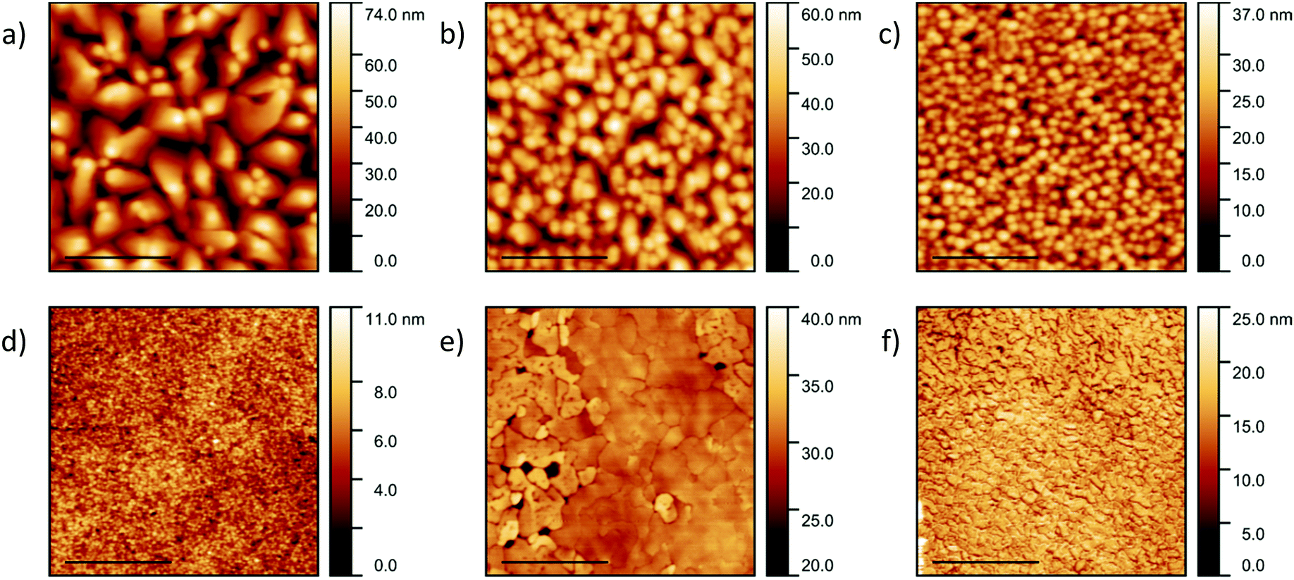 | ||
| Fig. 1 AFM images of 200 nm pentacene films grown on (a) silicon, (b) quartz and (c) glass and CuI films grown on silicon at (d) 20 nm at 20 °C, (e) 50 nm at 200 °C and (f) 100 nm at 200 °C. The scale bar is set at 2 μm. | ||
CuI films with a thickness of 20 nm were also deposited on the three substrates at room temperature. No significant differences in topography and roughness were observed suggesting the CuI film to be substrate-independent (Fig. S1, ESI†). As a result, for convenience the subsequent CuI films were only deposited on silicon substrates. Grain sizes of 69 ± 35 nm were observed agreeing well with the literature describing the formation of smooth layers at room temperature (Fig. 1d).47 At 200 °C, CuI is known to form discontinuous layers due to an island growth32 and therefore to ensure full coverage of the substrate, the film was initially grown to a thickness of 50 nm. Although larger gain sizes were observed, pinholes were visible in the film indicating incomplete layer growth (Fig. 1e). As a result, the subsequent films were evaporated to a thickness of 100 nm where no pinholes were evident with grain sizes of 72 ± 42 nm (Fig. 1f). The roughness values of the films at room temperature and 200 °C were recorded as 1.3 ± 0.1 nm and 5.1 ± 0.8 nm respectively. The increase in roughness is due to the significantly larger grains at 200 °C. The determined values were compared to the out-of-plane grain sizes calculated from XRD discussed below.
XRD was used to identify the crystal structure of the films. A highly ordered structure is observed in the pure pentacene film on the silicon substrate (Fig. 2a). The (00l) planes dominate the XRD pattern confirming that the molecules orient in a nearly perpendicular manner to the substrate surface as observed previously.28 Previous work has reported the 0.5 Å s−1 deposition rate forms films consisting of two pentacene polymorphs: thin film phase and bulk phase.41 In the dominant thin film phase, the two inequivalent pentacene molecules align to the substrate surface at angles of 86.6° and 88.7°.28 High crystallinity and texture is also observed in the CuI film at both room temperature and 200 °C with the XRD pattern consisting of the (111) plane with a minor contribution from the higher order (222) plane indicative of long range order (Fig. 2b).48 With increasing substrate temperature, the intensity of the (111) plane significantly increases with the full width half maximum (FWHM) decreasing from 2θ = 0.47° to 0.22° for the growth on substrates at room temperature and 200 °C respectively.32 The corresponding out-of-plane grain sizes calculated using the Scherrer equation are 18.3 ± 0.1 nm and 39.4 ± 0.3 nm respectively. The grain size increases with increasing temperature which confirms larger island growth as observed using AFM. The out-of-plane values are a factor of two smaller than the lateral sizes which may be due to contribution of an amorphous fraction to the grains, crystal anisotropy or limitations in the ability to resolve individual grains in the AFM images.
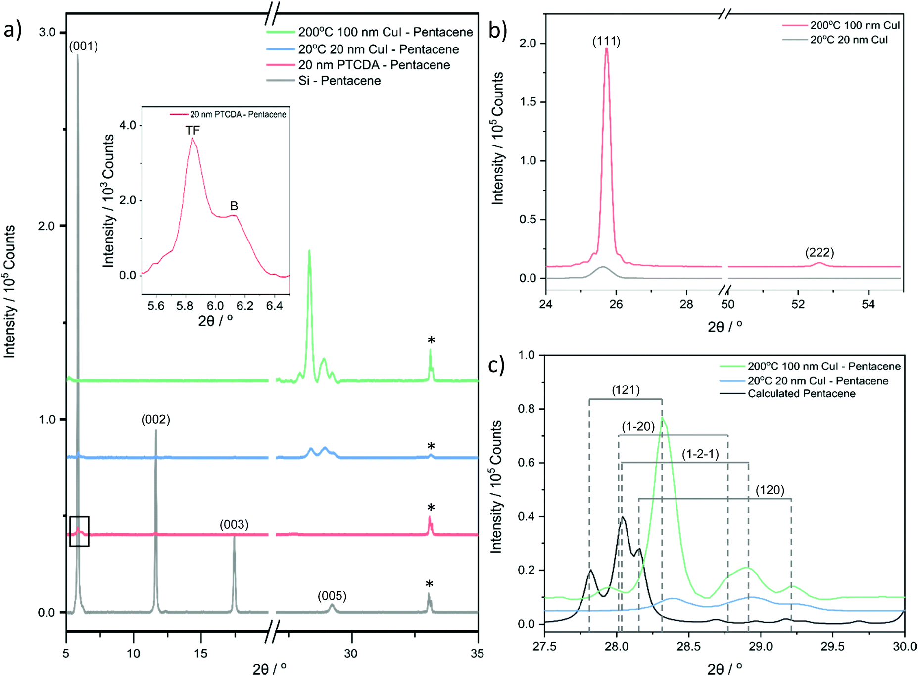 | ||
| Fig. 2 (a) Diffraction patterns of 200 nm pentacene films deposited on silicon, PTCDA, room temperature CuI and 200 °C CuI. The inset presents the thin film phase and bulk phase of pentacene present on PTCDA labelled TF and B respectively. (b) Diffraction patterns of CuI films grown at the two growth temperatures showing a significant increase in intensity of the (111) plane at 200 °C. (c) A close-up of the CuI templated pentacene films presenting the four additional peaks, (121), (1−2−1), (1−20) and (120) observed with the pentacene powder diffraction pattern (CCDC 665900).26 The silicon substrate peak is identified with *. The diffraction scans in (a) are stacked at regular intervals of 4 × 10⁴ counts. The diffraction scans in (b) are stacked at 5 × 10³ counts and the diffraction scans in (c) are stacked at 5 × 10³ counts. The 2θ offsets of the four additional peaks are presented in (c). | ||
Templated bilayers
The templating effect of the CuI films and PTCDA film was compared. The PTCDA-templated pentacene film presents no evidence of a significant orientation change as only the characteristic (001) and (002) pentacene peaks are observed, albeit at significantly lower intensities (Fig. 2a). The inset in Fig. 2a shows that the intensity of the (001) plane of the thin film phase (TF) of pentacene is suppressed with an enhanced contribution from the bulk phase (B) of pentacene. As the bulk phase peak was reported to appear at an angle ψ = 5°,41,49 this suggests that the pentacene molecules have a mosaicity that extends over a range of at least 5° as a result of the PTCDA underlayer. On the other hand, both CuI-templated pentacene films show a transition to a new molecular orientation with the presence of three additional planes in the region 2θ = 27–30°. These cannot be directly attributed to known polymorphs of pentacene or to the unpurified powder used as the source material (Fig. S2, ESI†), due to non-systematic shifts of 2θ = 0.5–1° in peak position. However, it should be noted that in all cases, this region is characteristic of planes which are nearly parallel to at least one pentacene molecule. It is possible that the shifts are due to strain slightly modifying the lattice parameters of the polymorph that is most likely to form in the growth conditions employed, i.e. the thin film phase.26 We therefore attribute the peaks at 2θ = 28.3°, 28.9° and 29.2° to the (121), (1−2−1) and (120) planes respectively, as shown in Fig. 2c, and note that full structure redetermination is beyond the scope of this work. Within the framework of the thin film phase, due to the herringbone structure, one of the two pentacene molecules aligns strongly along the (120) and (121) planes at angles of 8.23° and 8.20° respectively (Fig. 3a and b) with the other inequivalent molecule aligning to the (1−2−1) plane at an angle of 8.23° (Fig. 3c). On the room temperature CuI film, the (001) plane characteristic of the upright growth of pentacene is still present though at reduced intensities indicating an incomplete templating effect (Fig. 2a). In contrast, a complete templating effect is observed for the 200 °C CuI templating layer with the (121), (120) and (1−2−1) plane intensities significantly amplified similar to that of the CuI (111) peak. In addition to the three planes observed on the 200 °C CuI templated pentacene film, an additional peak corresponding to the (1−20) plane is present as a shoulder on the (1−2−1) plane for room temperature growth. Similar to the (1−2−1) plane, the other inequivalent pentacene molecule is aligned to the (1−20) plane at an angle of 8.64° (Fig. 3d). To compare the peak intensities of the (121) plane of both CuI templated pentacene films, the texture factor ζ is used to normalise the experimental intensities based on the powder configuration of pentacene intensities from the literature.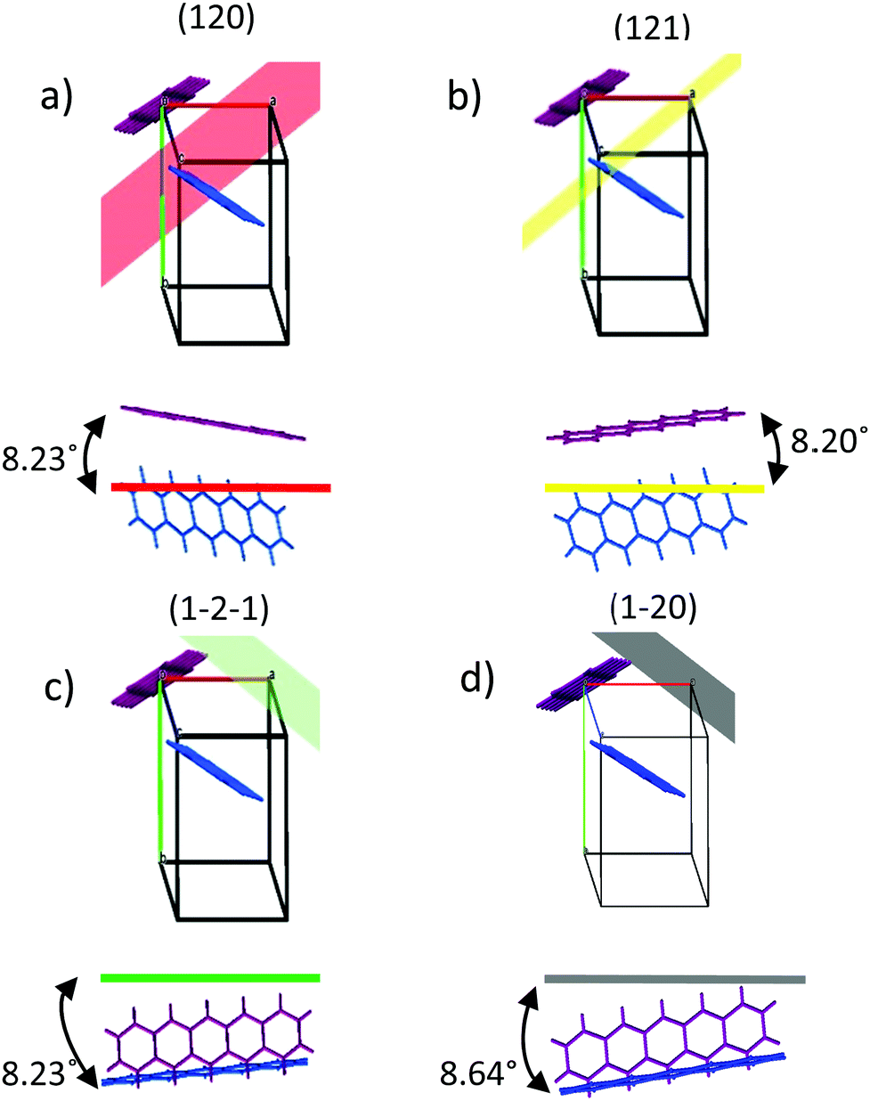 | ||
| Fig. 3 Molecular orientation of the pentacene dimer along (a) (120), (b) (121), (c) (1−2−1) and (d) (1−20). The pentacene dimers are colour coded to distinguish which molecule aligns to the three planes. The purple pentacene molecule orientates in a flat-lying manner along the (120) and (121) planes whilst the blue pentacene molecule orientates in a flat-lying manner along the (1−2−1) and (1−20) planes. The (1−20) plane is only observed on the 200 °C CuI templated pentacene film. | ||
This is given by:50
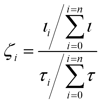
The texture factors of the pentacene film templated by 20 °C CuI and 200 °C CuI are presented in Table 1. This indicates that the 200 °C CuI-templated pentacene film is predominantly aligned along the (121) plane, where the pentacene molecules are at an angle of 8.20°. This is the smallest angle amongst the four planes suggesting the presence of stronger interatomic interactions at the bilayer interface compared to those of the room temperature CuI–pentacene bilayer. For both CuI templated pentacene films, the (120) plane is strongly suppressed compared to the literature (Fig. 2c).
| Pentacene template | Crystal planes | ||
|---|---|---|---|
| (121) | (1−2−1) | (120) | |
| 20 °C 20 nm CuI | 1.66 | 0.93 | 0.62 |
| 200 °C 100 nm CuI | 3.57 | 0.30 | 0.16 |
XRD patterns of the CuI templated films provides information on the additional crystal planes but no quantitative information on the level of texture along these new planes. A pole figure scan was taken on the 200 °C CuI templated pentacene film to determine the overall orientation distribution of the pentacene molecules with respect to the (121) plane (Fig. 4). A single peak is observed at the centre of the pole figure confirming the (121) plane to align parallel to the substrate surface. The peak has an FWHM of 8° which suggests a minimal deviation of the preferred orientation of the pentacene molecules. The (120) and (1−2−1) planes are found at tilt angles of 11.85° and 64.90° respectively relative to the (121) plane. This suggests that any contributions from the (120) plane would be at the periphery of the singular peak, whilst contributions from the (1−2−1) plane would be around the ψ = 65° region of the pole figure. However, based on the texture factor calculations (Table 1), the number of pentacene crystals aligned along the (1−2−1) and (120) planes are found to be 10 times and 20 times lower compared to those along the (121) plane. Thus, the contributions of both planes fall below the background levels of the pole figure scan. Due to the lower resolution of the diffractometer, the pole figures of the (120) and (1−2−1) peaks could not be observed. Any possible para-crystalline contributions cannot be detected using conventional XRD-based characterisation techniques, but could be identified using spectroscopic methods that are sensitive to molecular orientation even in the absence of long-range order.19,51
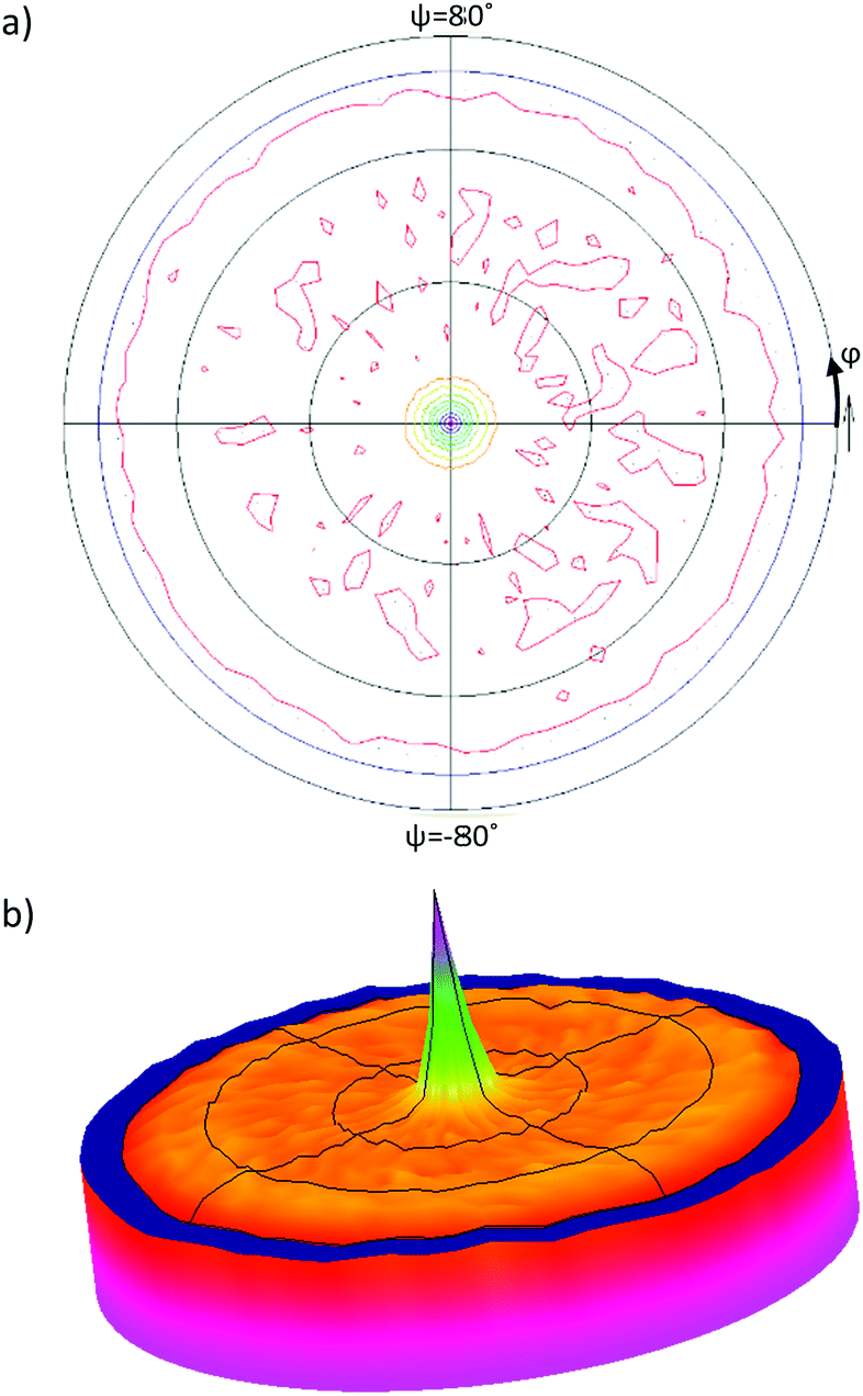 | ||
| Fig. 4 Pole figure scan of the pentacene film templated by CuI grown at 200 °C aligned to the (121) plane at 2θ = 28.3°. (a) 2D representation and (b) 2.5D representation. The pole figure scan consists of ϕ scans of 360° taken over a ψ angle range of −80° to 80° at a step size of 5°. | ||
The AFM images of the templated films are presented in Fig. 5 and the roughness and lateral grain sizes presented in Table 2. A homogeneous film with an average grain size of 134 ± 57 nm is observed for the PTCDA-templated pentacene film (Fig. 5a). The pentacene film templated by the CuI film grown at room temperature consists of grains with a mean grain size of 136 ± 56 nm (Fig. 5b). This is approximately half the size of those of pentacene deposited directly on silicon. A smaller grain size of 103 ± 46 nm is observed for the pentacene film templated by the CuI film grown at 200 °C (Fig. 5c). The smaller grain sizes for the templated films, especially compared to deposition onto a silicon substrate, is due to the pentacene molecules aligning predominantly parallel to the (121) plane, with most effective π–π stacking and crystal growth normal to the substrate. The out-of-plane grain size calculated from the XRD patterns increases from 31.6 ± 2.3 nm to 48.9 ± 2.6 nm following templating, which is inversely correlated to the decrease in lateral size. However due to the large spread in sizes and limitations of the Scherrer equation for anisotropic crystals this trend is not conclusive. In comparison with the pentacene film on silicon, the z-scale of the CuI templated pentacene films is significantly greater. This is again due to the plate-like crystals of pentacene (Fig. 1a) undergoing an approximate 90° tilt to a parallel orientation which results in the grains stacking perpendicularly to the substrate surface. The cross-section images of the templated pentacene films provide further visualisation of the pentacene grains undergoing a rotation to the stacking axis perpendicular to the substrate surface (Fig. S3, ESI†).
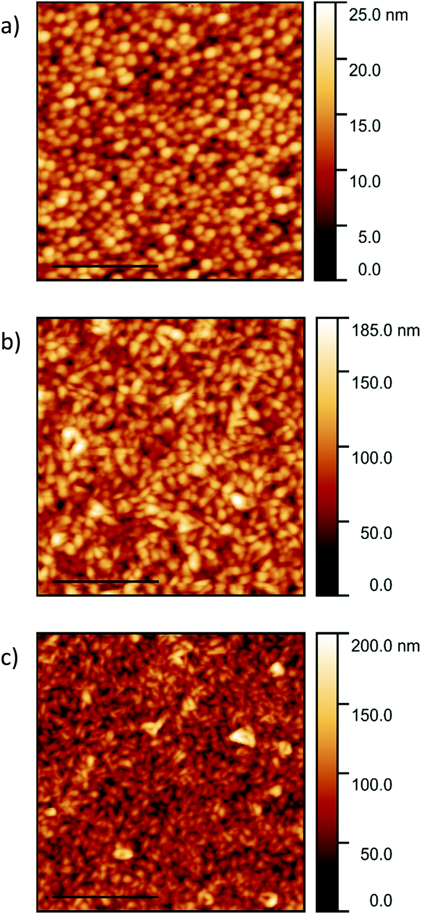 | ||
| Fig. 5 AFM images of 200 nm pentacene films templated by (a) 20 nm PTCDA, (b) 20 nm CuI grown at room temperature and (c) 100 nm CuI grown at 200 °C. The scale bars are set to 2 μm. | ||
| Pentacene substrate | Roughness (nm) | Lateral grain size (nm) |
|---|---|---|
| Silicon | 12.9 ± 0.2 | 397 ± 196 |
| Quartz | 8.5 ± 1.0 | 211 ± 84 |
| Glass | 4.8 ± 0.2 | 155 ± 49 |
| 20 nm PTCDA | 3.1 ± 0.3 | 134 ± 57 |
| 20 °C 20 nm CuI | 22.5 ± 1.1 | 136 ± 56 |
| 200 °C 100 nm CuI | 23.4 ± 1.3 | 103 ± 46 |
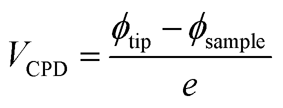
Contact potential difference signals of the samples when performing AFM measurements provides information on the film work function, by recording the difference between the sample and conductive tip shown in the following equation:52
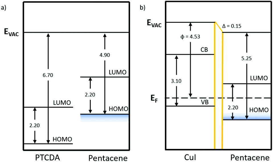 | ||
| Fig. 6 Energy level diagrams of the pentacene/PTCDA and pentacene/CuI bilayers with the band gap and ionisation potential values taken from the literature.17,37,65 The work function values were experimentally determined using KPFM. The area shaded in blue represents the range of ionisation potentials depending on orientation. | ||
In addition to examining the structural and electronic implications of introducing the templating layers, the effect on the optical properties of pentacene was also investigated. The UV-vis absorption spectra of the various templated samples are presented in Fig. S5, ESI.† The PTCDA-templated pentacene film absorption spectrum is nearly identical to that of the pure pentacene film which confirms that PTCDA is not effective as a structural template for pentacene. The room temperature CuI-templated pentacene film absorption spectrum also presents a similar spectrum to that of the pure pentacene film with a minimal increase in absorption. This may be due to competing interactions between the pentacene molecules maintaining the preferential upright orientation and transitioning to the new flat-lying orientation. In contrast to the former two templated films, an approximate two-fold increase in absorption is observed for the 200 °C CuI-templated pentacene film. This is attributed to the increased absorption cross-section as a result of the induced flat-lying molecular orientation and thus supports the benefits of templating for OPV applications.
The interatomic interactions between the two types of templating layers and pentacene layer differ greatly. Simulation work57 on a pentacene/PTCDA interface found multiple competing effects. On one hand, the interatomic interactions between the conjugated π-system of pentacene and the aromatic system of PTCDA as well as H-bonding between the oxygens of the dianhydride with the H-groups of pentacene act in favour of templating. On the other hand, the preservation of the bulk properties of the pentacene crystal acts against the overall change in orientation. The theoretical work showed that at the interface along the crystal planes of interest, (001) of pentacene and (102) of PTCDA respectively, both molecules were found to retain their bulk structure. This is in agreement with Sehati et al.,58 who found the orientation change to a flat-lying arrangement to be costly in energy.
On the other hand, in CuI films grown on silicon substrates, grains with either Cu+ and I− terminations have been reported to be present.26 Along the (111) plane of thin films, the I− termination is energetically preferred to the Cu+ termination suggesting that the surface consists of a high electron density, which results in a weak dipole normal to the surface.34 Theoretical calculations of the partial charges of pentacene have shown the plane of the aromatic system to be negatively charged, whilst the peripheral hydrogen groups are positively charged.59 The partial charge distribution suggests that pentacene molecules should adopt a perpendicular arrangement on the CuI substrate to minimise any strong repulsive interactions with the negatively charged molecular ring (Fig. 7a). Therefore, purely electrostatic interactions cannot be used to rationalise the experimental results of a flat-lying orientation. Furthermore, purely dipolar interactions between the layers have been discarded as a possible explanation behind the observed orientation transition. Indeed, electronic density simulations have determined that pentacene molecules have anisotropic polarisability along their x-direction.60,61 Thus, induced dipole–dipole interactions across the pentacene–CuI interface would result in the pentacene molecules preferentially orientating perpendicularly on the CuI layer (Fig. 7a), with parallel intermolecular dipoles. However, this would lead to a frustration of the quadrupole interactions between the adjacent molecules, which are found to be a significant force in determining its stable structure, and is therefore not observed.59 The importance of quadrupole interactions in the self-assembly of organic aromatic systems has been well-documented,62,63 and we assign this interaction as the dominant driving force behind the mechanism for the templating of CuI. Indeed, if the pentacene molecules adopt a flat-lying orientation onto CuI, the induced dipole–dipole interaction is no longer aligned with the x-direction, and the quadrupole interactions can be maintained. This would result in the herringbone structure being maintained for all pentacene layers which is in agreement with the experimental results presented here (Fig. 7c and d). The varying molecular tilt angles of pentacene indicate an interplay between bulk intermolecular interactions and molecule–substrate interactions.64 The herringbone structure of pentacene balances the repulsive forces between the negatively charged aromatic plane and CuI surface with the attractive interactions between the peripheral positively charged hydrogen groups of pentacene and CuI surface (Fig. 7d). This interaction model is supported by the ineffectiveness of PTCDA as a templating layer for pentacene, which can be explained by the absence of dipole interactions between the pentacene and PTCDA layers. The importance of the quadrupole interactions is also consistent with the upright orientation of the pentacene molecules on non-interacting substrates as this configuration maximises the dominant intermolecular interactions from the onset of film formation, and allows the thermodynamically favourable structure to proceed (Fig. 7b).
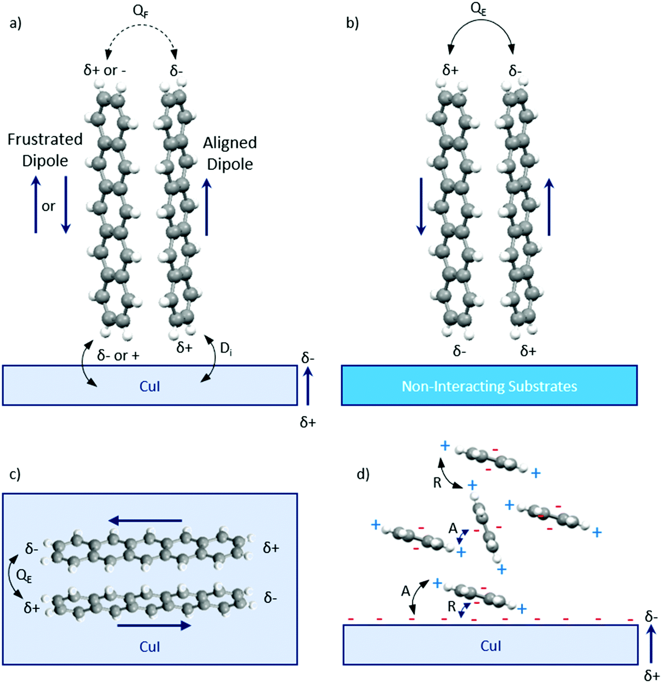 | ||
| Fig. 7 Schematic diagram of the dominant interactions between the pentacene molecules and substrate. (a) An upright structure is not predicted on CuI due to the anisotropic polarisability of pentacene along its x-direction and the arising frustration to maintain quadrupole interactions. (b) Pentacene adopts the herringbone structure on non-interacting substrates such as silicon due to the dominant quadrupole coupling between the molecules. (c) A top view of the flat-lying herringbone structure observed from the experimental results due to a balance between the intermolecular quadrupole coupling between the pentacene molecules and dipole-induced dipole interactions with CuI. (d) A front view of the flat-lying herringbone structure observed on CuI. QF represents the frustrated quadrupole interaction, QE represents the equilibrium quadrupole interaction and Di represents the induced dipole interaction. A and R represent the attractive and repulsive interactions between the pentacene partial charges and negatively charged CuI surface. | ||
Conclusions
We have successfully induced a flat-lying pentacene orientation using CuI as a templating layer, with an unprecedented long-range texture extending through at least 200 nm pentacene thickness. The PTCDA-templated pentacene film showed no orientation transition to a flat-lying arrangement and was concluded to be an ineffective templating layer for pentacene thin films. For the CuI films, optimised through growth at high substrate temperature, the pentacene standing orientation is entirely supressed. Additional diffraction planes in the region 2θ = 27–30° correspond to pentacene molecules oriented with an angle of approximately 8° to the substrate, and the strong preferential orientation is confirmed by pole figure analysis. The origin of the interfacial interactions between substrate and pentacene has been discussed by comparing the successful template CuI with the ineffective PTCDA. We have proposed a model identifying quadrupole interactions as the possible driving force behind the successful templating effect of CuI. This new mechanism should significantly broaden the range of orientations that can be obtained in molecular thin films, especially considering that quadrupole intermolecular interactions are dominant in a wide range of functional aromatic molecules.62,63 Our findings complement previous templating mechanisms, including π–π interactions,25,65 hydrogen bonds66 and charge transfer,16 which have been found to be ineffective with pentacene.This new molecular orientation provides application opportunities for fission and OPV devices as the upright orientation of pentacene was a severe limitation of device performance. Furthermore, the introduction of CuI encourages charge transport throughout the bilayer due to favourable energy level alignments. The manipulation of the work function provides insight into the interfacial electronic effects from introducing the CuI layer. These properties allow new device architectures to be explored to enhance organic device performances.
Conflicts of interest
There are no conflicts to declare.Acknowledgements
DK acknowledges the Department of Materials at Imperial College London for a PhD studentship. DLP acknowledges a PhD studentship from the EPSRC Centre of Doctoral Training for the Advanced Characterisation of Materials (EP/L015277/1). We thank Richard Sweeney for assistance in the XRD measurements.Notes and references
- C. D. Dimitrakopoulos and P. R. L. Malenfant, Adv. Mater., 2002, 14, 99–117 CrossRef CAS.
- B. Gunduz, O. A. Al-Hartomy, S. A. F. Al Said, A. A. Al-Ghamdi and F. Yakuphanoglu, Synth. Met., 2013, 179, 94–115 CrossRef CAS.
- S. Tanaka, H. Yanagisawa, M. Iizuka, M. Nakamura and K. Kudo, Electr. Eng. Jpn., 2004, 149, 43–48 CrossRef.
- B. P. Rand, D. Cheyns, K. Vasseur, N. C. Giebink, S. Mothy, Y. Yi, V. Coropceanu, D. Beljonne, J. Cornil, J. L. Brédas and J. Genoe, Adv. Funct. Mater., 2012, 22, 2987–2995 CrossRef CAS.
- J. Yu, Y. Zheng and J. Huang, Polymers, 2014, 6, 2473–2509 CrossRef.
- B. Minaev, G. Baryshnikov and H. Agren, Phys. Chem. Chem. Phys., 2014, 16, 1719–1758 RSC.
- S. Ho, S. Liu, Y. Chen and F. So, J. Photonics Energy, 2015, 5, 057611 CrossRef.
- S. F. Nelson, Y. Y. Lin, D. J. Gundlach and T. N. Jackson, Appl. Phys. Lett., 1998, 72, 1854–1856 CrossRef CAS.
- J. Tarver, J. E. Yoo and Y. L. Loo, Comprehensive Nanoscience and Technology, 2011, pp. 413–446 Search PubMed.
- O. Ostroverkhova and O. D. Jurchescu, Handbook of Organic Materials for Optical and (Opto)electronic Devices, Woodhead Publishing, 2013, pp. 377–397 Search PubMed.
- J. Lee, P. Jadhav, P. D. Reusswig, S. R. Yost, N. J. Thompson, D. N. Congreve, E. Hontz, T. Van Voorhis and M. A. Baldo, Acc. Chem. Res., 2013, 46, 1300–1311 CrossRef CAS PubMed.
- P. M. Zimmerman, Z. Zhang and C. B. Musgrave, Nat. Chem., 2010, 2, 648–652 CrossRef CAS PubMed.
- P. M. Zimmerman, F. Bell, D. Casanova and M. Head-Gordon, J. Am. Chem. Soc., 2011, 133, 19944–19952 CrossRef CAS PubMed.
- A. A. Günther, J. Widmer, D. Kasemann and K. Leo, Appl. Phys. Lett., 2015, 106, 233301 CrossRef.
- S. Lukas, S. Söhnchen, G. Witte and C. Wöll, ChemPhysChem, 2004, 5, 266–270 CrossRef CAS PubMed.
- E. Umbach, M. Sokolowski and R. Fink, Appl. Phys. A: Mater. Sci. Process., 1996, 63, 565–576 CrossRef CAS.
- X. Liu, A. Grüneis, D. Haberer, A. V. Fedorov, O. Vilkov, W. Strupinski and T. Pichler, J. Phys. Chem. C, 2013, 117, 3969–3975 CrossRef CAS.
- T. Nishi, M. Kanno, M. Kuribayashi, Y. Nishida, S. Hattori, H. Kobayashi, F. von Wrochem, V. Rodin, G. Nelles and S. Tomiya, Appl. Phys. Lett., 2018, 113, 163302 CrossRef.
- D. Lubert-Perquel, E. Salvadori, M. Dyson, P. N. Stavrinou, R. Montis, H. Nagashima, Y. Kobori, S. Heutz and C. W. M. Kay, Nat. Commun., 2018, 9, 4222 CrossRef.
- S. Heutz, C. Mitra, W. Wu, A. J. Fisher, A. Kerridge, M. Stoneham, T. H. Harker, J. Gardener, H. H. Tseng, T. S. Jones, C. Renner and G. Aeppli, Adv. Mater., 2007, 19, 3618–3622 CrossRef CAS.
- B. Verreet, R. Müller, B. P. Rand, K. Vasseur and P. Heremans, Org. Electron., 2011, 12, 2131–2139 CrossRef CAS.
- W. S. Hu, Y. T. Tao, Y. J. Hsu, D. H. Wei and Y. S. Wu, Langmuir, 2005, 21, 2260–2266 CrossRef CAS PubMed.
- D. Käfer, L. Ruppel and G. Witte, Phys. Rev. B: Condens. Matter Mater. Phys., 2007, 75, 085309 CrossRef.
- X. Liu, Y. Zhan, S. Braun, F. Li and M. Fahlman, Phys. Rev. B: Condens. Matter Mater. Phys., 2009, 80, 115401 CrossRef.
- S. Heutz, R. Cloots and T. S. Jones, Appl. Phys. Lett., 2000, 77, 3938–3940 CrossRef CAS.
- A. J. Ramadan, I. Hancox, S. Huband, C. C. Parkins, S. A. F. Bon, M. Walker, S. Fearn, C. F. McConville, T. S. Jones and L. A. Rochford, J. Phys. Chem. C, 2016, 120, 4448–4452 CrossRef CAS.
- L. A. Rochford, A. J. Ramadan, S. Heutz and T. S. Jones, Phys. Chem. Chem. Phys., 2014, 16, 25404–25408 RSC.
- S. Schiefer, M. Huth, A. Dobrinevski and B. Nickel, J. Am. Chem. Soc., 2007, 129, 10316–10317 CrossRef CAS PubMed.
- M.-C. Lu, R.-B. Wang, A. Yang and S. Duhm, J. Phys.: Condens. Matter, 2016, 28, 94005 CrossRef PubMed.
- S. Kera, M. B. Casu, K. R. Bauchspieß, D. Batchelor, T. Schmidt and E. Umbach, Surf. Sci., 2006, 600, 1077–1084 CrossRef CAS.
- A. Ruocco, F. Evangelista, A. Attili, M. P. Donzello, M. G. Betti, L. Giovanelli and R. Gotter, J. Electron Spectrosc. Relat. Phenom., 2004, 137–140, 165–169 CrossRef CAS.
- L. A. Rochford, D. S. Keeble, O. J. Holmes, G. J. Clarkson and T. S. Jones, J. Mater. Chem. C, 2014, 2, 6056–6060 RSC.
- K. Yamada and K. Nakayama, J. Electrochem. Soc., 2019, 166, B3103–B3108 CrossRef CAS.
- A. S. Bhalla and E. W. White, Acta Crystallogr., Sect. B: Struct. Crystallogr. Cryst. Chem., 1971, 27, 852–853 CrossRef CAS.
- T. Ogawa, K. Kuwamoto, S. Isoda, T. Kobayashi and N. Karl, Acta Crystallogr., Sect. B: Struct. Sci., 1999, 55, 123–130 CrossRef.
- D. A. Keen and S. Hull, J. Phys.: Condens. Matter, 1995, 7, 5793–5804 CrossRef CAS.
- M. N. Amalina, Y. Azilawati, N. A. Rasheid and M. Rusop, Procedia Eng., 2013, 56, 731–736 CrossRef CAS.
- A. Liu, H. Zhu, W. T. Park, S. J. Kang, Y. Xu, M. G. Kim and Y. Y. Noh, Adv. Mater., 2018, 30, 1802379 CrossRef PubMed.
- C. Yang, M. Kneiß, M. Lorenz and M. Grundmann, Proc. Natl. Acad. Sci. U. S. A., 2016, 113, 12929–12933 CrossRef CAS.
- L. A. Rochford, A. J. Ramadan, D. S. Keeble, M. P. Ryan, S. Heutz and T. S. Jones, Adv. Mater. Interfaces, 2015, 2, 1–4 Search PubMed.
- D. Lubert-Perquel, D. Kim, P. Robaschik, C. Kay and S. Heutz, J. Mater. Chem. C, 2019, 7, 289–296 RSC.
- D. Nečas and P. Klapetek, Cent. Eur. J. Phys., 2012, 10, 181–188 Search PubMed.
- W. Melitz, J. Shen, S. Lee, J. S. Lee, A. C. Kummel, R. Droopad and E. T. Yu, J. Appl. Phys., 2010, 108, 023711 CrossRef.
- B. D. Cullity, Elements of X-ray Diffraction, Addison-Wesley Publishing Company Inc., Boston, 1956 Search PubMed.
- C. F. Macrae, P. R. Edgington, P. McCabe, E. Pidcock, G. P. Shields, R. Taylor, M. Towler and J. Van De Streek, J. Appl. Crystallogr., 2006, 39, 453–457 CrossRef CAS.
- H. Yanagisawa, T. Tamaki, M. Nakamura and K. Kudo, Thin Solid Films, 2004, 464, 398–402 CrossRef.
- X. Chen, X. Wei, H. Zhang and J. Wang, Phys. Status Solidi A, 2017, 214, 1700064 CrossRef.
- R. W. G. Wyckoff and E. Posnjak, J. Am. Chem. Soc., 1922, 44, 30–36 CrossRef CAS.
- T. Siegrist, C. Besnard, S. Haas, M. Schiltz, P. Pattison, D. Chernyshov, B. Batlogg and C. Kloc, Adv. Mater., 2007, 19, 2079–2082 CrossRef CAS.
- C. Barrett and T. Massalski, Structure of Metals: Crystallographic Methods, Principles and Data, Pergamon Press Ltd, Oxford, 3rd rev., 1980 Search PubMed.
- A. Girlando, M. Masino, A. Brillante, T. Toccoli and S. Iannotta, Crystals, 2016, 6, 41 CrossRef.
- W. Melitz, J. Shen, A. C. Kummel and S. Lee, Surf. Sci. Rep., 2011, 66, 1–27 CrossRef CAS.
- J. Q. Zhong, H. Y. Mao, R. Wang, D. C. Qi, L. Cao, Y. Z. Wang and W. Chen, J. Phys. Chem. C, 2011, 115, 23922–23928 CrossRef CAS.
- L. Zhang, S. S. Roy, R. J. Hamers, M. S. Arnold and T. L. Andrew, J. Phys. Chem. C, 2015, 119, 45–54 CrossRef CAS.
- S. Zhong, J. Q. Zhong, H. Y. Mao, J. L. Zhang, J. D. Lin and W. Chen, Phys. Chem. Chem. Phys., 2012, 14, 14127–14141 RSC.
- H. Fukagawa, S. Kera, T. Kataoka, S. Hosoumi, Y. Watanabe, K. Kudo and N. Ueno, Adv. Mater., 2007, 19, 665–668 CrossRef CAS.
- A. Poschlad, V. Meded, R. Maul and W. Wenzel, Nanoscale Res. Lett., 2012, 7, 248 CrossRef.
- P. Sehati, S. Braun and M. Fahlman, Chem. Phys. Lett., 2013, 583, 38–41 CrossRef CAS.
- M. Klues and G. Witte, CrystEngComm, 2018, 20, 63–74 RSC.
- Divya, A. Tankha, R. Prasad and Deepak, J. Phys. Chem. Solids, 2015, 76, 184–191 CrossRef CAS.
- J. R. Hammond, K. Kowalski and W. A. Dejong, J. Chem. Phys., 2007, 127, 144105 CrossRef PubMed.
- A. Mishra, C.-Q. Ma and P. Bäuerle, Chem. Rev., 2009, 109, 1141–1276 CrossRef CAS.
- C. Grave and A. D. Schlüter, Eur. J. Org. Chem., 2002, 3075–3098 CrossRef CAS.
- Y. Wei, S. W. Robey and J. E. Reutt-Robey, J. Phys. Chem. C, 2008, 112, 18537–18542 CrossRef CAS.
- P. Sullivan, T. S. Jones, A. J. Ferguson and S. Heutz, Appl. Phys. Lett., 2007, 91, 233114 CrossRef.
- H. H. Tseng, M. Serri, N. M. Harrison and S. Heutz, J. Mater. Chem. C, 2015, 3, 8694–8699 RSC.
Footnote |
| † Electronic supplementary information (ESI) available. See DOI: 10.1039/c9mh00355j |
| This journal is © The Royal Society of Chemistry 2020 |