
Laser additive nano-manufacturing under ambient conditions
Chenglong
Zhao
 *ab,
Piyush J.
Shah
bc and
Luke J.
Bissell
*c
*ab,
Piyush J.
Shah
bc and
Luke J.
Bissell
*c
aDepartment of Physics, University of Dayton, 300 College Park, Dayton, Ohio 45469-2314, USA. E-mail: czhao1@udayton.edu
bDepartment of Electro-Optics and Photonics, University of Dayton, 300 College Park, Dayton, Ohio 45469-2314, USA
cMaterials and Manufacturing Directorate, Air Force Research Laboratory, 2179 12th St, Wright-Patterson AFB, Ohio 45433-7718, USA. E-mail: luke.bissell@us.af.mil
First published on 22nd August 2019
Abstract
Additive manufacturing at the macroscale has become a hot topic of research in recent years. It has been used by engineers for rapid prototyping and low-volume production. The development of such technologies at the nanoscale, or additive nanomanufacturing, will provide a future path for new nanotechnology applications. In this review article, we introduce several available toolboxes that can be potentially used for additive nanomanufacturing. We especially focus on laser-based additive nanomanufacturing under ambient conditions.
 Chenglong Zhao | Dr Chenglong Zhao is an assistant professor at the University of Dayton with joint appointments in the Department of Physics and Department of Electro-Optics and Photonics. In 2011, he received his PhD from Peking University (Beijing, China). Then, he carried out postdoctoral research at the Pennsylvania State University (PSU) and National Institute of Standards and Technology (NIST). He leads the Nano-photonic & Nano-manipulation Lab, which is dedicated to the development of cutting-edge nanotechnologies for advanced manufacturing and ultra-sensitive sensing. |
 Piyush J. Shah | Dr Piyush J. Shah is a visiting scientist in the Department of Electro-Optics and Photonics at the University of Dayton. He is also the President at Apex Microdevices, a company focused on serving the research and development needs of the Department of Defense. His current research interests are MEMS, microfabrication and development of c-SWaP friendly sensing solutions. |
 Luke J. Bissell | Dr Luke J. Bissell is a physicist in the Air Force Research Laboratory Materials and Manufacturing Directorate. He studies the use of quantum dots, metal nanoparticles, and diamond color centers for photodetection and quantum sensing. |
1. Introduction
Additive manufacturing or 3D printing, which forms structures layer upon layer, has emerged as an attractive and next-generation manufacturing technology.1,2 The appeal of additive manufacturing lies in it being a maskless and customizable approach with reduced material consumption.3,4 Additive manufacturing has already been used at the macroscale by engineers and designers for rapid prototyping and low-volume production. Unfortunately, such a rapid prototyping technique is yet to be developed at the nanoscale for additive nano-manufacturing.5The development of nanomanufacturing technologies is largely driven by the promising applications of nanotechnology. Nanotechnology is expected to achieve a global market value of US $125 billion by 2024.6 Therefore, nanomanufacturing is the backbone for the realization of the promises made on the prospects of nanotechnology. The terms “nanomanufacturing” and “nanofabrication” are often used interchangeably, which refer to the construction of 1D, 2D, or 3D structures with individual building blocks in the size range between 1 nm to 100 nm. Liddle et al. has distinguished these two terms from the economic point of view. For example, nanomanufacturing is “the commercially scalable and economically sustainable mass production of nanoscale materials and devices7”, while nanofabrication is typically not cost and time effective due to the low-volume production. Since some of the early-stage nanofabrication techniques have the potential to evolve into nanomanufacturing as the technology develops, we will not distinguish these two terms in this article.
Conventional nanomanufacturing technologies include top-down and bottom-up methods. Top-down methods, such as optical lithography or electron-beam lithography, start from etching or exposing a base material at larger dimensions to create nanostructures with the desired shapes.8 In contrast, bottom-up approaches, such as molecular self-assembly9 or DNA-scaffolding method,10 build up nanostructures starting from molecules or nanoparticles. Most top-down methods are subtractive methods, which either require multiple steps or are challenging to form three dimensional nanostructures. They are mostly limited to two dimensional structures. Bottom-up approaches are intrinsically additive in nature, therefore, can form nanostructures additively by assembling nanoscale building blocks.
There are a few review articles on nano- and micro-manufacturing5,7,11–17 that cover a broader range of these topics. This review differs from the aforementioned reviews by focusing on the development of additive nanomanufacturing with lasers, especially at ambient conditions. Lasers have been widely used in macroscale additive manufacturing3,18 due to their effective energy delivery, excellent focusing abilities, and non-contact nature. The extension of laser applications from additive manufacturing at the macroscale to the nanoscale will enable the new possibility of rapid prototyping at the nanoscales. This article is organized as follows: section 2 compares laser-based additive nanomanufacturing at the macro- and nano-scales. Section 3 and 4 introduce the state-of-the-art additive nanomanufacturing in liquid and gaseous environments, respectively. Section 5 shows some application examples based on the nanostructures that can be potentially manufactured with the methods introduced in this article. Section 6 concludes our perspective for future development of laser-based additive nanomanufacturing.
2. Laser-based additive manufacturing: macro vs. nano
In this article, laser-based additive nanomanufacturing refers to the additive assembly of nanostructures layer upon layer from a base material using a laser beam. In the process of additive manufacturing of macroscale metal parts, metallic powers in the form of micro-sized particles are commonly used as the raw materials for layer-upon-layer laser melting or sintering. However, it has been shown that the metallic powders are more expensive than the bulk materials used in conventional subtractive processes.2 In addition, the large particle size distribution in the powder causes uncertainty in the manufacturing process and requires consistent characterization for repeatable production of the metal parts.19Nanoparticles are ideal to serve as the raw materials for additive nanomanufacturing. The advancements in the synthesis of nanoparticles allow large-scale production of custom-designed nanoparticles with narrow size distribution and thus make the nanoparticles affordable raw materials for additive nanomanufacturing. For example, the cost of a single gold nanoparticle is around one nano-dollar ($ 10−9 dollars). Therefore, one US dollar can buy one billion gold nanoparticles for additive nanomanufacturing.
In macroscale additive manufacturing, the microparticles have to be melted or sintered together to achieve the required mechanical strength. In contrast, gravity is negligible for nanoparticles, therefore, nanoparticles can be easily attached together through electrostatic or van der Waals forces. In addition, the laser–nanoparticle interaction can be tailored for additive nanomanufacturing by designing the size and shape of the nanoparticles.
3. Additive nanomanufacturing in liquid environment
Nanoparticles are commonly synthesized in a liquid environment; therefore, it's convenient and straightforward to conduct additive nanomanufacturing in its native liquid environment. Additive nanomanufacturing in liquid relies on the precise manipulation of nanoparticles.3.1 Additive nanomanufacturing based on optical printing
Additive nanomanufacturing based on optical printing utilizes a focused laser beam to push and print nanoparticles on a surface. The optical force exerted on the nanoparticles by the focused laser beam can be used to trap a single nanoparticle in the liquid and precisely print it at the desired location on the substrate. This process can be repeated and programmed until the final structure is formed on the substrate.Metallic nanoparticles have been successfully printed.23–27 Metallic nanoparticles are particularly suitable for optical printing because the strong localized surface plasmon resonance (LSPR) enhances the nanoparticle-light interaction.20 For example, Gargiulo et al. have studied and demonstrated the optical printing of spherical gold and silver nanoparticles on a substrate.20Fig. 1a shows the working principle of this method. A laser beam is first focused near the substrate. A nanoparticle that diffuses into the laser spot is pushed forward towards the substrate due to the optical scattering force in the direction of the laser propagation. The nanoparticle can be eventually printed on the substrate if the optical force is large enough to overcome the electrostatic repulsive force between the nanoparticle and the substrate. Fig. 1b shows an 8 × 8 array of 60 nm-diameter gold nanoparticles that are printed on a glass substrate. The printing accuracy of this method is limited by the Brownian motion of the nanoparticle in the printing process. The Brownian motion of the nanoparticles cannot be completely eliminated. Fig. 1c shows the printing error of 196 printed gold nanoparticles. It is found that a higher printing accuracy is achieved at lower laser power when the laser wavelength is in resonance with the LSPR of the nanoparticle.
 | ||
| Fig. 1 (a) Schematic of the working principle of the optical printing method. (b) An 8 × 8 array of 60 nm-diameter gold nanoparticles that are printed on a glass substrate. (c) Printing error of 196 printed gold nanoparticles. Reprinted with permission from ref. 20. Copyright (2017) American Chemical Society. (d) Schematic of two-color laser printing; (e) optical image of printed nanorods at two perpendicular polarization state. Reprinted with permission from ref. 21. Copyright (2013) American Chemical Society. (f) Spatial arrangement of nanoparticles in optical trap. (g) Trap different number of nanoparticles on a glass surface. (h) Lattice-like nanoparticle configuration in an optical line trap. Reprinted with permission from ref. 22. Copyright (2013) American Chemical Society. | ||
The optical printing of non-spherical nanoparticles has also been demonstrated. For example, Do et al. demonstrated the optical printing of individual gold nanorods by using two lasers as shown in Fig. 1d.21 The wavelength of one laser is on resonance with the LSPR of the nanorod (on resonance), while the other is off resonance from the LSPR of the nanorod (off resonance). The off-resonance laser is used to trap the nanorod in three dimensions. The on-resonance laser is used to apply a strong scattering force to print the nanoparticle on a surface. Due to the asymmetry of the nanorod, it tends to align its long axis to the polarization direction of the off-resonance laser. Therefore, not only the printed position but also the printed orientation of the nanorod can be controlled. Fig. 1e shows the dark-field image of an array of printed nanorods at two perpendicular polarization states.
A cluster of nanoparticles can also be assembled in a single optical trap.28–34 Yan et al. have investigated the spatial arrangements of silver nanoparticles in a single optical trap as schematically shown in Fig. 1f.22 The laser light interferes with the light scattered from the nanoparticles and creates spatial gradient forces on the nanoparticles, which rearranges the nanoparticles accordingly, an effect known as optical binding.35,36Fig. 1g shows that different numbers of nanoparticles are trapped near the surface of a glass substrate by using a cylindrically symmetric light field. Fig. 1h shows lattice-like particle configurations of silver nanoparticles with 100 nm diameters in a line trap. This method shows the possibility of optically printing multiple nanoparticles from one single trap. Bao et al. demonstrated the optical printing of multiple nanoparticles on a surface-charge modified substrate by applying the optical binding effect in a single optical trap.25
To realize the optical printing, the nanoparticles have to be either passively or actively captured by the laser beam. In the passive capture process, the laser beam is stationary and the nanoparticles are allowed to freely diffuse into the laser beam. The time it takes for a successful capture depends on the concentration of the nanoparticles. The higher the concentration, the lesser the time it takes to successfully capture a nanoparticle. However, the probability of capturing multiple nanoparticles in a laser beam also increases. Therefore, it's always a trade-off between nanoparticle concentration and waiting time for single-nanoparticle printing. In an active capture process, the position of the laser beam or the sample stage can be actively modulated to capture the nanoparticles, which increases the speed of the printing process but also increases the complexity of the system. Melzer et al. have investigated the fundamental limits of the optical manipulation process.37 They found that 100 nm-diameter gold and silver nanospheres can be manipulated at a speed of ∼0.15 mm s−1 over distances ranging from 0.1 to 1 mm.
Another way to increase the speed of the optical printing process is to apply multiple laser beams so the nanoparticles are captured and printed in parallel. Nedev et al. applied such a method to simultaneously print multiple nanoparticles on a substrate.38Fig. 2a schematically shows the working principle of this method. A laser beam is spatially modulated into multiple laser spots and allows for the simultaneous capture and printing of multiple nanoparticles on a substrate. Fig. 2b and c show several patterns printed on a glass substrate with this method. Takai et al. demonstrated another interesting printing method based on local electrophoresis deposition together with laser trapping as schematically shown in Fig. 2d.39 An electric field is applied to the chamber. The laser beam is used to trap 3 nm-diameter gold nanoparticles and move them to the desired location. The nanoparticles are then deposited on the substrate because of the external field. With this method, 3D structures can be fabricated layer upon layer. Fig. 2e and f show a 3D pillar and spring structure fabricated with this method on an ITO coated substrate. The diameter of the pillar can be as small as 500 nm. The Young's modulus of the pillar is also measured with a value of 1.5 GPa. Rodrigo also demonstrated another strategy for selective deposition of metallic nanoparticles onto an ITO substrate.40 It is based on the projection of a laser beam on an ITO substrate in the presence of a uniform electric field to achieve optoelectric printing of the metallic nanoparticles.
 | ||
| Fig. 2 (a) Multiple nanoparticle laser printing. (b) An array of nanoparticles that are printed on a substrate. (c) A smiling face that is printed with the laser printing method. Reprinted with permission from ref. 38. Copyright (2011) American Chemical Society. (d) Laser printing based on local electrophoresis deposition together with laser trapping. (e) Laser printing of 3D pillar. (f) Laser printing of spring structure. Reprinted with permission from ref. 39. Copyright (2014) Optical Society of America. | ||
3.2 Optical printing of close packed nanoparticles
Optical printing is a simple and flexible method that allows to capture and print isolated colloidal nanoparticles from suspension to specific locations on a substrate.42 It seems that the additive nanomanufacturing of close packed nanostructures is straightforward by optical printing of nanoparticles in sequence. For example, it should be straightforward to print nanoparticles in close proximity of each other with small interparticle distance. These close packed nanostructures are preferred for many applications such as nanoantennas,43 plasmonic optical tweezers,44 surface enhanced Raman spectroscopy (SERS)45 or nonlinear optics.46 However, it turns out that the smallest interparticle distance fabricated with optical printing is limited to around 300 nm.25,41 The light interaction between the laser and the scattered light from the already printed nanoparticle hinders the second nanoparticle to be printed accurately in close proximity to the first one.41To solve this problem, Urban et al. developed a “shrink-and-fit” method to push the interparticle distance below 300 nm.41Fig. 3a shows the working principle of this method. A pair of nanoparticles is first optically printed on a glass substrate with relative large interparticle distance. The nanoparticles are then transferred to a temperature-responsive polymer substrate. The polymer substrate is then heated for polymer shrinkage. The shrinkage of the polymer reduces the interparticle distance.47,48Fig. 3b shows optical image of 80 nm Au nanoparticles arranged in arrays of single particles, particle dimers, trimers, and tetramers with interparticle distance (center-to-center) around 280 nm before the shrinkage of the polymer. The interparticle distance obtained with this method after the shrinkage of the polymer is still limited to around 120 nm. To further reduce the interparticle distance, Gargiulo et al. demonstrated an improved method that allows for the optical printing of nanoparticles at all interparticle separation distances.42Fig. 3c schematically shows the working mechanism of this method. The key is to detune the printing laser wavelength so that it is off-resonance with the already printed nanoparticles. In this way, the laser has little interaction with the already printed nanoparticles and can significantly reduce the repulsive forces between the nanoparticles. For example, a 60 nm diameter silver nanoparticle with an LSPR centred at 428 nm can be first printed on a substrate with a 405 nm laser, then a 60 nm diameter gold nanoparticle with a LSPR centred at 536 nm can be printed in close proximity of the silver nanoparticle with a 532 nm laser. Fig. 3d shows the dark-field and SEM image of such an Ag–Au nanodimer that is printed with this method. Fig. 3e and f show Au–Au and Ag–Au nanodimer at different interparticle distances that are printed, respectively. It is almost impossible to repeatedly print Au–Au nanodimer with interparticle distances below 300 nm due to the strong light interaction with the already printed nanoparticle. However, the Ag–Au nanodimer can be printed at all interparticle distances.
 | ||
| Fig. 3 (a) Working principle of the “shrink-and-fit” method. (b) Optical image of 80 nm Au nanoparticles arranged in arrays of single particles, particle dimers, trimers, and tetramers. The interparticle distance is around 280 nm (center-to-center) before shrinkage. Reprinted with permission from ref. 41. Copyright (2013) John Wiley and Sons. (c) Schematic of laser printing with two laser wavelengths. (d) Dark-field and SEM image of an Ag–Au nanodimer. Au–Au (e) and Ag–Au (f) nanodimer that are printed at different interparticle distances. Reprinted with permission from ref. 42. Copyright (2016) American Chemical Society. | ||
3.3 Additive nanomanufacturing based on laser heating
The nanoparticle itself cannot only serve as a building block in the additive nanomanufacturing, it can also be used as a nanotool to facilitate other nanomanufacturing process. For example, a metallic nanoparticle can serve as a nano-heater upon laser illumination, which can be used for additive nanomanufacturing of other materials.Violi et al. demonstrated that optically printed gold nanoparticles can be used as seeds to obtain larger nanoparticles by light-assisted reduction of aqueous HAuCl as schematically shown in Fig. 4a.49 The LSPR from the metallic nanoparticles can be used to control the photophysical processes of some chemical reactions at the single-nanoparticle level.50–53Fig. 4b shows the final size of the grown nanoparticles for different laser illumination times. The direction of the growth can be controlled by changing the laser polarization direction. Additive nanomanufacturing based on optical heating has also demonstrated by other groups.54,55
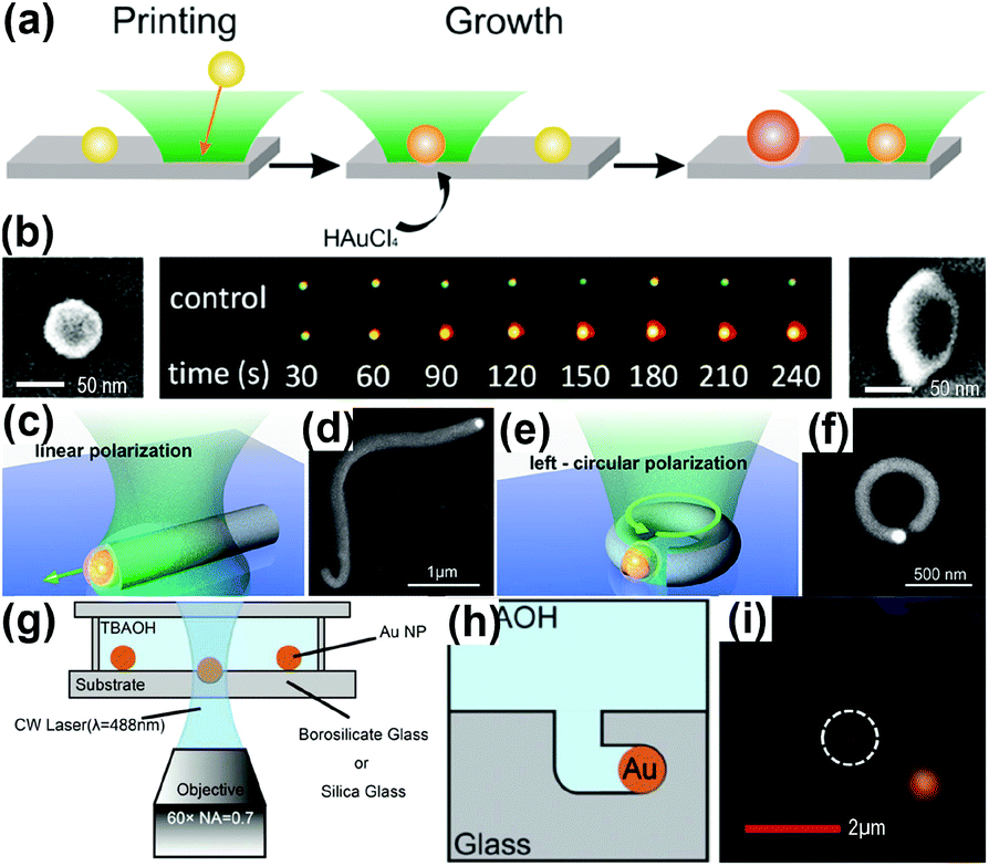 | ||
| Fig. 4 (a) Laser printed nanoparticles for light-assisted reduction of aqueous HAuCl. (b) Grown nanostructures at different laser illumination times. Reprinted with permission from ref. 49. Copyright (2016) American Chemical Society. (c) PDMS nanowire fabrication with laser heating of a single nanoparticle. (d) SEM image of the fabricated nanowire. (e) Ring-shaped PDMS pattern fabricated by heating a nanoparticle with a circularly polarized laser beam. (f) SEM image of the ring-shaped PDMS pattern. Reprinted with permission from ref. 56. Copyright (2013) American Chemical Society. (g) In situ etching-assisted laser processing with gold nanoparticles. (h) Schematic of etching a nanocavity into a glass substrate. (i) Dark-field image of the final nanocavity. Reprinted with permission from ref. 57. Copyright (2013) Royal Society of Chemistry. | ||
Fedoruk et al. demonstrated another interesting nanomanufacturing method based on the laser heating of a single gold nanoparticle as schematically shown in Fig. 4c. A single gold nanoparticle is heated by a laser beam and serves as a nano-heater to control the polymerization reaction and thermal curing of polydimethylsiloxane (PDMS) at the nanoscale.56 At the same time, the gold nanoparticle can also be moved with the laser along a predefined trajectory to form polymer nanostructures in an additive way. Fig. 4d shows a PDMS nanowire that is fabricated with a linearly polarized laser beam with this method. The laser power has to be carefully optimized to form the PDMS nanowire. The laser power has to be high enough to move the particle and start the polymerization reaction but low enough to avoid the particle getting stuck on the surface.56 Changing the polarization of the laser beam can result in different patterns. For example, a ring-shaped PDMS pattern can be formed by applying a circularly polarized laser beam as shown in Fig. 4e and f, respectively.
Osaka et al. developed an in situ etching-assisted laser processing with gold nanoparticles as schematically shown in Fig. 4g.57 The heating of a single gold nanoparticle on a glass substrate by a laser beam in an aqueous tetrabutylammonium hydroxide (TBAOH) solution allows for the etching of nanocavities deep into the glass substrate as schematically shown in Fig. 4h. Fig. 4i shows the dark-field image of the final nanocavity that is fabricated with this method. Although this method is more like a subtractive manufacturing process, other materials may be filled in the nanocavities to form new structures.
3.4 Additive nanomanufacturing based on optothermally generated surface bubble
The additive nanomanufacturing methods discussed in section 3.1–3.3 can achieve high resolutions at the single-nanoparticle level. However, the throughput is limited due to single particle manipulation. The throughput can be increased by modulating the laser beam into multiple beams by a spatial light modulator as shown in ref. 38. However, the additional optical devices for light manipulation increases the cost and complexity of the system. An optothermally generated surface bubble (OGSB) can be used to deposit multiple nanoparticles on a substrate with a simple setup for additive nanomanufacturing.An OGSB describes a micro/nano-sized bubble that is generated at a liquid–solid interface by heating the nanoparticles or solid surfaces with a laser beam as schematically shown in Fig. 5a.58 The laser can remotely control both the position and size of the OGSB. The formation of an OGSB induces a temperature gradient and a strong convective flow that can be used for a wide variety of applications.60–64Fig. 5b shows a simulated convective flow around an OGSB in a microchamber that can be used for additive nanomanufacturing.
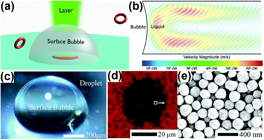 | ||
| Fig. 5 (a) An OGSB on a substrate. (b) Simulated convective flow around an OGSB in a microchamber. Reprinted with permission from ref. 58. Copyright (2017) Royal Society of Chemistry. (c) An OGSB that is generated inside a water droplet. (d) Optical image of ring-shaped close packed nanostructures fabricated on a glass substrate with an OGSB. (e) SEM image of the inner structures marked in (d) with a white box. Reprinted with permission from ref. 59. Copyright (2018) Optical Society of America. | ||
Karim et al. demonstrated the fabrication of close packed nanostructures based on an OGSB inside a liquid droplet.59Fig. 5c shows an OGSB that is generated inside a water droplet. A strong convective flow is induced by the OGSB inside the droplet. The convective flow drags the gold nanoparticles inside the droplet and deposits them at the bottom of the OGSB. Fig. 5d shows the ring-shaped close packed nanostructures fabricated on a glass substrate with this method. Fig. 5e shows the SEM image of the inner structure of the pattern marked in (d) with a white box.
Lin et al. demonstrated a “Bubble-Pen Lithography (BPL)” based on an OGSB as schematically shown in Fig. 6a.65 The working principle of the BPL is based on the generation of a micro-sized OGSB on a plasmonic substrate. The plasmonic substrate contains quasi-continuous Au nanoislands (AuNIs) with their plasmon resonance wavelength matching the heating laser wavelength. Therefore, the plasmonic substrate can enhance the photothermal effect and reduce the critical laser power for the OGSB generation. The OGSB can capture and immobilize the colloidal particles to form arbitrary particle assemblies with different resolutions and architectures with the help of the coordinated actions of Marangoni convection, surface tension, gas pressure, and substrate adhesion.65Fig. 6b shows the SEM image of a series of close packed 540 nm polystyrene beads patterned at different laser power densities. Although the authors did not test the ultimate resolution of the BPL, single-particle resolution in the range of 540 nm to 9.51 μm has been achieved by patterning single PS beads. Subsequently, the same group demonstrated the printing of quantum dots at high resolutions as schematically shown in Fig. 6c. Full-color quantum dot printing with the submicron resolution has been achieved using OGSB.66 In addition, the OGSB technique offers high throughput printing with a scanning rate of ∼10 mm s−1 and high adhesion of the quantum dots to the substrates. Fig. 6d shows a fluorescence image of Mona Lisa that is printed with red quantum dots using this method. Fig. 6e shows the detailed fluorescence image as marked with a green dashed box depicting the high-resolution patterning capability of this method. Fig. 6f shows the fluorescence lifetime imaging of the same area indicating high-density uniform patterning capability of the method. The OGSB based printing method has also been applied by other groups to print nanoparticles on a solid substrate.67–70
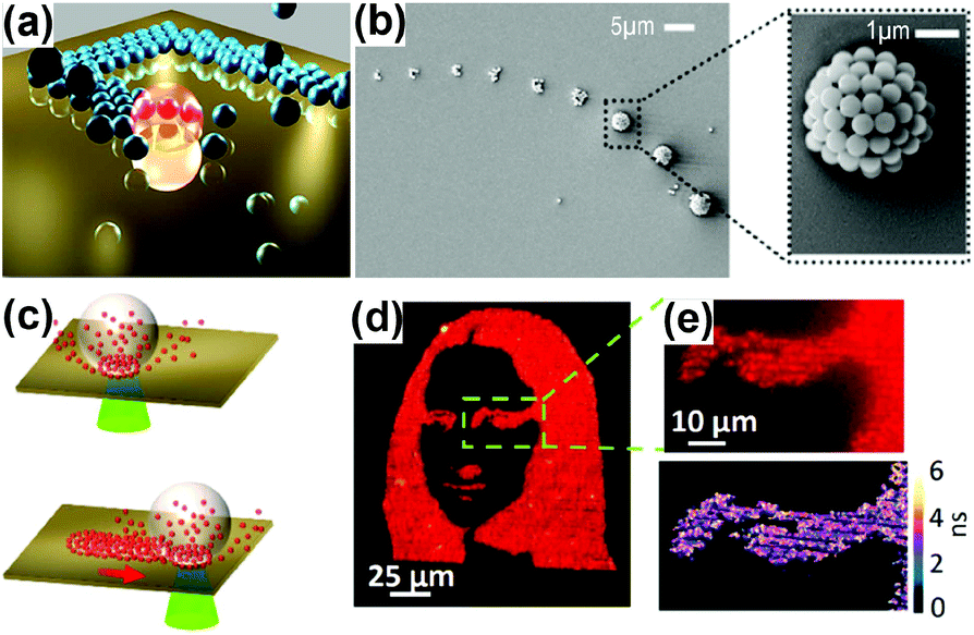 | ||
| Fig. 6 (a) Schematic of the bubble-pen lithography. (b) SEM image of a series of close packed 540 nm polystyrene beads. Reprinted with permission from ref. 65. Copyright (2016) American Chemical Society. (c) Printing of quantum dots with an OGSB. (d) Printing Mona Lisa with red quantum dots. (e) Detailed fluorescence image as marked with a green dashed box. Reprinted with permission from ref. 66. Copyright (2017) American Chemical Society. | ||
3.5 Additive nanomanufacturing based on photopolymerization
The choice of laser system plays an important role in both macro and nanoscale additive manufacturing. A continuous-wave (CW) laser is capable of conducting the additive nanomanufacturing introduced in section 3.1–3.4. Therefore, it provides a low-cost and flexible way to build the nanomanufacturing system due to the widely available CW laser systems. It is also relatively easy to apply multiple CW laser systems, for example, with different wavelengths, into a single nanomanufacturing system due to its small footprint. Another type of laser system is ultrafast laser (pulse duration of femtoseconds or picoseconds), which has been widely used in industry for applications such as laser cutting. Due to its high peak power and short-time duration, this type of laser provides the possibility for additive nanomanufacturing. One example is the additive manufacturing of polymer nanostructures through two-photon photopolymerization.71 Briefly, an ultrafast laser is focused into a polymer solution which causes the polymerization of the material at the laser focus. The laser spot can be scanned continuously in the polymer solution to form 3D nanostructures. This technology has been developed for decades and there are many review articles on this topic.72–77 Therefore, we will not elaborate much on this subject in this article. We introduce a few recent examples of additive nanomanufacturing based on this technology.Vyatskikh et al. recently showed an additive manufacturing method that allows for the fabrication of 3D metallic structures with 100 nm resolution.78Fig. 7a schematically shows the experimental setup for this approach. Hybrid organic–inorganic materials that contain Ni clusters are first synthesized to produce a metal-rich photoresist. Two-photon lithography is then applied to form the final 3D metallic structures. Fig. 7b shows the SEM images of an octet lattice that is fabricated with this method at different magnifications. The details of the 3D structure are clearly visible, which shows the effectiveness of this method for the additive manufacturing of 3D micro- and nano-architectured metals with sub-micron resolution.
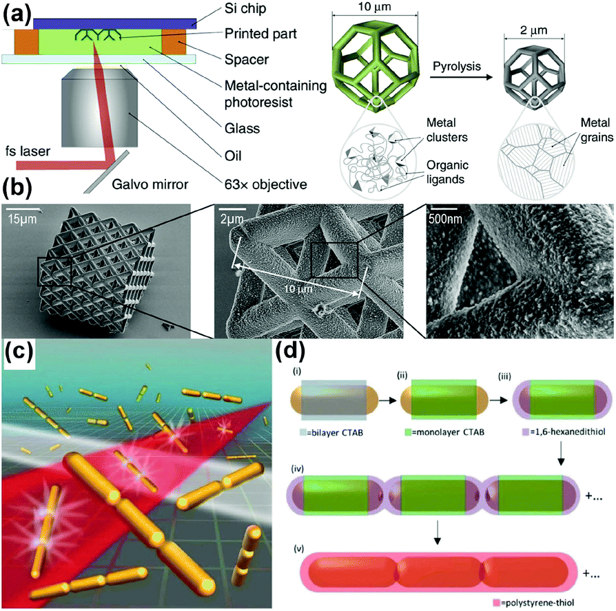 | ||
| Fig. 7 (a) Additive manufacturing of 3D nano-architected metals with 100 nm resolution. (b) SEM images of an octet lattice. Reprinted with permission from ref. 78. Copyright (2018) Springer Nature. (c) Schematic of directed assembly of nanorod antenna. (d) Procedure for directed nanorod assembly. Reprinted with permission from ref. 79. Copyright (2017) John Wiley and Sons. | ||
In addition to two-photon lithography, another example of the use of an femtosecond laser is to weld gold nanospheres or nanorods into linear chains after the individual nanoparticles have been attached by chemical linker molecules.79–81 The process used by Fontana et al. is shown schematically in Fig. 7c and the steps are shown in Fig. 7d. Gold nanorods are stabilized in a bilayer of hexadecyltrimethylammonium bromide (CTAB), then suspended in an acetonitrile![[thin space (1/6-em)]](https://www.rsc.org/images/entities/char_2009.gif) :water (8:1) solution. (1,6-Hexanedithiol) molecules link the nanorods end to end, forming a chain which grows in length as the nanorods diffuse.79 The length of the chains can be inferred from the capacitively-coupled plasmon absorption peak that appears when linking begins. The suspension is finally irradiated by a femtosecond laser to weld the nanorod dimers and trimers. Lasers can also be used to create gratings from suspensions of nanoparticles within photopolymers.82 When a photopolymer/nanoparticle suspension is holographically illuminated, monomers react to form polymers in bright areas. The unreacting nanoparticles move to low intensity areas in the interferogram, primarily due to diffusion-limited mass transport in the optically-defined gradient of polymer density.83
:water (8:1) solution. (1,6-Hexanedithiol) molecules link the nanorods end to end, forming a chain which grows in length as the nanorods diffuse.79 The length of the chains can be inferred from the capacitively-coupled plasmon absorption peak that appears when linking begins. The suspension is finally irradiated by a femtosecond laser to weld the nanorod dimers and trimers. Lasers can also be used to create gratings from suspensions of nanoparticles within photopolymers.82 When a photopolymer/nanoparticle suspension is holographically illuminated, monomers react to form polymers in bright areas. The unreacting nanoparticles move to low intensity areas in the interferogram, primarily due to diffusion-limited mass transport in the optically-defined gradient of polymer density.83
4. Additive nanomanufacturing in gaseous environment
Due to the wide availability of colloidal nanoparticles as the raw materials, conducting additive manufacturing in their native liquid environment is straightforward. However, the manufacturing methods in liquid environment discussed in section 3 also face several limitations. They are:(1) Sample contaminations: The whole substrate on which the nanostructures are fabricated is typically immersed in the colloidal nanoparticle solutions. Therefore, the nanoparticles that do not interact with the lasers would also randomly settle down on the substrate if the substrate is not properly treated. This can cause potential contamination to the fabricated nanostructures. For example, the contamination is clearly visible in Fig. 2b. This problem can be solved by tuning the surface charge of the substrate,25 however, it either adds additional procedures and cost to the system, or it's impossible to apply if the substrate is required to be in a dry environment.
(2) Low-temperature processing: The liquid environment does not allow high-temperature processing due to heat dissipation and bubble generation. The nanostructures may need local melting and sintering at high temperature to improve its properties.
Based on these considerations, additive nanomanufacturing in a dry environment is also highly desired. Therefore, we introduce several such manufacturing methods in this section.
4.1 Additive nanomanufacturing based on destructive transfer
Here, destructive laser heating means the laser either melts the materials or changes the shape of the nanostructures. Several laser-induced-forward-transfer (LIFT) methods have been developed that allow additive nano- and micro-manufacturing in air.84–88 An ultrafast pulsed laser is typically used in the LIFT method since the high peak power of the ultrafast laser allows local melting of the material and ejects it away from its native (donor) substrate towards a receiver substrate to form the final nanostructures. The LIFT technique has been used for the fabrication of metallic nanoparticles.89–94Zywietz et al. utilized laser-induced-backward-transfer (LIBT) to print silicon nanoparticles with resonant optical electric and magnetic responses.95 The LIBT process is similar to the LIFT process except the particles are ejected in a direction opposite to the direction of laser propagation.96Fig. 8a schematically shows the working principle of the LIBT technique. An ultrafast laser is focused on a silicon on insulator (SOI) wafer, which has a single crystalline silicon layer of 50 nm on a 200 nm silicon oxide substrate. The ultrafast laser causes heating and melting of the top silicon layer. The molten region forms a droplet because of the surface tension and results in an elevation of its center-of-mass. Therefore, the droplet gains an upward momentum and flies to the top receiver substrate and solidifies on contact. Silicon nanoparticles with a diameter of 160 nm have been successfully generated with this method. Fig. 8b shows SEM images of silicon nanoparticles of different diameters that are fabricated on the receiver substrate at different laser pulse energies. Larger laser pulse energies form silicon nanoparticles with larger diameters. Using this method, silicon nanoparticles with diameters in the range of 160–240 nm and larger than 400 nm have been generated.87 The final deposition position on the receiver substrate can be well controlled. The silicon nanoparticles solidified on the receiver substrate are amorphous. Interestingly, re-illuminating the amorphous silicon nanoparticle changes its crystalline state. Fig. 8c shows the dark-field microscopic image of an array of laser-printed Si nanoparticles with the nanoparticles in the white box being crystallized with additional ultrafast laser illumination.87 The crystallization process changes the optical response of the Si nanoparticle, as shown by a different color in the dark-field images. Therefore, this method not only allows for additive manufacturing of Si nanoparticles but also allows selective crystallization of single nanoparticles.
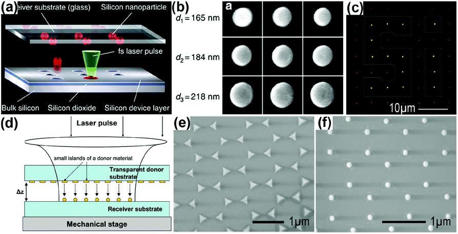 | ||
| Fig. 8 (a) Schematic of the LIBT method. (b) Silicon nanoparticles of different diameters that are fabricated on a receiver substrate with the LIBT method. (c) Optical image of an array of Si nanoparticles fabricated with the LIBT method. Reprinted with permission from ref. 95. Copyright (2014) Springer Nature. (d) Combining LIBT with conventional nanofabrication. SEM image of the triangular-shaped nanoparticle on the donor substrate (e) and the transferred nanoparticles on the receiver (f). Reprinted with permission from ref. 86. Copyright (2011) American Chemical Society. | ||
The aforementioned LIBT technique can also be used together with conventional nanofabrication for large-scale nanoparticle fabrications as schematically shown in Fig. 8d.86 Nanosphere lithography97 is used to first fabricate a hexagonal array of triangular-shaped nanoparticles with a large area on a donor substrate. A receiver substrate is placed close to the donor substrate. The triangular-shaped nanoparticles are then illuminated by a flat-top square-shaped ultrafast laser beam. The laser beam spot size is large enough to illuminate multiple nanoparticles. The triangular-shaped nanoparticles on the donor substrate melt into spherical droplets and are transferred to the receiver substrate. Fig. 8e and f shows the SEM image of the triangular-shaped nanoparticle on the donor substrate and the transferred nanoparticles on the receiver substrate,86 respectively. The period of the nanoparticles before and after the transfer is well maintained. However, the shape of the nanostructures cannot be maintained, i.e. the triangular shape changed to spherical shape due to the destructive nature of the process. In addition, LIFT has proven its ability to print few-micron sized 3D structures such as high aspect ratio pillars,98,99 multi-material out-of-plane metal microdevices,100 and complex free-standing microstructures.101
4.2 Additive nanomanufacturing based on non-destructive transfer
Recently, Alam et al. demonstrated a non-destructive nanoparticle transfer process that allows for the selective and additive transfer of nanoparticles to any substrates.102 A nanoparticle sitting on a soft substrate, such as PDMS, can be released from the substrate without damage to either the nanoparticle or the substrate, as schematically shown in Fig. 9a. Fig. 9b shows a 200 nm-diameter gold nanoparticle that is released from the substrate as highlighted with a red circle. The non-destructive release of a nanoparticle strongly depends on the type of substrate used. The same nanoparticle cannot be released from a hard substrate such as a glass substrate.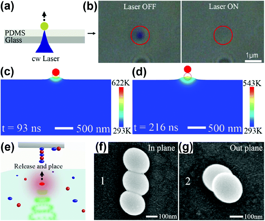 | ||
| Fig. 9 (a) A gold nanoparticle on a soft substrate. (b) Releasing a nanoparticle from a soft substrate. (c) and (d) simulation of a nanoparticle release at 93 ns and 216 ns, respectively. (e) Additively and non-destructive transfer nanoparticles between two substrate. SEM image of nanotrimer (f) and nanodimer (g). Reprinted with permission from ref. 102. Copyright (2018) American Chemical Society. | ||
When a laser beam is focused on the nanoparticle, the laser beam heats the nanoparticle and the heat transfers to the soft substrate beneath the nanoparticle. This heat transfer causes a rapid thermal expansion of the soft substrate and kicks the nanoparticle off the substrate as shown in the simulation in Fig. 9c and d. Since this transfer process depends on the elastic expansion of the soft substrate, there is no damage to the nanoparticle compared to the LIBT technique shown in Fig. 8.
Based on this non-destructive transfer technique, nanoparticles can be selectively and additively transferred to the receiver substrate to form 3D nanostructures as schematically shown in Fig. 9e. There is no limitation on the type of receiver substrate that can be used in this process. Fig. 9f and g show a nano-trimer and nano-dimer fabricated on a fiber tip with this method. Note the overlapped nanoparticles in the direction perpendicular to the surface in the nanodimer. A low-cost CW laser is used in this method and the nanoparticle can be released from the substrate with a laser power as low as 0.4 mW. Choosing the right laser wavelength can further reduce the laser power.
4.3 Additive nanomanufacturing based on laser sintering
Similar to the macroscale additive manufacturing of metal parts, where the metallic powders are either melted or sintered to form the final structures, nanostructures can also be sintered together to form the final nanostructures. Hong et al. demonstrated such a technique.103 A thin layer of silver nanoparticles are first formed on a glass substrate by spin coating to serve as the raw material, a CW laser is then focused on the nanoparticles to selectively sinter the nanoparticles. Scanning the laser beam on the substrate can form the desired nanostructures. After the laser sintering, the nanoparticles that are not sintered are washed away to develop the final pattern as schematically shown in Fig. 10a. Well-defined structures can be written on a flexible substrate as shown in Fig. 10b.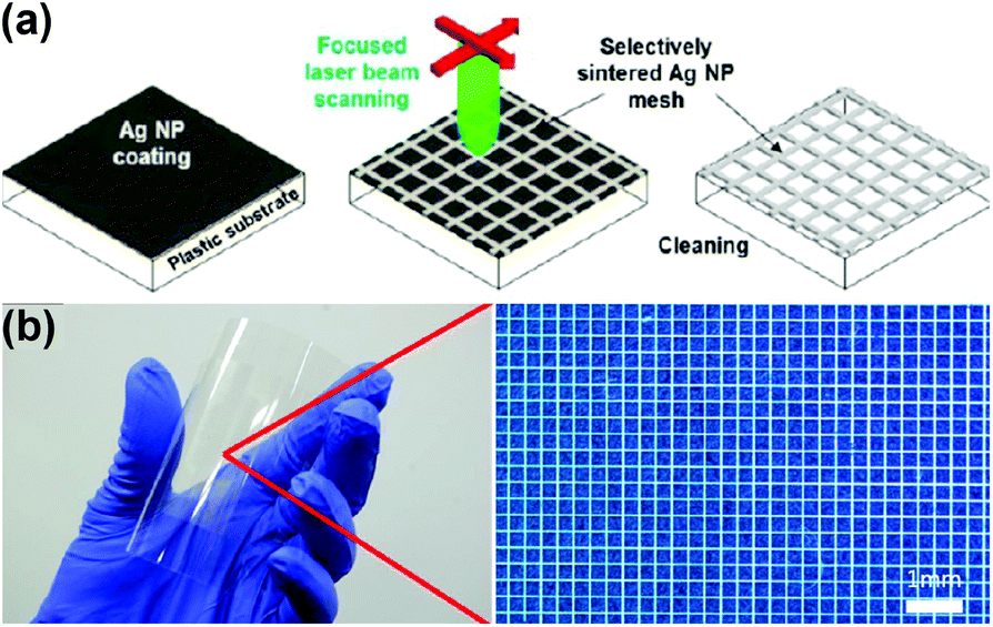 | ||
| Fig. 10 (a) Schematic of laser sintering nanoparticles. (b) Nanostructures fabricated on a flexible substrate. Reprinted with permission from ref. 103. Copyright (2013) American Chemical Society. | ||
Tong et al. applied a similar approach to write plasmonic nanostructures.104Fig. 11a schematically shows the writing process. This method depends on a local dewetting process of ultrathin gold film using a laser beam.105,106Fig. 11b shows the optical image of the ultrathin gold film with a nominal thickness of 6 nm. A green CW laser with a power of 5 W is focused in the central region of the film. Fig. 11c and d show the SEM image of the gold film without and with the laser dewetting process. As shown, the laser dewetting leads to the formation of metallic nano-islands, therefore changes the optical property of the affected region. The substrate can be scanned through the laser beam to directly write any 2D patterns. Fig. 11e shows a letter “nano” that is directly written on the thin gold film.
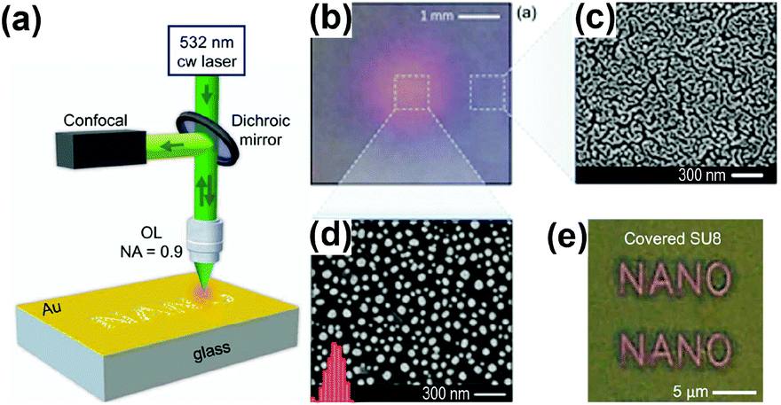 | ||
| Fig. 11 (a) Experimental setup for direct laser writing of nanostructures. (b) Optical image of an ultrathin gold film. SEM image of the gold film without (c) and with (d) laser treatment. (e) A letter “Nano” that is written on a gold film. Reprinted with permission from ref. 104. Copyright (2017) Optical Society of America. | ||
5. Applications
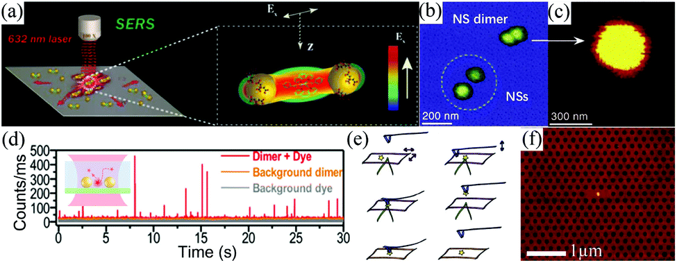
The main purpose of nanomanufacturing is to physically construct nanostructures for the realization of the promises made on the prospects of nanotechnology. The laser-based additive nanomanufacturing methods introduced in this article do not aim to replace the predominant nanomanufacturing technologies but rather seek to broaden the nanomanufacturing toolboxes that target the solution of special problems. For example, the close packed nanostructures (nano-dimers or nano-trimers) that can be manufactured by the methods introduced in this article can be used for surface enhanced Raman scattering (SERS),107–110 nonlinear optics,111–113 enhanced fluorescence emission114,115 and detection for quantum information processing.116 In addition, clusters of nanoparticles can be used as photonic metamaterials117 and for energy harvesting.118 Nanoparticle/photopolymer composites that can be manufactured by using the methods introduced in section 3.5 can be used for holographic data storage.119Fig. 12a schematically shows how the hotspot formed in the gap of a gold nano-dimer can be used for SERS. A SERS enhancement factor of 109 has been achieved in this work that is suitable for single-molecule detection.107 A gold nano-dimer can also induce a strong nonlinear effect in its gap due to the strong electric field enhancement, therefore, it can serve as a new nanoscale light source. Fig. 12b shows the atomic force microscopy (AFM) image of a gold nano-dimer (outside the dashed circle) and two separate gold nanoparticles (in the dashed circle).111Fig. 12c shows that a gold nano-dimer can generate a strong nonlinear emission but not from individual gold nanoparticles. The gold nano-dimer can also efficiently enhance the excitation and emission from a fluorescent dye as schematically shown in the inset of Fig. 12d.115Fig. 12d shows the enhanced fluorescence of Atto-655 dyes from a gold nano-dimer (red curve) compared to that outside the gold nano-dimer (grey curve). Although the nano-dimers in these examples are not manufactured by using the laser-based additive manufacturing methods, the manufacturing of similar nanostructures is possible by using, for example, the optical printing method introduced in section 3.2.
 | ||
| Fig. 12 (a) Schematic of SERS measurement on a gold nano-dimer. Reprinted with permission from ref. 107. Copyright (2017) American Chemical Society. (b) AFM image of a gold nano-dimer (outside the dashed circle) and two separate gold nanoparticles (inside the dashed circle). (c) Nonlinear emission from the gold nano-dimer. Reprinted with permission from ref. 111. Copyright (2012) Optical Society of America. (d) Enhanced fluorescence of Atto-655 dyes from a gold nano-dimer. Reprinted with permission from ref. 115. Copyright (2018) American Chemical Society. (e) Schematic of single nano-diamond manipulation with an AFM tip. (f) A single nano-diamond that is placed inside a photonic crystal membrane cavity. Reprinted with permission from ref. 120. Copyright (2011) The American Institute of Physics. | ||
In addition to the manufacturing of metallic nanoparticles for the aforementioned applications. The manufacturing and precisely positioning of other types of nanoparticles, such as quantum dots or nanodiamonds with nitrogen-vacancy (NV) color centres, is in high demand for applications in quantum information. For example, the precise position of a nanodiamond particle with a single NV centre inside a photonic device is critically important to optimize the efficient coupling between a single-photon source and a quantum device. Different methods have been developed for this purpose.120–122Fig. 12e schematically shows the manipulation of a nanodiamond with an AFM tip.120Fig. 12f shows how a single nanodiamond is successfully placed inside a photonic crystal membrane cavity. The laser-based additive nanomanufacturing methods introduced in this article can be used to achieve the same objective in a non-invasive way. For example, the optical printing method in section 3.1 and the non-destructive transfer method in section 4.2 can be potentially used to print a single nanodiamond on a photonic device either in liquid or gas environment.
6. Perspectives
Laser-based additive nanomanufacturing broadens the nanomanufacturing toolboxes for rapid prototyping and provide unique tools for applications in nanotechnology. They will also benefit from the reduced cost and increased functionality of laser systems due to the increased use of laser systems in consumer electronic industry and additive metal manufacturing in recent years. In addition, laser-based additive nanomanufacturing has the ability to work on curved and flexible substrates, therefore, it can be potentially used for the manufacturing of wearable devices under ambient conditions. The demand for new additive nanomanufacturing methods always exists in spite of the recent developments. Here, we give our insight into the following new possibilities for the future development of this promising field:Improve the uniformity of the raw nano-materials: The wide availability of nanoparticles of different sizes and materials solves the problem of material supply for laser additive nanomanufacturing. However, the light-nanoparticle interaction is very sensitive to the size and shape of the nanoparticle. Therefore, the uniformity and quality of the nanoparticles will play a critical role in uniform and consistent nanomanufacturing. The quality of the nanoparticles can be controlled by the following two ways: (1) The uniformity of the nanoparticles need to be controlled at the synthesis stage to guarantee small size distribution of the final product; (2) The nanoparticles need to be sorted and selected before going to the nanomanufacturing site.
Monitor the nanomanufacturing process in real time:
The current nanomanufacturing methods are conducted in a trial-and-error way, which means that any manufacturing errors cannot be corrected in real time. While post-processing can be applied to correct any manufacturing errors in macroscale additive manufacturing, this process is extremely challenging to apply in additive nanomanufacturing. Therefore, it is critically important to monitor the additive nanomanufacturing process in real time.
Increase throughput and scalability:
The throughput and scalability of additive nanomanufacturing are two important parameters for large-scale and affordable manufacturing of nanostructures. Most of the additive nanomanufacturing technologies introduced in this article are still in the development phase and only suitable for low-volume production. There are some commercial products for additive nanomanufacturing such as the Nanoscribe from Germany. However, the process material is still limited to polymer. Most of the additive nanomanufacturing processes are still time-consuming, especially for the manufacturing of 3D nanostructures, which face the same problem as exists in additive manufacturing at the macro scale. A combination of subtractive and additive nanomanufacturing may still be needed to achieve a better balance between manufacturing accuracy and time.
Conflicts of interest
There are no conflicts to declare.Acknowledgements
This work was supported by the National Science Foundation under award number CMMI-1761132.References
- I. Gibson, D. W. Rosen and B. Stucker, Additive Manufacturing Technologies, Springer US, Boston, MA, 2010 Search PubMed.
- D. Gu, in Laser Additive Manufacturing of High-Performance Materials, Springer Berlin Heidelberg, Berlin, Heidelberg, 2015 Search PubMed.
- A. J. Pinkerton, Opt. Laser Technol., 2016, 78, 25–32 CrossRef.
- M. Singh, H. M. Haverinen, P. Dhagat and G. E. Jabbour, Adv. Mater., 2010, 22, 673–685 CrossRef CAS PubMed.
- D. S. Engstrom, B. Porter, M. Pacios and H. Bhaskaran, J. Mater. Res., 2014, 29, 1792–1816 CrossRef CAS.
- Global nanotechnology market (by component and applications), funding & investment, patent analysis and 27 companies profile & recent developments – forecast to 2024, 2018.
- J. A. Liddle and G. M. Gallatin, ACS Nano, 2016, 10, 2995–3014 CrossRef CAS PubMed.
- B. D. Gates, Q. Xu, M. Stewart, D. Ryan, C. G. Willson and G. M. Whitesides, Chem. Rev., 2005, 105, 1171–1196 CrossRef CAS PubMed.
- J. C. Huie, Smart Mater. Struct., 2003, 12, 264–271 CrossRef CAS.
- A. Kuzuya and M. Komiyama, Nanoscale, 2010, 2, 310–322 RSC.
- K. Cooper, Micromachines, 2017, 8, 20 CrossRef.
- E. P. Koumoulos, E. Gkartzou and C. A. Charitidis, Manuf. Rev., 2017, 4, 12 Search PubMed.
- S. C. Ligon, R. Liska, J. Stampfl, M. Gurr and R. Mülhaupt, Chem. Rev., 2017, 117, 10212–10290 CrossRef CAS PubMed.
- I. Wathuthanthri, C.-H. Choi, K. Du, Y. Liu and J. Ding, Micromachines, 2017, 8, 131 CrossRef.
- J. Li, E. H. Hill, L. Lin and Y. Zheng, ACS Nano, 2019, 13, 3783–3795 CrossRef CAS PubMed.
- L. Hirt, A. Reiser, R. Spolenak and T. Zambelli, Adv. Mater., 2017, 29, 1604211 CrossRef PubMed.
- A. Piqué, R. C. Y. Auyeung, H. Kim, N. A. Charipar and S. A. Mathews, J. Phys. D: Appl. Phys., 2016, 49, 223001 CrossRef.
- H. Lee, C. H. J. Lim, M. J. Low, N. Tham, V. M. Murukeshan and Y. J. Kim, Int. J. Precis. Eng. Manuf. – Green Technol., 2017, 4, 307–322 CrossRef.
- J. A. Slotwinski, E. J. Garboczi, P. E. Stutzman, C. F. Ferraris, S. S. Watson and M. A. Peltz, J. Res. Natl. Inst. Stand. Technol., 2014, 119, 460 CrossRef CAS PubMed.
- J. Gargiulo, I. L. Violi, S. Cerrota, L. Chvátal, E. Cortés, E. M. Perassi, F. Diaz, P. Zemánek and F. D. Stefani, ACS Nano, 2017, 11, 9678–9688 CrossRef CAS PubMed.
- J. Do, M. Fedoruk, F. Jäckel and J. Feldmann, Nano Lett., 2013, 13, 4164–4168 CrossRef CAS PubMed.
- Z. Yan, R. A. Shah, G. Chado, S. K. Gray, M. Pelton and N. F. Scherer, ACS Nano, 2013, 7, 1790–1802 CrossRef CAS PubMed.
- S. Ito, H. Yoshikawa and H. Masuhara, Appl. Phys. Lett., 2002, 80, 482–484 CrossRef CAS.
- M. J. Guffey, R. L. Miller, S. K. Gray and N. F. Scherer, Nano Lett., 2011, 11, 4058–4066 CrossRef CAS PubMed.
- Y. Bao, Z. Yan and N. F. Scherer, J. Phys. Chem. C, 2014, 118, 19315–19321 CrossRef CAS.
- M. J. Guffey and N. F. Scherer, Nano Lett., 2010, 10, 4302–4308 CrossRef CAS PubMed.
- A. S. Urban, A. A. Lutich, F. D. Stefani and J. Feldmann, Nano Lett., 2010, 10, 4794–4798 CrossRef CAS PubMed.
- Z. Yan, U. Manna, W. Qin, A. Camire, P. Guyot-Sionnest and N. F. Scherer, J. Phys. Chem. Lett., 2013, 4, 2630–2636 CrossRef CAS.
- Z. Yan, J. Sweet, J. E. Jureller, M. J. Guffey, M. Pelton and N. F. Scherer, ACS Nano, 2012, 6, 8144–8155 CrossRef CAS PubMed.
- Z. Yan, S. K. Gray and N. F. Scherer, Nat. Commun., 2014, 5, 3751 CrossRef CAS PubMed.
- Z. Yan, M. Sajjan and N. F. Scherer, Phys. Rev. Lett., 2015, 114, 143901 CrossRef PubMed.
- P. Figliozzi, N. Sule, Z. Yan, Y. Bao, S. Burov, S. K. Gray, S. A. Rice, S. Vaikuntanathan and N. F. Scherer, Phys. Rev. E, 2017, 95, 022604 CrossRef PubMed.
- P. McCormack, F. Han and Z. Yan, J. Phys. Chem. Lett., 2018, 9, 545–549 CrossRef CAS PubMed.
- F. Nan, F. Han, N. F. Scherer and Z. Yan, Adv. Mater., 2018, 30, 1803238 CrossRef PubMed.
- K. Dholakia and P. Zemánek, Rev. Mod. Phys., 2010, 82, 1767–1791 CrossRef.
- M. M. Burns, J.-M. Fournier and J. A. Golovchenko, Phys. Rev. Lett., 1989, 63, 1233–1236 CrossRef CAS PubMed.
- J. E. Melzer and E. McLeod, ACS Nano, 2018, 12, 2440–2447 CrossRef CAS PubMed.
- S. Nedev, A. S. Urban, A. A. Lutich and J. Feldmann, Nano Lett., 2011, 11, 5066–5070 CrossRef CAS PubMed.
- T. Takai, H. Nakao and F. Iwata, Opt. Express, 2014, 22, 28109 CrossRef PubMed.
- J. A. Rodrigo, Sci. Rep., 2017, 7, 46506 CrossRef CAS PubMed.
- A. S. Urban, M. Fedoruk, S. Nedev, A. Lutich, T. Lohmueller and J. Feldmann, Adv. Opt. Mater., 2013, 1, 123–127 CrossRef.
- J. Gargiulo, S. Cerrota, E. Cortés, I. L. Violi and F. D. Stefani, Nano Lett., 2016, 16, 1224–1229 CrossRef CAS PubMed.
- A. G. Curto, G. Volpe, T. H. Taminiau, M. P. Kreuzer, R. Quidant and N. F. Van Hulst, Science, 2010, 329, 930–933 CrossRef CAS PubMed.
- A. N. Grigorenko, N. W. Roberts, M. R. Dickinson and Y. Zhang, Nat. Photonics, 2008, 2, 365–370 CrossRef CAS.
- H. Wang, C. S. Levin and N. J. Halas, J. Am. Chem. Soc., 2005, 127, 14992–14993 CrossRef CAS PubMed.
- N. C. Panoiu, W. E. I. Sha, D. Y. Lei and G. C. Li, J. Opt., 2018, 20, 083001 CrossRef.
- A. Grimes, D. N. Breslauer, M. Long, J. Pegan, L. P. Lee and M. Khine, Lab Chip, 2007, 8, 170–172 RSC.
- B. M. Ross, L. Y. Wu and L. P. Lee, Nano Lett., 2011, 11, 2590–2595 CrossRef CAS PubMed.
- I. L. Violi, J. Gargiulo, C. Von Bilderling, E. Cortés and F. D. Stefani, Nano Lett., 2016, 16, 6529–6533 CrossRef CAS PubMed.
- S. Linic, P. Christopher, H. Xin and A. Marimuthu, Acc. Chem. Res., 2013, 46, 1890–1899 CrossRef CAS PubMed.
- G. Baffou and R. Quidant, Chem. Soc. Rev., 2014, 43, 3898–3907 RSC.
- M. R. Langille, M. L. Personick and C. A. Mirkin, Angew. Chem., Int. Ed., 2013, 52, 13910–13940 CrossRef CAS PubMed.
- S. Linic, U. Aslam, C. Boerigter and M. Morabito, Nat. Mater., 2015, 14, 567–576 CrossRef CAS PubMed.
- Y. Xie, S. Yang, Z. Mao, P. Li, C. Zhao, Z. Cohick, P. H. Huang and T. J. Huang, ACS Nano, 2014, 8, 12175–12184 CrossRef CAS PubMed.
- M. Enders, S. Mukai, T. Uwada and S. Hashimoto, J. Phys. Chem. C, 2016, 120, 6723–6732 CrossRef CAS.
- M. Fedoruk, M. Meixner, S. Carretero-Palacios, T. Lohmüller and J. Feldmann, ACS Nano, 2013, 7, 7648–7653 CrossRef CAS PubMed.
- Y. Osaka, S. Sugano and S. Hashimoto, Nanoscale, 2016, 8, 18187–18196 RSC.
- Y. Xie and C. Zhao, Nanoscale, 2017, 9, 6622–6631 RSC.
- F. Karim, E. S. Vasquez and C. Zhao, Opt. Lett., 2018, 43, 334 CrossRef CAS PubMed.
- Q. Fan, W. Hu and A. T. Ohta, Lab Chip, 2015, 15, 581–588 RSC.
- Q. Fan, W. Hu and A. T. Ohta, Lab Chip, 2014, 14, 1572–1578 RSC.
- C. Zhao, Y. Liu, Y. Zhao, N. Fang and T. J. Huang, Nat. Commun., 2013, 4, 2305 CrossRef PubMed.
- C. Zhao, Y. Xie, Z. Mao, Y. Zhao, J. Rufo, S. Yang, F. Guo, J. D. Mai and T. J. Huang, Lab Chip, 2014, 14, 384–391 RSC.
- Y. Xie, C. Zhao, Y. Zhao, S. Li, J. Rufo, S. Yang, F. Guo and T. J. Huang, Lab Chip, 2013, 13, 1772 RSC.
- B. B. Rajeeva, Z. Mao, W. Li, E. P. Perillo, X. Peng, L. Lin, D. Akinwande, M. N. Yogeesh, A. K. Dunn and Y. Zheng, Nano Lett., 2015, 16, 701–708 Search PubMed.
- B. Bangalore Rajeeva, L. Lin, E. P. Perillo, X. Peng, W. W. Yu, A. K. Dunn and Y. Zheng, ACS Appl. Mater. Interfaces, 2017, 9, 16725–16733 CrossRef CAS PubMed.
- B. B. Rajeeva, Z. Wu, A. Briggs, P. V. Acharya, S. B. Walker, X. Peng, V. Bahadur, S. R. Bank and Y. Zheng, Adv. Opt. Mater., 2018, 6, 1701213 CrossRef.
- B. B. Rajeeva, M. A. Alabandi, L. Lin, E. P. Perillo, A. K. Dunn and Y. Zheng, J. Mater. Chem. C, 2017, 5, 5693–5699 RSC.
- Y. Zheng, H. Liu, Y. Wang, C. Zhu, S. Wang, J. Cao and S. Zhu, Lab Chip, 2011, 11, 3816 RSC.
- S. Fujii, K. Kanaizuka, S. Toyabe, K. Kobayashi, E. Muneyuki and M. Haga, Langmuir, 2011, 27, 8605–8610 CrossRef CAS PubMed.
- K. Obata, A. El-Tamer, L. Koch, U. Hinze and B. N. Chichkov, Light: Sci. Appl., 2013, 2, e116–e116 CrossRef CAS.
- F. Korte, J. Serbin, J. Koch, A. Egbert, C. Fallnich, A. Ostendorf and B. N. Chichkov, Appl. Phys. A, 2003, 77, 229–235 CAS.
- J. Serbin, A. Egbert, A. Ostendorf, B. N. Chichkov, R. Houbertz, G. Domann, J. Schulz, C. Cronauer, L. Fröhlich and M. Popall, Opt. Lett., 2003, 28, 301 CrossRef CAS PubMed.
- H. B. Sun and S. Kawata, J. Lightwave Technol., 2003, 21(3), 624 CrossRef CAS.
- J. F. Xing, M. L. Zheng and X. M. Duan, Chem. Soc. Rev., 2015, 44, 5031–5039 RSC.
- X. Zhou, Y. Hou and J. Lin, AIP Adv., 2015, 5, 030701 CrossRef.
- M. Farsari and B. N. Chichkov, Nat. Photonics, 2009, 3, 450–452 CrossRef CAS.
- X. Zhang, J. R. Greer, A. Kudo, C. M. Portela, S. Delalande and A. Vyatskikh, Nat. Commun., 2018, 9, 593 CrossRef PubMed.
- J. Fontana, R. Nita, N. Charipar, J. Naciri, K. Park, A. Dunkelberger, J. Owrutsky, A. Piqué, R. Vaia and B. Ratna, Adv. Opt. Mater., 2017, 5, 1700335 CrossRef.
- G. González-Rubio, J. González-Izquierdo, L. Bañares, G. Tardajos, A. Rivera, T. Altantzis, S. Bals, O. Peña-Rodríguez, A. Guerrero-Martínez and L. M. Liz-Marzán, Nano Lett., 2015, 15, 8282–8288 CrossRef PubMed.
- L. O. Herrmann, V. K. Valev, C. Tserkezis, J. S. Barnard, S. Kasera, O. A. Scherman, J. Aizpurua and J. J. Baumberg, Nat. Commun., 2014, 5, 4568 CrossRef CAS PubMed.
- R. A. Vaia, C. L. Dennis, L. V. Natarajan, V. P. Tondiglia, D. W. Tomlin and T. J. Bunning, Adv. Mater., 2001, 13, 1570–1574 CrossRef CAS.
- A. T. Juhl, J. D. Busbee, J. J. Koval, L. V. Natarajan, V. P. Tondiglia, R. A. Vaia, T. J. Bunning and P. V. Braun, ACS Nano, 2010, 4, 5953–5961 CrossRef CAS PubMed.
- M. Zenou and Z. Kotler, Opt. Express, 2016, 24, 1431 CrossRef CAS PubMed.
- M. Zenou, A. Sa'Ar and Z. Kotler, Small, 2015, 11, 4082–4089 CrossRef CAS PubMed.
- O. Marti, A. Koroleva, A. I. Kuznetsov, R. Kiyan, M. R. Gonçalves, A. B. Evlyukhin, M. L. Arnedillo, B. N. Chichkov and C. Reinhardt, ACS Nano, 2011, 5, 4843–4849 CrossRef PubMed.
- U. Zywietz, C. Reinhardt, A. B. Evlyukhin, T. Birr and B. N. Chichkov, Appl. Phys. A: Mater. Sci. Process., 2014, 114, 45–50 CrossRef CAS.
- A. S. Shalin, U. Zywietz, B. N. Chichkov, A. B. Evlyukhin and D. M. Zhigunov, ACS Photonics, 2018, 5, 977–983 CrossRef.
- D. A. Willis and V. Grosu, Appl. Phys. Lett., 2005, 86, 1–3 CrossRef.
- J. M. Yarbrough, C. G. Durfee, C. G. Allen, J. A. Squier, A. J. Sabbah, B. Winters and S. Bera, Appl. Opt., 2007, 46, 4650 CrossRef PubMed.
- L. Yang, C. Y. Wang, X. C. Ni, Z. J. Wang, W. Jia and L. Chai, Appl. Phys. Lett., 2006, 89, 161110 CrossRef.
- D. P. Banks, C. Grivas, J. D. Mills, R. W. Eason and I. Zergioti, Appl. Phys. Lett., 2006, 89, 193107 CrossRef.
- A. I. Kuznetsov, J. Koch and B. N. Chichkov, Opt. Express, 2009, 17, 18820 CrossRef CAS PubMed.
- C. Reinhardt, A. Seidel, R. Kiyan, A. B. Evlyukhin, B. N. Chichkov, A. I. Kuznetsov, A. Ovsianikov and W. Cheng, J. Opt. Soc. Am. B, 2009, 26, B130 CrossRef.
- U. Zywietz, A. B. Evlyukhin, C. Reinhardt and B. N. Chichkov, Nat. Commun., 2014, 5, 3402 CrossRef PubMed.
- Q. Li, D. Grojo, A. P. Alloncle, B. Chichkov and P. Delaporte, Nanophotonics, 2018, 8, 27–44 Search PubMed.
- U. C. Fischer and H. P. Zingsheim, J. Vac. Sci. Technol., 1981, 19, 881–885 CrossRef CAS.
- C. W. Visser, R. Pohl, C. Sun, G. W. Römer, B. Huis In ‘T Veld and D. Lohse, Adv. Mater., 2015, 27, 4087–4092 CrossRef CAS PubMed.
- M. Zenou, A. Sa'ar and Z. Kotler, Sci. Rep., 2015, 5, 17265 CrossRef CAS PubMed.
- J. Luo, R. Pohl, L. Qi, G. W. Römer, C. Sun, D. Lohse and C. W. Visser, Small, 2017, 13, 1602553 CrossRef PubMed.
- M. Feinaeugle, R. Pohl, T. Bor, T. Vaneker and G. W. Römer, Addit. Manuf., 2018, 24, 391–399 CrossRef CAS.
- M. S. Alam and C. Zhao, ACS Omega, 2018, 3, 1213–1219 CrossRef CAS.
- S. Hong, J. Yeo, G. Kim, D. Kim, H. Lee, J. Kwon, H. Lee, P. Lee and S. H. Ko, ACS Nano, 2013, 7, 5024–5031 CrossRef CAS PubMed.
- Q. C. Tong, M. H. Luong, J. Remmel, M. T. Do, D. T. T. Nguyen and N. D. Lai, Opt. Lett., 2017, 42, 2382 CrossRef CAS PubMed.
- C. E. Rodríguez, R. J. Peláez, C. N. Afonso, S. Riedel, P. Leiderer, D. Jimenez-Rey and A. C. Font, in Applied Surface Science, North-Holland, 2014, vol. 302, pp. 32–36 Search PubMed.
- R. Kalyanaraman, M. Khenner, R. Sachan, C. Favazza, J. Strader and H. Krishna, Nanotechnology, 2010, 21, 155601 CrossRef PubMed.
- A. Dutta and A. Chattopadhyay, J. Phys. Chem. C, 2017, 121, 18854–18861 CrossRef CAS.
- Y. Zheng, L. Rosa, T. Thai, S. H. Ng, S. Juodkazis and U. Bach, Sci. Rep., 2019, 9, 744 CrossRef PubMed.
- W. Yue, Z. Wang, J. Whittaker, F. Lopez-Royo, Y. Yang and A. V. Zayats, J. Mater. Chem. C, 2017, 5, 4075–4084 RSC.
- Y. Zheng, D. E. Gómez, U. Bach, T. Thai, S. H. Ng, L. Rosa and H. Ohshima, J. Mater. Chem. A, 2015, 3, 240–249 RSC.
- A. Slablab, L. Le Xuan, M. Zielinski, Y. de Wilde, V. Jacques, D. Chauvat and J.-F. Roch, Opt. Express, 2012, 20, 220–227 CrossRef CAS PubMed.
- Y. X. Zhang and Y. H. Wang, RSC Adv., 2017, 7, 45129 RSC.
- D. C. Marinica, A. K. Kazansky, P. Nordlander, J. Aizpurua and A. G. Borisov, Nano Lett., 2012, 12, 1333–1339 CrossRef CAS PubMed.
- A. P. Francisco, D. Botequim, D. M. F. Prazeres, V. V. Serra, S. M. B. Costa, C. A. T. Laia and P. M. R. Paulo, J. Phys. Chem. Lett., 2019, 10, 1542–1549 CrossRef CAS PubMed.
- P. M. R. Paulo, D. Botequim, A. Jóskowiak, S. Martins, D. M. F. Prazeres, P. Zijlstra and S. M. B. Costa, J. Phys. Chem. C, 2018, 122, 10971–10980 CrossRef CAS.
- S. G. Lukishova and L. J. Bissell, in Springer Series in Optical Sciences, Springer Verlag, 2019, vol. 217, pp. 103–178 Search PubMed.
- C. M. Soukoulis and M. Wegener, Nat. Photonics, 2011, 5, 523–530 CrossRef CAS.
- J. Cui, Y. Li, L. Liu, L. Chen, J. Xu, J. Ma, G. Fang, E. Zhu, H. Wu, L. Zhao, L. Wang and Y. Huang, Nano Lett., 2015, 15, 6295–6301 CrossRef CAS PubMed.
- Y. Tomita, E. Hata, K. Momose, S. Takayama, X. Liu, K. Chikama, J. Klepp, C. Pruner and M. Fally, J. Mod. Opt., 2016, 63, S1–S31 CrossRef CAS PubMed.
- A. W. Schell, G. Kewes, T. Schröder, J. Wolters, T. Aichele and O. Benson, Rev. Sci. Instrum., 2011, 82, 073709 CrossRef PubMed.
- C. Ropp, Z. Cummins, S. Nah, J. T. Fourkas, B. Shapiro and E. Waks, Nat. Commun., 2013, 4, 1447 CrossRef PubMed.
- C. Ropp, Z. Cummins, R. Probst, S. Qin, J. T. Fourkas, B. Shapiro and E. Waks, Nano Lett., 2010, 10, 4673–4679 CrossRef CAS PubMed.
| This journal is © The Royal Society of Chemistry 2019 |