
 Open Access Article
 This Open Access Article is licensed under a
 Creative Commons Attribution 3.0 Unported Licence
An ultrafast quantum thermometer from graphene quantum dots
Poonam
Sehrawat
,
Abid
and
S. S.
Islam
 *
*
Centre for Nanoscience and Nanotechnology, Jamia Millia Islamia (A Central University), New Delhi, 110025, India. E-mail: sislam@jmi.ac.in; Tel: +91 11 26987153
First published on 6th March 2019
Abstract
We report an ultra-sensitive temperature sensor derived from graphene quantum dots (GQDs) embedded in a self-standing reduced graphene oxide (RGO) film. The GQDs are obtained as a natural derivative during synthesis of GO to RGO. A fundamental study on low temperature transport mechanisms reveals the applicability of temperature zone specific ‘variable range hopping (VRH)’ conduction models, i.e. Mott-VRH, Efros–Shklovskii-VRH and activation energy supported VRH. On the basis of transport behavior and confirmed by characterization analyses, the RGO film is modeled as GQD arrays where graphitic (sp2) domains behave as QDs and oxygenated (sp3) domains between interdots act as tunneling barriers. Temperature dependent resistance and current–voltage (I–V) characteristics indicate high sensitivity where sensor resistance changes by almost six orders of magnitude as the temperature is varied between 300 and 12 K. In convection mode, the developed temperature sensor shows a temperature coefficient of resistance (TCR) of ∼−1999% K−1 in the 300–77 K temperature range, which is much higher than the TCR values reported so far. Additionally, the sensor exhibits an extremely fast response (∼0.3 s) and recovery (0.8 s) time; and such high TCR leads to ultra high resolution of ∼ μK. The sensor shows excellent repeatability with negligible drift over several cycles. These studies are crucial for modern day thermal management and sensitive cryogenic applications.
1. Introduction
Since its inception, carbon nanotechnology has opened new prospects for the synthesis and analysis of one- and two-dimensional materials wherein fundamental physics converges with device applications.1–5 One such material is graphene, whose electronic applications have been precluded by the zero bandgap at the charge neutrality point which thwarts its use in logic devices requiring frequent switching between ON/OFF states.6–17 This limitation can be overcome by modifying the band structure of graphene via lateral quantum confinement in quantum structures such as quantum dots (QDs).18–21 Since the initial studies on QD physics in the 1980s, QDs have continuously gained zealous efforts from the research community. Irrespective of the dot size, graphene quantum dots (GQDs) possess distinctive graphene structures inside the dots which endows them with some of the remarkable properties of graphene;22–26 rendering them ideal systems for observing a novel quantum phenomena and building blocks for futuristic electronic devices in sensor applications.24,26,27 Nonetheless, the handling and device fabrication pose challenges, thereby necessitating the search for alternative graphene like materials which are easy to fabricate and possess properties close to graphene. An enormous quality research study is underway to search for such materials with mass production and ease of device fabrication.The most successful routes to synthesize such materials rely on using graphite as the precursor.28–32 One such route is a chemical synthesis technique where exfoliated graphene oxide (GO) is produced in the first step and then reduced to obtain reduced graphene oxide (rGO).33–36 This technique is most suitable for economic and large scale synthesis of rGO. Despite having lowered electrical and thermal properties in comparison to pristine graphene, rGO is interesting owing to its unique properties which are an amalgamation of properties similar as well as dissimilar to those of pristine graphene.37,38 Various functional groups, such as epoxy (–O–) and hydroxyl (–OH) covalently attach on the basal plane, whereas carboxylic (–COOH) and carbonyl (–C![[double bond, length as m-dash]](https://www.rsc.org/images/entities/char_e001.gif) O) groups primarily append at the sheet edges.18 Besides, sp3 → sp2 carbon transformation in rGO is not hundred percent complete and causes considerable defects or disorders which can trap charge carriers.39 Additionally, the conductivity of an rGO film can be controlled by varying the film thickness which in turn depends upon the synthesis parameters (e.g., ultrasonication, reduction time, etc.).3 Thus, rGO has gained immense scientific interest due to – (a) large scale production; (b) modifiable properties which can be controlled by tuning the sp2 to sp3 carbon ratio; and (c) a possibility of further modifying the rGO structure (and hence its properties) via functionalization with different nanoparticles as well as organic molecules.40 This behavior is attributed to the presence of significant disorders on the rGO films. Thus, a comprehensive study needs to be undertaken to analyze the effect of synthesis conditions on all these parameters.
O) groups primarily append at the sheet edges.18 Besides, sp3 → sp2 carbon transformation in rGO is not hundred percent complete and causes considerable defects or disorders which can trap charge carriers.39 Additionally, the conductivity of an rGO film can be controlled by varying the film thickness which in turn depends upon the synthesis parameters (e.g., ultrasonication, reduction time, etc.).3 Thus, rGO has gained immense scientific interest due to – (a) large scale production; (b) modifiable properties which can be controlled by tuning the sp2 to sp3 carbon ratio; and (c) a possibility of further modifying the rGO structure (and hence its properties) via functionalization with different nanoparticles as well as organic molecules.40 This behavior is attributed to the presence of significant disorders on the rGO films. Thus, a comprehensive study needs to be undertaken to analyze the effect of synthesis conditions on all these parameters.
Interestingly, much of the initial work on graphene based devices, in general, has been on field effect transistors (FETs). Development of a smart temperature sensor from graphene is a relatively new area of research.41–43 Although a substantial amount of work has been done on the carrier transport mechanism in graphene,17,38,44–48 hardly any studies are available on the development of temperature sensors either from graphene or GQD arrays, exploiting their carrier transport properties. In the case of carrier transport in graphene or 2D materials, the current flow is controlled by scattering events;49–52 whereas in GQDs, the current will exist only if carriers overcome the Coulomb blockade potential.53,54 The temperature dependent differential change in resistance/current in the circuit is the key factor for the development of a highly sensitive temperature sensor. Two major sensing parameters, i.e. temperature coefficient of resistance (TCR) and thermal hysteresis (HTh) are very crucial since both of them control the quantification of heat sensing characteristic parameters including sensitivity, response- and recovery-time, resolution and repeatability. Interestingly, not many reports are present on GQD based temperature sensors and no concrete report is presented so far.
In this article, we present the rich transport phenomena observed in the rGO/alumina self-standing film where the resistance can be tuned over more than six orders of magnitude vis-à-vis its room temperature value. The rGO film has been converted into nanometre sized graphitic zones (termed as graphene quantum dots or GQDs) caged within insulating zones (barrier). The GQDs, distributed in disordered arrays, demonstrate elevated temperature (T ∼ 300 K) activated hopping, and direct quantum tunneling depending on the spatial interdot separation and operating temperature. The temperature sensor fabricated from this film shows TCR values of −7946.5% K−1 and −1999.8% K−1 in the temperature ranges of 300–12 K and 300–77 K, respectively. Such a high TCR leads to the achievement of ultra-resolution of ∼ μK, and a response-and recovery-time of 0.3 s and 0.8 s respectively in convection mode. Cycling tests conducted at 77 K show negligible drift over several cycles. Additionally, this work presents an example of reversible metal–insulator transition in a solid-state system implying the prospects of producing novel solid-state materials, based on GQDs, wherein the electronic band structure of the material can be ‘tailored’ by adjusting the electronic wave function overlap between neighboring dots.
2. Materials and methods
2.1. Materials synthesis
Transformation of graphite to graphene oxide (GO) via a chemical conversion technique has surfaced as a convenient method to produce graphene like monolayers with considerable yield.51,52,55 Modified Hummers’ method based oxidative treatment of natural graphite flakes was performed to prepare graphite oxide.56 Unlike pristine graphite, GO is highly oxidized having oxygenated epoxide bonds on the basal plane, whereas carbonyl and carboxyl groups are present at the sheet edges. Single- to few-layered GO sheets were obtained by exfoliation of graphite oxide in DI using a bath sonicator (90 minutes). The presence of oxygen moieties makes GO sheets readily soluble in DI, resulting in stable aqueous suspensions of nearly 1 nm thick sheets under mild sonication conditions.57 GO was then washed and dried under ambient conditions. Chemical reduction of the GO powder was carried out by dissolving 500 mg GO in 500 mL DI followed by 1 h of sonication. To this mixture, 50 μL hydrazine hydrate was mixed and the solution was refluxed at a constant temperature (98 °C) for varying time periods (1, 2, 3, and 5 h). At this point, the color changed from yellowish brown to black, indicating the conversion of GO to rGO. The RGO powder was obtained by suction filtering and washing the suspension with DI followed by subsequent drying at 60 °C in an inert (N2) ambient atmosphere for 10 h.51,52 The reduction process removes epoxy groups from the basal plane resulting in regeneration of C–C bonds.55To understand the mechanism of the above reactions, we can consider a graphene lattice,58 where three out of four valence electrons from each C atom are covalently bound to three neighboring C atoms. These bound electrons are called σ-electrons and the corresponding bonds are termed as σ-bonds or C–C bonds. The fourth electron from each C atom (termed as π-electron) is free to move around the graphene layer, and thus acts as a charge carrier. In the hexagonal lattice of graphene, these π-electrons occupy six individual corners of the first Brillouin zone (also called the Dirac points).58 During oxidation, each oxygen (O) atom uses two π-electrons from two C-atoms and meets its octet requirements, thereby forming epoxy bonds. However, neither σ-electrons nor σ-bonds are altered to fulfill octet requirements because the bond energy of C–O (358 kJ mol−1) is much lower vis-à-vis C–C (473 kJ mol−1) in graphene.58–60 Four types of oxygenated functional groups exist in GO, these are61
(a) Epoxide (–O–): attached to the basal plane.
(b) Hydroxyl (–OH): along the basal plane.
(c) Carbonyl (–CO): distributed along the edges.
(d) Carboxyl (–COOH): attached to the edges.
Out of these, epoxide and hydroxyl groups dominate the total oxygen functionalities glued to GO sheets.38 During reduction by a chemical route or thermal treatment, the C–O bonds break, thereby again freeing the π-electrons. In this way, graphene oxide recovers its pristine state by clearing the oxygen debris created during the oxidation process. Further, there was no apparent involvement of either σ-electrons or σ-bonds (or C–C bonds) unless aggressive oxidation/reduction is pursued. Thus, the graphene lattice is usually intact and no considerable point defects are introduced. Additionally, carbonyl and carboxyl groups cannot be removed without destroying the graphene basal plane.62
GO to rGO transformation leads to the creation of graphene quantum dots (GQDs) within the rGO maze and their sizes vary from a few nm to 100 nm depending on the degree of conversion from sp3 to sp2 bonding. The graphene region (sp2 bonding) shows semi-metallic behavior whereas the remaining sp3 region is insulating. Physical properties of rGO are considerably affected by the sp2/sp3 hybridized carbon ratio, and the presence of different functional moieties. Therefore, the electrical conduction process through the rGO sheet becomes complex and it shows the Coulomb blockade phenomena for charge transport, specifically at low temperatures.23,55,63,64 Growth of QDs in the rGO film have been studied by several groups,23,63–66 where the degree of reduction during the synthesis process and atomic scale features are studied and characterized with various microscopic and spectroscopic techniques.
2.2. Materials characterization
O bond (287.3 eV, grey curve); and (4) the C(O)O or OC–OH bond (289.2 eV ± 0.4 eV, green curve). Fig. 1(b–e) show the C1's spectra of rGO, where gradual attenuation and disappearance of some oxygenated groups are apparent. The C–C peak represents the sp2 carbon fraction, while the oxygenated functional moieties present at the basal plane of the sheets and sheet edges signify sp3-hybridized carbon fraction.38,67,69,70 The sp2 carbon fraction is obtained from the ratio of the integrated peak areas of the C–C peak to the total area under the C1's spectrum:40
 | ||
| Fig. 1 XPS spectra of the rGO sample for (a) 0 h (GO), (b) 1 h, (c) 2 h, (d) 3 h, and (e) 5 h of reduction treatment. (f) Shows the variation of sp2 carbon as a function of reduction time. The inset to (f) is a structural model of GO at various steps of the reduction process. Here, dark areas indicate sp2 carbon domains, and light grey areas are sp3 carbons consisting of oxygen groups (depicted as small dots). Reproduced with permission from ref. 18. | ||
The results in Fig. 1(f) indicate that sp2 carbon fraction (or reduction efficiency) of the rGO sheet increases from ∼57% for GO (0 h) to ∼80% for rGO treated for 5 h.
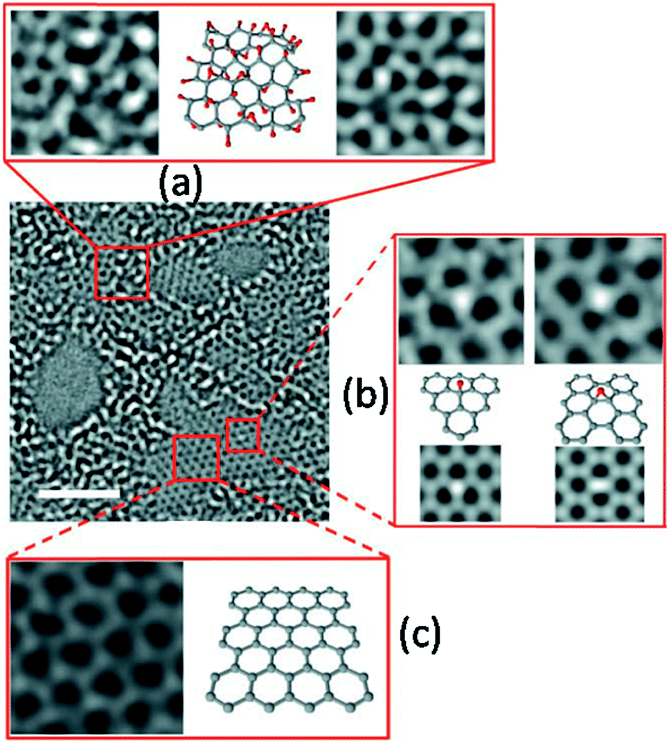 | ||
| Fig. 2 Aberration-corrected TEM images of a monolayer GO on a 2 nm scale. (a) Leftmost image shows the 1 nm2 enlarged oxidized region in GO, the middle image is its suggested atomic structure where grey dots represent carbon atoms and red dots are oxygen atoms, and the rightmost image is the average of a simulated TEM micrograph of the suggested structure and a simulated TEM image of a second structure with changed positions of oxygen containing groups. (b) Enlarged image of the white spot in the graphitic region. This spot moved along the graphitic region, but stayed stationary for three frames (6 s) at a hydroxyl position (left side of expansion (b)) and for seven frames (14 s) at a (1, 2) epoxy position (right side of expansion (b)). The ball-and-stick figures below the microscopy images show the proposed atomic structures for these functional groups. The simulated TEM image for the proposed structure is in agreement with the observed TEM structure. Enlarged image in (c) displays a 1 nm2 graphitic section from the exit plane wave reconstruction of a focal series of GO and the atomic structure of this region. Reproduced with permission from ref. 72. | ||
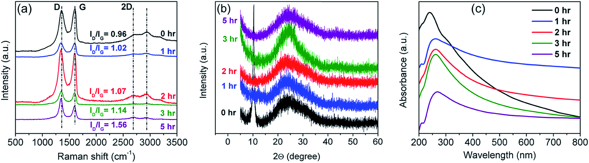 | ||
| Fig. 3 (a) Raman spectra, (b) XRD patterns, and (c) UV-Vis spectra of the prepared rGO sample as a function of reduction time. | ||
2.3. Temperature sensor fabrication
The rGO (treated for 5 h) prepared in Section 2.1 was used for temperature sensor fabrication. A self-standing film of the rGO/alumina nanocomposite was prepared via sol–gel processing where 0.6 wt% rGO powder was mechanically added to 99.4 wt% alumina sol as elaborated in ref. 77–79. The temperature sensor was fabricated from this film by slicing pieces of 10 mm × 10 mm size from it and depositing silver electrodes at the two end terminals of the sample.3. Results and discussion
3.1. Charge transport mechanism
Current–voltage (I–V) characteristics of the fabricated sensor were studied in a four probe helium cryostat (Oxford Instruments) where cryo-pumping maintained the base pressure at ∼10−7 torr throughout the experiment. Proper care was taken to prevent stray radiation and condensation of residual moisture on the rGO film mounted inside the cryostat. The system is designed for low current measurements of the order of picoampere (pA). Current and voltage sweeps were programmed via LabView programme.I–V measurements conducted in the 300–12 K temperature range are plotted in Fig. 4(a). The recorded plots are highly symmetric and non-linear below 100 K. Sensor breakdown was not observed even at the bias voltages of ±20 V. Low temperature (≤100 K) I–V plots indicate current suppression below a certain threshold voltage, VTh.This current suppression can be attributed to the Coulomb blockade phenomenon as extensively explained in ref. 40, 80–84. VTh is found to be both temperature as well as bias dependent. As evident from Fig. 4(b), the threshold voltage decreases linearly with temperature up to 94 K and it becomes negative after extrapolation beyond 94 K.80–84 The negative VTh has been attributed to the Coulomb blockade phenomenon by several authors.80–84
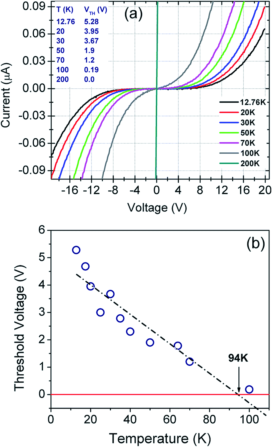 | ||
| Fig. 4 (a) Temperature dependent I–V plots of the sensor in the bias range from −20 V to +20 V. (b) Threshold voltage (VTh) as a function of temperature. | ||
The resistance versus temperature and its semi-logarithmic plot is shown in Fig. 5. There is an anomalous jump in resistance of more than six orders of magnitude as the temperature is reduced from 273 K to 12 K. The relatively high change in conductivity vis-à-vis graphene is due to the presence of residual functional groups (i.e., sp3 bonding) and disorders in rGO.38,80–89 Several distinct regions are clearly observed (as demonstrated in the TEM image), similar to disordered semiconductors.80,85
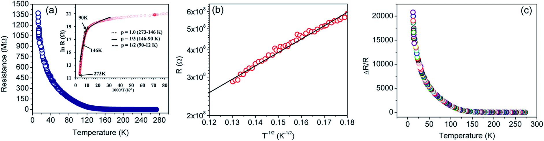 | ||
| Fig. 5 (a) Resistance (R) versus temperature (T) plot for the rGO sample in the 273–12 K temperature range. Inset shows R (in log scale) versus 1/T plot. The dotted, solid and dashed lines are fits to eqn (1) of the experimental data of (a), using p = 1, 1/3, and 1/2, respectively. (b) R versus T−1/2 plot in the semi-log scale. The solid black line represents linear fit for a T−1/2 behavior of the experimental points (red circles). (c) Normalized change in resistance as a function of temperature. | ||
On the basis of XPS and Raman data, the rGO sheet may be considered as a two-dimensional (2D) array of GQDs where graphitic domains behave as QDs while oxygenated domains act as tunnel barriers. The temperature dependent charge-transport mechanism in rGO is generally supported by three independent theories, i.e. Mott variable range hopping (Mott-VRH),38,86 Efros–Shklovskii variable range hopping (ES-VRH),55,87,88 and thermal activation52,89 supported VRH – also known as Arrhenius type; and these are highly temperature zone specific. While looking into the theoretical aspects, there is a serious disagreement on the temperature scaling factor even for an identical temperature range; and this is because the results were obtained with different sample geometries, reduction processes, reduction temperatures and the reduction routes.88 Therefore, the transport mechanism in GQD arrays in rGO is an important subject in the field of graphene based electronics.
The temperature dependent resistance behavior shown in Fig. 5 probably originates from the characteristic of the strongly localized region of VRH. Mott38,88 theory relies on three specific criteria – (1) localized defect states are created near the Fermi level during GO to rGO conversion; and carrier transport occurs via hopping from one state to another by taking energy either from a phonon or directly from an externally applied electric field; (2) at low temperatures, the nearest neighbor hopping will not dominate; rather the hopping electron will always try to achieve the lowest activation energy (ΔE) and shortest hopping distance. Generally, these two conditions are not fulfilled simultaneously; and there exists an optimum hopping distance rhop, corresponding to maximum hopping probability; and (3) there is no Coulomb interaction between the localized states. The standard Mott-VRH relation is:40
 | (1) |
Efros–Shklovskii (ES) proposed that defect states are localized around the Fermi level, transport occurs via hopping and there is Coulomb interaction among carriers. This idea results in R scaling as (T)−1/2.40,90
 | (2) |
The scaling factor p turns out to be −1 in the case of Arrhenius theory of activation energy induced hopping and the relation is:80
 | (3) |
Best linear fits were obtained for  in the temperature range of 90–12 K pointing toward ES-VRH as a plausible charge-transport phenomenon in rGO layers consisting of GQD arrays. The other fitted values are
  in the 146–90 K temperature range where Mott-VRH is applicable. The temperature range of 273–146 K comes under Arrhenius type of conduction via activation energy where p = 1 is the best fit. The temperature range of 100–80 K may be a mixed zone where ES-VRH and Mott-VRH both coexist.
The ES-VRH suggests strong localization of wave functions in GQDs. Its further analysis allows the calculation of localization length ξ by plotting R against T−1/2 in a semi-log scale (Fig. 5(b)).91–93 From the slope of the curve, T0 = 4170 K is obtained. T0 is related to ξ through:40,87
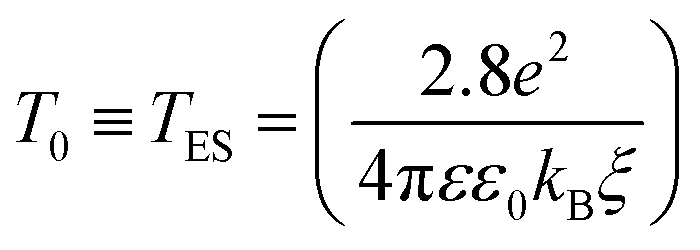 | (4) |
3.2. Temperature sensing studies
The temperature sensing measurement was conducted in a two probe system fitted with a liquid nitrogen closed cycle system (Fig. 6). The heating/cooling induced electrical response was monitored in the temperature range of 300–77 K and was recorded using a Keithley 4200 SCS. A Linkam T95-PE system temperature controller was employed to maintain the targeted temperature. Below 77 K, measurements could not be conducted due to the limitation of the liquid nitrogen cryostat. | ||
| Fig. 6 (a) Photographic image of the developed rGO/alumina composite self-standing film. Schematics of the (b) experimental setup employed to measure the temperature dependent sensor response, and (c) directions of the electric field and heat flux. | ||
3.3. TCR and hysteresis analysis
In a temperature sensor, we encounter two interdependent physical properties of the material, i.e. thermal (κ) and electrical (σ) conductivities; and both are responsible for heat and carrier transportation. Their interdependence determines the temperature coefficient of resistance (TCR) and thermal hysteresis loss (HTh), thereby playing an important role in efficient operation of the sensing device. A large TCR is critical for improved sensitivity, resolution, drift, and response- and recovery time.52,77,78The TCR is directly calculated from the sensing measurements in non-contact, i.e. convection mode (Fig. 7), where the sensor was shifted from room temperature and exposed to the targeted temperature. The TCR values are tabulated in Table 1 for each temperature range along with the response- and recovery-time. The maximum TCR observed is −1999.8% K−1 in the temperature range of 300–77 K with a unique slope and ultra-fast response time of ∼0.3 s. Such an unprecedented increase of TCR indicates the superior performance of the sensor in terms of sensitivity and resolution. The constant slope has an added advantage that the device may not need further calibration. Further, the baseline shift is practically nil in all the cycles, therefore, thermal hysteresis does not come under purview.
 | ||
| Fig. 7 (a) Sensor operation at a specific temperature by exposing (or removing) it to a target temperature from room temperature, and (b) the corresponding response and recovery time of the sensor. | ||
| Initial temperature (K) | Final temperature (K) | TCR (−% K−1) | Response time (s) | Recovery time (s) |
|---|---|---|---|---|
| 296 | 373 | 0.98 | 3.96 | 6.01 |
| 296 | 348 | 1.20 | 3.99 | 5.70 |
| 296 | 333 | 1.26 | 3.92 | 5.69 |
| 296 | 318 | 1.24 | 1.99 | 5.42 |
| 300 | 218 | 36.6 | 12.0 | 1.52 |
| 300 | 188 | 94.3 | 11.4 | 1.48 |
| 300 | 178 | 155.5 | 10.4 | 1.40 |
| 300 | 168 | 218.7 | 9.00 | 1.30 |
| 300 | 163 | 267.6 | 8.30 | 1.20 |
| 300 | 153 | 369.8 | 6.40 | 1.00 |
| 300 | 129 | 907.2 | 4.90 | 0.95 |
| 300 | 117 | 1753.7 | 2.90 | 0.99 |
| 300 | 77 | 1999.8 | 0.30 | 0.80 |
In addition to this, we have also carried out temperature sensing tests at high temperatures, i.e. in the 296–373 K temperature range. The test results are incorporated in Table 1 and plotted in Fig. 8(a). The corresponding response and recovery time are shown in Fig. 8(b).
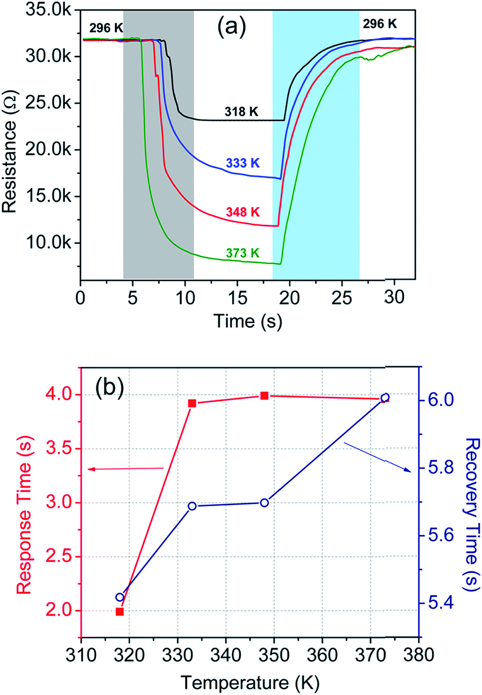 | ||
| Fig. 8 (a) Sensor response at different temperatures in the 296–373 K temperature range, and (b) response and recovery time of the sensor at the corresponding temperatures. | ||
3.4. Cycling test at low temperature
Fig. 9 shows the cycling test of the sensor in the temperature range of 300–77 K. Excellent repeatability with a unique profile is observed in all the cycles. The response- and recovery time are found to be of the order of few seconds and shown in Table 1. Interestingly, envelope shaped oscillations appear in the sensor response. The reason for such oscillations is not clearly understood, but can be attributed to the current fluctuations when the device achieves extremely high resistance (∼GΩ) and intermittent current suppression takes place.94 This experiment could not be extended beyond 77 K owing to the limitation of our sensing setup which is based on closed cycle liquid nitrogen.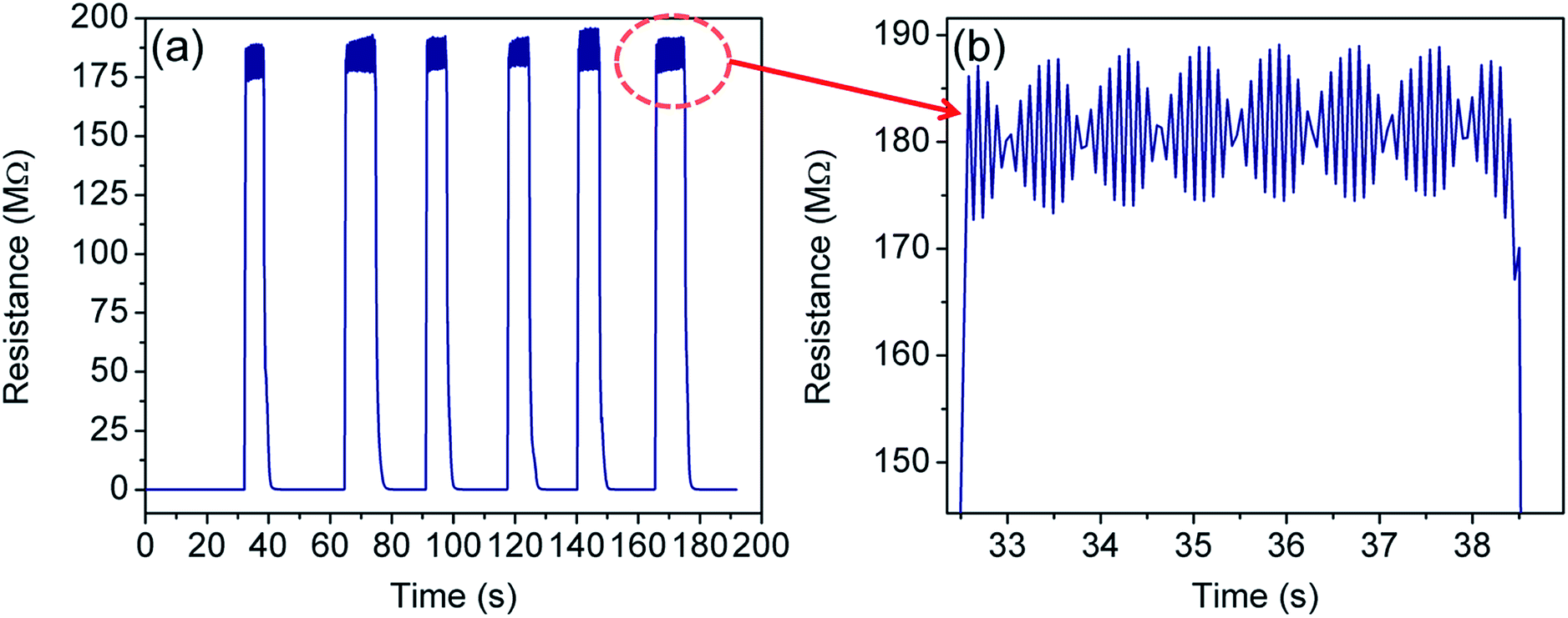 | ||
| Fig. 9 (a) Sensor response when the sensor is frequently dipped into liquid nitrogen for short time durations, and (b) zoomed in image of the highlighted spot in (a) showing the formation of the oscillatory pattern (in the form of an envelope) at 77 K. | ||
Interestingly, the envelope pattern resembles – (1) the superposition of the signal and carrier frequency as seen in the case of amplitude modulation in communication engineering,95 (2) the de-Haas van Alphen effect under a magnetic field,96 and (3) the superposition of a group of waves having slightly different wavelengths from each other while propagating in a medium.97 Notably, the oscillations of the envelope as well as the wave pattern within the envelope were found periodic and their frequency of oscillation is 0.61 Hz and 10 Hz respectively. In the present case, the first two cases can be discarded as there is neither a high frequency (carrier wave) source nor any magnetic field applied to the sensing system. Therefore, the last one is most probable and needs further explanation.
We propose these to be the Coulomb blockade effects in terms of tunneling strength between coupled dots. The type of coupling between QDs influences the character of the electronic states and the nature of transport through the QD array. Theoretical prediction supports phase transition for tunneling in coupled GQD arrays.98–100 The ratio of interdot separation (D) and size (L) of the QD clearly measures the coupling strength between dots. While assuming L as a constant, the coupling strength may be classified in terms of D as follows
(1) For a large D, there is no interaction among QDs and the CB of individual QDs is preserved, i.e. the number of peaks is equal to the number of energy levels within a single QD. Each peak signifies the addition of electrons to the array, one to each GQD at the same time.
(2) When D is the intermediate, the CB of individual QDs is lifted and a combined CB effect across the QD array materializes.
(3) For low D, original energy levels split in subbands; these will cross each other and the CB will be completely diluted.
Due to the formation of high density QDs, there is a possibility to have charge particle interactions between the dots and it may be supported from the second point (2) mentioned above. As a result, the de-Broglie waves of the electrons may superimpose and the oscillatory envelope function may evolve from individual to collective electronic states in a dense QD assembly.99–104
In our case, D and L parameters are taken as average values because GQDs were self-created as a consequence of the chemical reduction process. Therefore, the Coulomb force due to interdot coupling is affected by the dilution effect arising from high temperature as well as high bias voltage. At a high bias voltage, the charging energy becomes negligible and the envelope disappears. Similarly, when the temperature is very high, the Coulomb force between GQDs gets diluted resulting in the disappearance of the envelope.
3.5. Resolution test
Fig. 10 shows the change in resistance at different temperature step sizes from 273–77 K. The temperature step size (ΔT) is micro-tuned to reach the targeted temperature and the corresponding change in resistance (ΔR) was measured accordingly. At a target temperature of 77 K, ΔR was found to be ∼MΩ for ΔT = 0.1 K (after extrapolation of the curve). For a gross simplification, if we assume the measurable signal strength to be within the 10–100 Ω range, then the signal obtained for ΔT = 0.1 K will correspond to a measurable temperature resolution of ∼μK. Measurements beyond 0.1 K change could not be carried out in our system due to the limitation of the temperature controller employed. As seen from Fig. 10(b), the change in resistance corresponding to a change in temperature by 0.1 K is around 3.4 kΩ indicating high resolution of the developed device. | ||
| Fig. 10 (a) Resolution test done in non-contact mode. The yellow shaded region shows the extrapolated points for the change in resistance for a 0.1 K change in temperature. (b) Shows sensor response at 193 K for a 0.1 K step change in temperature. | ||
The performance of the fabricated sensor is found to be much better than most of the existing sensors reported so far.105–117 A comparison is presented in Table 2 to assess its performance vis-à-vis some of the recently reported temperature sensors.
| Materials | Temperature range (K) | TCR (% K−1) | Other parameters | References |
|---|---|---|---|---|
| Copper oxide (CuO): pure CuO press-tablets CuO–Si-adhesive | 298–353 | −5.2 | — | 105 |
| −4.0 | ||||
| Co-doped ZnO based thermistor | 293–553 | −20 | — | 106 |
| Graphene nanowalls (GNWs)@polydimethylsiloxane (PDMS) substrate | 308–318 | +21.40 | Response time = 1.6 s | 107 |
| Recovery time = 8.52 s | ||||
| Resolution = 0.1 K | ||||
| Reduced graphene oxide (RGO) nanosheets/elastomeric polyurethane (PU) composite | 303–353 |

|
Resolution = 0.2 K | 108 |
Cyclability = 10![[thin space (1/6-em)]](https://www.rsc.org/images/entities/char_2009.gif) 000 cycles 000 cycles |
||||
| Ag@polyimide based thermistor | 293–333 | +0.22 | Thermal hysteresis = <5% | 109 |
| Pentacene/Ag NPs based organic field-effect transistor | 293–373 | ΔR/R = 20.4 | Resolution = 0.4 K | 110 |
| Monolayer graphene based pyroelectric bolometer | ΔT = 0.2 K | 900 | Resolution = 15 μK | 111 |
| RGO decorated ZnO nanosheets | 233–353 | −0.205 | — | 112 |
| CNT@PET substrate | 233–373 | −0.4 | Response time = 0.3 s | 113 |
| Recovery time = 4 s | ||||
| Multi-walled carbon nanotubes (MWCNTs)/alumina composite | 303–373 | −0.96 | Response time = 40 s | 114 |
| Recovery time = 185 s | ||||
| Thermal hysteresis = 0.62% | ||||
| Poly(3,4-ethylenedioxythiophene):poly(styrenesulfonate) (PEDOT:PSS)@paper substrate based thermistor | 263–298 | −3 | — | 115 |
| Copper oxide nanowires (CuO NWs) grown on a glass substrate | 293–453 | ∼1.3 | — | 116 |
| Vanadium pentoxide thin films | 319–343 | ∼−4 | — | 117 |
| RGO/alumina composite | 300–77 | −1999.8 | Response time = 0.3 s | Present work |
| Recovery time = 0.8 s | ||||
| 296–373 | −0.98 | Response time = 3.96 s | ||
| Recovery time = 6.01 s |
4. Conclusion
GQD arrays, developed in the rGO film during the chemical reduction process from GO to rGO, act as a maze where poly-dispersed graphene QDs are semimetallic, and the interdot space is an insulating zone, called the tunnel barrier. Coulomb blockade and charge carrier tunneling through the tunnel barrier is largely associated with metal and semiconductor quantum dots. The carrier transport is explained using suitable VRH models where the ESH–VRH model fits well in the low temperature regime. The average QD size or the electron localization length was found to be ∼3.2 nm. This has allowed us to translate these phenomena into making a real device, i.e. an ultra-sensitive low temperature thermometer with very high resolution along with the fastest response and recovery. TCR and thermal hysteresis loss are considered as the main characteristic parameters that control the quality of most of the sensor parameters and the sensor ratings. Surprisingly, both of them appeared to be exceptional in making the sensing device ultra-sensitive both in cryogenic and high temperature measurement. The cycling test revealed that the sensor is stable for over 50 cycles with an ultra-fast response time. A highly sensitive temperature sensor is in great demand for cryogenic temperature measurements in industry, healthcare, and R&D laboratories; and the proposed sensor may fulfill the need of these sectors. An interesting fact is that the sensors are cheap and reproducible. Identical rGO sheets were developed and tested successfully to justify our claim. Further, no such comprehensive report is available in the literature on the development of graphene quantum dot based temperature sensor to date.Conflicts of interest
There are no conflicts to declare.Acknowledgements
The authors gratefully acknowledge the support of Prof. Shakeel Ahmad (Aligarh Muslim University, Aligarh) for carrying out the cryo-temperature measurements and Dr K. Asokan (Inter University Accelerator Centre, New Delhi) for cross-checking the experimental results and fruitful discussion. The authors are thankful to Dr A. K. Kapoor (Solid State Physics Laboratory, New Delhi) for his generous support for XPS measurements.References
- P. L. McEuen, Nature, 1998, 393, 15 CrossRef CAS.
- Y. Xia, P. Yang, Y. Sun, Y. Wu, B. Mayers, B. Gates, Y. Yin, F. Kim and H. Yan, Adv. Mater., 2003, 15, 353–389 CrossRef CAS.
- G. Eda and M. Chhowalla, Adv. Mater., 2010, 22, 2392–2415 CrossRef CAS PubMed.
- S. Z. Butler, S. M. Hollen, L. Cao, Y. Cui, J. A. Gupta, H. R. Gutiérrez, T. F. Heinz, S. S. Hong, J. Huang, A. F. Ismach and E. Johnston-Halperin, ACS Nano, 2013, 7, 2898–2926 CrossRef CAS PubMed.
- D. Jariwala, V. K. Sangwan, L. J. Lauhon, T. J. Marks and M. C. Hersam, ACS Nano, 2014, 8, 1102–1120 CrossRef CAS PubMed.
- K. S. Novoselov, A. K. Geim, S. V. Morozov, D. Jiang, Y. Zhang, S. V. Dubonos, I. V. Grigorieva and A. A. Firsov, Science, 2004, 306, 666–669 CrossRef CAS PubMed.
- C. Berger, Z. Song, T. Li, X. Li, A. Y. Ogbazghi, R. Feng, Z. Dai, A. N. Marchenkov, E. H. Conrad, P. N. First and W. A. De Heer, J. Phys. Chem. B, 2004, 108, 19912–19916 CrossRef CAS.
- Y. Zhang, Y. W. Tan, H. L. Stormer and P. Kim, Nature, 2005, 438, 201 CrossRef CAS PubMed.
- F. Schedin, A. K. Geim, S. V. Morozov, E. W. Hill, P. Blake, M. I. Katsnelson and K. S. Novoselov, Nat. Mater., 2007, 6, 652 CrossRef CAS PubMed.
- A. A. Balandin, S. Ghosh, W. Bao, I. Calizo, D. Teweldebrhan, F. Miao and C. N. Lau, Nano Lett., 2008, 8, 902–907 CrossRef CAS PubMed.
- R. R. Nair, P. Blake, A. N. Grigorenko, K. S. Novoselov, T. J. Booth, T. Stauber, N. M. Peres and A. K. Geim, Science, 2008, 320, 1308 CrossRef CAS PubMed.
- K. I. Bolotin, K. J. Sikes, Z. Jiang, M. Klima, G. Fudenberg, J. Hone, P. KiM and H. L. Stormer, Solid State Commun., 2008, 146, 351–355 CrossRef CAS.
- A. C. Neto, F. Guinea, N. M. Peres, K. S. Novoselov and A. K. Geim, Rev. Mod. Phys., 2009, 81, 109 CrossRef.
- D. C. Elias, R. R. Nair, T. M. G. Mohiuddin, S. V. Morozov, P. Blake, M. P. Halsall, A. C. Ferrari, D. W. Boukhvalov, M. I. Katsnelson, A. K. Geim and K. S. Novoselov, Science, 2009, 323, 610–613 CrossRef CAS PubMed.
- S. H. Cheng, K. Zou, F. Okino, H. R. Gutierrez, A. Gupta, N. Shen, P. C. Eklund, J. O. Sofo and J. Zhu, Phys. Rev. B: Condens. Matter Mater. Phys., 2010, 81, 205435 CrossRef.
- Z. Wei, D. Wang, S. Kim, S. Y. Kim, Y. Hu, M. K. Yakes, A. R. Laracuente, Z. Dai, S. R. Marder, C. Berger and W. P. King, Science, 2010, 328, 1373–1376 CrossRef CAS PubMed.
- S. D. Sarma, S. Adam, E. H. Hwang and E. Rossi, Rev. Mod. Phys., 2011, 83, 407 CrossRef.
- C. Mattevi, G. Eda, S. Agnoli, S. Miller, K. A. Mkhoyan, O. Celik, D. Mastrogiovanni, G. Granozzi, E. Garfunkel and M. Chhowalla, Adv. Funct. Mater., 2009, 19, 2577–2583 CrossRef CAS.
- J. Haskins, A. Kınacı, C. Sevik, H. Sevinçli, G. Cuniberti and T. Ç.nd, ACS Nano, 2011, 5, 3779–3787 CrossRef CAS PubMed.
- R. Balog, B. Jørgensen, L. Nilsson, M. Andersen, E. Rienks, M. Bianchi, M. Fanetti, E. Lægsgaard, A. Baraldi, S. Lizzit and Z. Sljivancanin, Nat. Mater., 2010, 9, 315 CrossRef CAS PubMed.
- D. V. V. D. Haberer, D. V. Vyalikh, S. Taioli, B. Dora, M. Farjam, J. Fink, D. Marchenko, T. Pichler, K. Ziegler, S. Simonucci and M. S. Dresselhaus, Nano Lett., 2010, 10, 3360–3366 CrossRef CAS PubMed.
- M. Bacon, S. J. Bradley and T. Nann, Part. Part. Syst. Charact., 2014, 31, 415–428 CrossRef CAS.
- L. A. Ponomarenko, F. Schedin, M. I. Katsnelson, R. Yang, E. W. Hill, K. S. Novoselov and A. K. Geim, Science, 2008, 320, 356–358 CrossRef CAS PubMed.
- J. Shen, Y. Zhu, X. Yang and C. Li, Chem. Commun., 2012, 48, 3686–3699 RSC.
- D. Pan, J. Zhang, Z. Li and M. Wu, Adv. Mater., 2010, 22, 734–738 CrossRef CAS PubMed.
- S. I. Ahn, J. Jung, Y. Kim, Y. Lee, K. Kim, S. E. Lee, S. Kim and K. K. Choi, Sci. Rep., 2016, 6, 38830 CrossRef CAS PubMed.
- D. Kong, L. T. Le, Y. Li, J. L. Zunino and W. Lee, Langmuir, 2012, 28, 13467–13472 CrossRef CAS PubMed.
- S. Stankovich, D. A. Dikin, R. D. Piner, K. A. Kohlhaas, A. Kleinhammes, Y. Jia, Y. Wu, S. T. Nguyen and R. S. Ruoff, Carbon, 2007, 45, 1558–1565 CrossRef CAS.
- Z. J. Fan, W. Kai, J. Yan, T. Wei, L. J. Zhi, J. Feng, Y. M. Ren, L. P. Song and F. Wei, ACS Nano, 2010, 5, 191–198 CrossRef PubMed.
- J. Wang, K. K. Manga, Q. Bao and K. P. Loh, J. Am. Chem. Soc., 2011, 133, 8888–8891 CrossRef CAS PubMed.
- P. Song, X. Zhang, M. Sun, X. Cui and Y. Lin, RSC Adv., 2012, 2, 1168–1173 RSC.
- Y. Si and E. T. Samulski, Nano Lett., 2008, 8, 1679–1682 CrossRef CAS PubMed.
- A. Bagri, C. Mattevi, M. Acik, Y. J. Chabal, M. Chhowalla and V. B. Shenoy, Nat. Chem., 2010, 2, 581 CrossRef CAS PubMed.
- C. Botas, P. Álvarez, P. Blanco, M. Granda, C. Blanco, R. Santamaría, L. J. Romasanta, R. Verdejo, M. A. López-Manchado and R. Menéndez, Carbon, 2013, 65, 156–164 CrossRef CAS.
- O. C. Compton and S. T. Nguyen, Small, 2010, 6, 711–723 CrossRef CAS PubMed.
- V. López, R. S. Sundaram, C. Gómez-Navarro, D. Olea, M. Burghard, J. Gómez-Herrero, F. Zamora and K. Kern, Adv. Mater., 2009, 21, 4683–4686 CrossRef.
- D. C. Marcano, D. V. Kosynkin, J. M. Berlin, A. Sinitskii, Z. Sun, A. Slesarev, L. B. Alemany, W. Lu and J. M. Tour, ACS Nano, 2010, 4, 4806–4814 CrossRef CAS PubMed.
- C. Gómez-Navarro, R. T. Weitz, A. M. Bittner, M. Scolari, A. Mews, M. Burghard and K. Kern, Nano Lett., 2007, 7, 3499–3503 CrossRef PubMed.
- K. A. Mkhoyan, A. W. Contryman, J. Silcox, D. A. Stewart, G. Eda, C. Mattevi, S. Miller and M. Chhowalla, Nano Lett., 2009, 9, 1058–1063 CrossRef CAS PubMed.
- D. Joung, Electronic Transport Investigation of Chemically Derived Reduced Graphene Oxide Sheets, PhD thesis, University of Central Florida, 2012 Search PubMed.
- H. Wang, Y. Wang, X. Cao, M. Feng and G. Lan, J. Raman Spectrosc., 2009, 40, 1791–1796 CrossRef CAS.
- J. W. Jiang, H. S. Park and T. Rabczuk, Nanoscale, 2014, 6, 3618–3625 RSC.
- F. Hao, D. Fang and Z. Xu, Appl. Phys. Lett., 2011, 99, 041901 CrossRef.
- E. H. Hwang, S. Adam and S. D. Sarma, Phys. Rev. Lett., 2007, 98, 186806 CrossRef CAS PubMed.
- X. Du, I. Skachko, A. Barker and E. Y. Andrei, Nat. Nanotechnol., 2008, 3, 491 CrossRef CAS PubMed.
- K. I. Bolotin, K. J. Sikes, J. Hone, H. L. Stormer and P. Kim, Phys. Rev. Lett., 2008, 101, 096802 CrossRef CAS PubMed.
- W. Zhu, V. Perebeinos, M. Freitag and P. Avouris, Phys. Rev. B, 2009, 80, 235402 CrossRef.
- S. Tanabe, Y. Sekine, H. Kageshima, M. Nagase and H. Hibino, Phys. Rev. B: Condens. Matter Mater. Phys., 2011, 84, 115458 CrossRef.
- A. A. Balandin, Nat. Mater., 2011, 10, 569 CrossRef CAS PubMed.
- H. Schmidt, S. Wang, L. Chu, M. Toh, R. Kumar, W. Zhao, A. H. Castro Neto, J. Martin, S. Adam, B. Özyilmaz and G. Eda, Nano Lett., 2014, 14, 1909–1913 CrossRef CAS PubMed.
- Abid, P. Sehrawat, S. S. Islam, P. Mishra and S. Ahmad, Sci. Rep., 2018, 8, 3537 CrossRef CAS PubMed.
- P. Sehrawat, Abid, S. S. Islam and P. Mishra, Sens. Actuators, B, 2018, 258, 424–435 CrossRef CAS.
- N. F. Mott, Metal-Insulator Transitions, Taylor & Francis, London, 1990 Search PubMed.
- K. C. Beverly, J. L. Sample, J. F. Sampaio, F. Remacle, J. R. Heath and R. D. Levine, Proc. Natl. Acad. Sci. U. S. A., 2002, 99, 6456–6459 CrossRef CAS PubMed.
- V. Singh, D. Joung, L. Zhai, S. Das, S. I. Khondaker and S. Seal, Prog. Mater. Sci., 2011, 56, 1178–1271 CrossRef CAS.
- S. Park, J. An, R. D. Piner, I. Jung, D. Yang, A. Velamakanni, S. T. Nguyen and R. S. Ruoff, Chem. Mater., 2008, 20, 6592–6594 CrossRef CAS.
- S. Stankovich, R. D. Piner, X. Chen, N. Wu, S. T. Nguyen and R. S. Ruoff, J. Mater. Chem., 2006, 16, 155–158 RSC.
- Y. Mulyana, M. Uenuma, Y. Ishikawa and Y. Uraoka, J. Phys. Chem. C, 2014, 118, 27372–27381 CrossRef CAS.
- G. Glockler, J. Phys. Chem., 1958, 62, 1049–1054 CrossRef CAS.
- D. W. Brenner, O. A. Shenderova, J. A. Harrison, S. J. Stuart, B. Ni and S. B. Sinnott, J. Phys.: Condens. Matter, 2002, 14, 783 CrossRef CAS.
- X. Gao, J. Jang and S. Nagase, J. Phys. Chem. C, 2009, 114, 832–842 CrossRef.
- K. P. Loh, Q. Bao, G. Eda and M. Chhowalla, Nat. Chem., 2010, 2, 1015 CrossRef CAS PubMed.
- C. Stampfer, J. Güttinger, F. Molitor, D. Graf, T. Ihn and K. Ensslin, Appl. Phys. Lett., 2008, 92, 012102 CrossRef.
- C. Stampfer, E. Schurtenberger, F. Molitor, J. Guttinger, T. Ihn and K. Ensslin, Nano Lett., 2008, 8, 2378–2383 CrossRef CAS PubMed.
- J. Wurm, A. Rycerz, I. Adagideli, M. Wimmer, K. Richter and H. U. Baranger, Phys. Rev. Lett., 2009, 102, 056806 CrossRef PubMed.
- J. H. Bardarson, M. Titov and P. W. Brouwer, Phys. Rev. Lett., 2009, 102, 226803 CrossRef CAS PubMed.
- H. C. Schniepp, J. L. Li, M. J. McAllister, H. Sai, M. Herrera-Alonso, D. H. Adamson, R. K. Prud'homme, R. Car, D. A. Saville and I. A. Aksay, J. Phys. Chem. B, 2006, 110, 8535–8539 CrossRef CAS PubMed.
- D. A. Dikin, S. Stankovich, E. J. Zimney, R. D. Piner, G. H. Dommett, G. Evmenenko, S. T. Nguyen and R. S. Ruoff, Nature, 2007, 448, 457 CrossRef CAS PubMed.
- A. Lerf, H. He, M. Forster and J. Klinowski, J. Phys. Chem. B, 1998, 102, 4477–4482 CrossRef CAS.
- I. Jung, D. A. Dikin, R. D. Piner and R. S. Ruoff, Nano Lett., 2008, 8, 4283–4287 CrossRef CAS PubMed.
- C. T. Chien, S. S. Li, W. J. Lai, Y. C. Yeh, H. A. Chen, I. S. Chen, L. C. Chen, K. H. Chen, T. Nemoto, S. Isoda and M. Chen, Angew. Chem., Int. Ed., 2012, 51, 6662–6666 CrossRef CAS PubMed.
- K. Erickson, R. Erni, Z. Lee, N. Alem, W. Gannett and A. Zettl, Adv. Mater., 2010, 22, 4467–4472 CrossRef CAS PubMed.
- M. A. Pimenta, G. Dresselhaus, M. S. Dresselhaus, L. G. Cancado, A. Jorio and R. Saito, Phys. Chem. Chem. Phys., 2007, 9, 1276–1290 RSC.
- Z. Ni, Y. Wang, T. Yu and Z. Shen, Nano Res., 2008, 1, 273–291 CrossRef CAS.
- A. C. Ferrari and J. Robertson, Phys. Rev. B: Condens. Matter Mater. Phys., 2000, 61, 14095 CrossRef CAS.
- F. Tuinstra and J. L. Koenig, J. Chem. Phys., 1970, 53, 1126–1130 CrossRef CAS.
- P. Sehrawat, P. Mishra and S. S. Islam, Mater. Sci. Semicond. Process., 2015, 31, 116–123 CrossRef CAS.
- P. Sehrawat and S. S. Islam, Mater. Res. Bull., 2016, 80, 72–79 CrossRef CAS.
- Abid, P. Sehrawat, S. S. Islam, P. Gulati, M. Talib, P. Mishra and M. Khanuja, Sens. Actuators, A, 2018, 269, 62–69 CrossRef CAS.
- H. E. Romero and M. Drndic, Phys. Rev. Lett., 2005, 95, 156801 CrossRef PubMed.
- A. S. Cordan, Y. Leroy, A. Goltzené, A. Pépin, C. Vieu, M. Mejias and H. Launois, J. Appl. Phys., 2000, 87, 345–352 CrossRef CAS.
- M. G. Ancona, W. Kruppa, R. W. Rendell, A. W. Snow, D. Park and J. B. Boos, Phys. Rev. B: Condens. Matter Mater. Phys., 2001, 64, 033408 CrossRef.
- R. Parthasarathy, X. M. Lin, K. Elteto, T. F. Rosenbaum and H. M. Jaeger, Phys. Rev. Lett., 2004, 92, 076801 CrossRef PubMed.
- A. Bezryadin, R. M. Westervelt and M. Tinkham, Appl. Phys. Lett., 1999, 74, 2699–2701 CrossRef CAS.
- N. F. Mott and E. A. Davis, Electronic processes in non-crystalline materials, OUP Oxford, 2012 Search PubMed.
- A. B. Kaiser, C. Gómez-Navarro, R. S. Sundaram, M. Burghard and K. Kern, Nano Lett., 2009, 9, 1787–1792 CrossRef CAS PubMed.
- D. Joung and S. I. Khondaker, Phys. Rev. B: Condens. Matter Mater. Phys., 2012, 86, 235423 CrossRef.
- M. Park, S. J. Hong, K. H. Kim, H. Kang, M. Lee, D. H. Jeong, Y. W. Park and B. H. Kim, Appl. Phys. Lett., 2017, 111, 173103 CrossRef.
- S. Wang, P. J. Chia, L. L. Chua, L. H. Zhao, R. Q. Png, S. Sivaramakrishnan, M. Zhou, R. G. S. Goh, R. H. Friend, A. T. S. Wee and P. K. H. Ho, Adv. Mater., 2008, 20, 3440–3446 CrossRef CAS.
- A. A. Middleton and N. S. Wingreen, Phys. Rev. Lett., 1993, 71, 3198 CrossRef CAS PubMed.
- A. L. Efros and B. I. Shklovskii, J. Phys. C: Solid State Phys., 1975, 8, L49 CrossRef CAS.
- J. Zhang and B. I. Shklovskii, Phys. Rev. B: Condens. Matter Mater. Phys., 2004, 70, 115317 CrossRef.
- A. L. Efros and M. Pollak, Electron-electron interactions in disordered systems, Elsevier, 2012 Search PubMed.
- N. W. Ashcroft and N. D. Mermin, Solid state physicsHolt, rinehart and winston, New York, 1976, 2005 Google Scholar, p. 403 Search PubMed.
- G. Kennedy and B. Davis, Electronic communication systems, Tata McGraw-Hill Publishing Co. Ltd., New Delhi, 1985, vol. 20, p. 21 Search PubMed.
- N. W. Ashcroft and N. D. Mermin, Solid state physics, Holt, rinehart and winston, New York, 1976, vol. 2005, Google Scholar, p. 403 Search PubMed.
- J. S. Blakemore, Solid State Physics, Cambridge University Press, 2nd edn, 1985 Search PubMed.
- C. A. Stafford and S. D. Sarma, Phys. Rev. Lett., 1994, 72, 3590 CrossRef CAS PubMed.
- C. P. Collier, R. J. Saykally, J. J. Shiang, S. E. Henrichs and J. R. Heath, Science, 1997, 277, 1978–1981 CrossRef CAS.
- Q. Ma, T. Tu, L. Wang, C. Zhou, Z. R. Lin, M. Xiao and G. P. Guo, Mod. Phys. Lett. B, 2013, 27, 1350008 CrossRef.
- J. J. Shiang, J. R. Heath, C. P. Collier and R. J. Saykally, J. Phys. Chem. B, 1998, 102, 3425–3430 CrossRef CAS.
- S. Henrichs, C. P. Collier, R. J. Saykally, Y. R. Shen and J. R. Heath, J. Am. Chem. Soc., 2000, 122, 4077–4083 CrossRef CAS.
- M. V. Artemyev, A. I. Bibik, L. I. Gurinovich, S. V. Gaponenko and U. Woggon, Phys. Rev. B: Condens. Matter Mater. Phys., 1999, 60, 1504 CrossRef CAS.
- M. V. Artemyev, U. Woggon, H. Jaschinski, L. I. Gurinovich and S. V. Gaponenko, J. Phys. Chem. B, 2000, 104, 11617–11621 CrossRef CAS.
- S. B. Khan, M. T. S. Chani, K. S. Karimov, A. M. Asiri, M. Bashir and R. Tariq, Talanta, 2014, 120, 443–449 CrossRef CAS PubMed.
- X. F. Zhou, H. Zhang, H. Yan, C. L. He, M. H. Lu and R. Y. Hao, Appl. Phys. A: Mater. Sci. Process., 2014, 114, 809–812 CrossRef CAS.
- J. Yang, D. Wei, L. Tang, X. Song, W. Luo, J. Chu, T. Gao, H. Shi and C. Du, RSC Adv., 2015, 5, 25609–25615 CAS.
- T. Q. Trung, S. Ramasundaram, B. U. Hwang and N. E. Lee, Adv. Mater., 2016, 28, 502–509 CrossRef CAS PubMed.
- M. D. Dankoco, G. Y. Tesfay, E. Bènevent and M. Bendahan, Mater. Sci. Eng., B, 2016, 205, 1–5 CrossRef CAS.
- X. Ren, K. Pei, B. Peng, Z. Zhang, Z. Wang, X. Wang and P. K. Chan, Adv. Mater., 2016, 28, 4832–4838 CrossRef CAS PubMed.
- U. Sassi, R. Parret, S. Nanot, M. Bruna, S. Borini, D. De Fazio, Z. Zhao, E. Lidorikis, F. H. L. Koppens, A. C. Ferrari and A. Colli, Nat. Commun., 2017, 8, 14311 CAS.
- V. Gaddam, RGO decorated ZnO nanosheets for Temperature Sensor Applications, 2017 Search PubMed.
- V. S. Turkani, D. Maddipatla, B. B. Narakathu, B. J. Bazuin and M. Z. Atashbar, Sens. Actuators, A, 2018, 279, 1–9 CAS.
- P. Sehrawat, Abid, S. S. Islam, P. Mishra and M. Khanuja, Mater. Res. Bull., 2018, 99, 1–9 CrossRef CAS.
- J. Maslik, H. Andersson, V. Forsberg, M. Engholm, R. Zhang and H. Olin, J. Instrum., 2018, 13, C12010 CrossRef.
- A. A. Aljubouri, A. D. Faisal and W. K. Khalef, Mater. Sci.-Pol., 2018, 36, 460–468 CAS.
- S. V. Grayli, G. W. Leach and B. Bahreyni, Sens. Actuators, A, 2018, 279, 630–637 CrossRef CAS.
| This journal is © The Royal Society of Chemistry 2019 |