
 Open Access Article
 This Open Access Article is licensed under a Creative Commons Attribution-Non Commercial 3.0 Unported Licence
Enhanced charge separation in g-C3N4–BiOI heterostructures for visible light driven photoelectrochemical water splitting†
Kazi M.
Alam‡
a,
Pawan
Kumar‡
 a,
Piyush
Kar
a,
Ujwal K.
Thakur
a,
Sheng
Zeng
a,
Kai
Cui
b and
Karthik
Shankar
*a
a,
Piyush
Kar
a,
Ujwal K.
Thakur
a,
Sheng
Zeng
a,
Kai
Cui
b and
Karthik
Shankar
*a
aDepartment of Electrical & Computer Engineering, University of Alberta, Edmonton, AB T6G 1H9, Canada. E-mail: kshankar@ualberta.ca; Tel: +1 780-492-1354
bNanotechnology Research Centre, National Research Council of Canada, Edmonton, Canada T6G 2M9
First published on 7th January 2019
Abstract
Heterojunctions of the low bandgap semiconductor bismuth oxyiodide (BiOI) with bulk multilayered graphitic carbon nitride (g-C3N4) and few layered graphitic carbon nitride sheets (g-C3N4-S) are synthesized and investigated as an active photoanode material for sunlight driven water splitting. HR-TEM and elemental mapping reveals formation of a unique heterostructure between BiOI platelets and the carbon nitride (g-C3N4 and g-C3N4-S) network that consisted of dendritic BiOI nanoplates surrounded by g-C3N4 sheets. The presence of BiOI in g-C3N4-S/BiOI and g-C3N4-S/BiOI nanocomposites extends the visible light absorption profile from 500 nm up to 650 nm. Due to excellent charge separation in g-C3N4/BiOI and g-C3N4-S/BiOI, evident from quenching of the carbon nitride photoluminescence (PL) and a decrease in the PL lifetime, a significant increase in photoelectrochemical performance is observed for both types of g-C3N4–BiOI heterojunctions. In comparison to heterojunctions of bulk g-C3N4 with BiOI, the nanocomposite consisting of few layered sheets of g-C3N4 and BiOI exhibits higher photocurrent density due to lower recombination in few layered sheets. A synergistic trap passivation and charge separation is found to occur in the g-C3N4-S/BiOI nanocomposite heterostructure which results in a higher photocurrent and a lower charge transfer resistance.
1. Introduction
The search for renewable and environment-friendly alternative energy sources is among the most focused research activities of the current scientific community. Solar energy is abundant, renewable and sustainable. Hydrogen molecules have the potential to act as a portable chemical fuel where harvested solar energy can be stored. The potential of photoelectrochemical water splitting for high capacity storage of solar energy was recognized from an early era.1,2 In a typical photoelectrochemical cell involving an n-type semiconductor active layer, electron–hole pairs are generated in the semiconductor photoanode upon illumination of light. Under an applied bias, photogenerated electrons travel through the semiconductor anode and the external circuit to the counter electrode where they participate in water reduction to evolve hydrogen while photogenerated holes are directly transferred from the photoanode to the electrolyte to perform water oxidation to evolve oxygen. The valence band maximum of the semiconductor photoanode needs to be below the oxidation potential of the oxygen evolution reaction (H2O + 2h+ → 2H+ + 1/2O2) for efficient hole transfer to the electrolyte. An ideal semiconductor photoanode needs to possess many desirable attributes such as broadband optical absorption (i.e. a low bandgap), a high absorption coefficient for visible photons (to generate a large number of electron–hole pairs per unit volume), a high charge separation efficiency, a low charge transfer resistance, plentiful availability of active sites, good chemical and photocorrosion stability, cost-effectiveness etc. Traditional photocatalysts such as TiO2 and composite TiO2 nanomaterials have been extensively studied in the past.3,4 However, wide bandgaps significantly hinder the visible light absorption capacity of these materials, a fact that has promoted an intense search for finding new earth-abundant, photocatalytic semiconductor systems.Metal-free, low cost and robust graphitic carbon nitride (g-C3N4) has proved to be a highly promising potential photocatalyst for producing hydrogen by water splitting since it has a moderate bandgap (2.6 eV) and suitable band-edge positions. This material is abundant in nature, environment-friendly, and has good thermal, photochemical and chemical stability.5–7 This semiconductor consists of tri-s-triazine units positioned in a two-dimensional graphitic polymer structure.8 The photocatalytic performance of this material suffers from poor absorption of red and near-infrared photons (due to bandgap value as well as low oscillator strength), a small specific surface area and a rapid carrier recombination rate.6,9 Many attempts have been made in order to enhance the photocatalytic performance of graphitic carbon nitride by synthesizing nanosheets, post-calcination, engineering crystal lattice structure, designing nanostructures and forming heterojunctions with other suitable semiconductors.6,9–15 In bulk carbon nitride, inter-sheets hydrogen bonding, and multilayered sheets stacking promotes localized interlayer charge recombination processes which significantly reduce the availability of charge carriers.16 Bulk carbon nitride is composed of stacked carbon nitride sheets randomly interconnected via hydrogen bonding between terminal NH2 and primary or secondary N's (NH2/C–N![[double bond, length as m-dash]](https://www.rsc.org/images/entities/char_e001.gif) C).17 The small effective surface area of stacked sheets and localized charge recombination in hydrogen bonded sheets lead to poor intralayer carrier transport. Bulk carbon nitride can be transformed into few layered or monolayer sheets which increase available surface area and reduce inter-sheets hydrogen bonding which improve charge transport and minimize charge recombination process.18,19 Various solvent exfoliation approaches have been used for the transformation of bulk carbon nitride into sheets, however the use of such chemicals is undesirable due to tedious workup, hazardous nature and energy intensive ultrasonication or thermal heating.20,21 The addition of N rich precursors such as NH4Cl which liberates NH3 and HCl gases at elevated temperature facilitates the transformation of bulk sheets into few layered sheets is appealing due to the avoidance of hazardous chemicals involved in chemical exfoliation. During thermal annealing of dicyandiamide and NH4Cl mixture at high temperature the released NH3 and HCl from breakdown of NH4Cl which blew dicyandiamide derived polymers into numerous large bubbles, which behaves as gas templates and yielded few layered g-C3N4 nanosheets.11 Earth abundant bismuth oxyhalides (BiOX, X = Cl, Br, I) constitute another recently discovered ternary compound semiconductor family that has gathered significant attention due to the small bandgaps of compounds in this family (1.7–1.9 eV) and a layered tetragonal crystal structure.22–24 In this family, BiOI has been reported to exhibit the highest photocatalytic activities due to its narrow bandgap.25
C).17 The small effective surface area of stacked sheets and localized charge recombination in hydrogen bonded sheets lead to poor intralayer carrier transport. Bulk carbon nitride can be transformed into few layered or monolayer sheets which increase available surface area and reduce inter-sheets hydrogen bonding which improve charge transport and minimize charge recombination process.18,19 Various solvent exfoliation approaches have been used for the transformation of bulk carbon nitride into sheets, however the use of such chemicals is undesirable due to tedious workup, hazardous nature and energy intensive ultrasonication or thermal heating.20,21 The addition of N rich precursors such as NH4Cl which liberates NH3 and HCl gases at elevated temperature facilitates the transformation of bulk sheets into few layered sheets is appealing due to the avoidance of hazardous chemicals involved in chemical exfoliation. During thermal annealing of dicyandiamide and NH4Cl mixture at high temperature the released NH3 and HCl from breakdown of NH4Cl which blew dicyandiamide derived polymers into numerous large bubbles, which behaves as gas templates and yielded few layered g-C3N4 nanosheets.11 Earth abundant bismuth oxyhalides (BiOX, X = Cl, Br, I) constitute another recently discovered ternary compound semiconductor family that has gathered significant attention due to the small bandgaps of compounds in this family (1.7–1.9 eV) and a layered tetragonal crystal structure.22–24 In this family, BiOI has been reported to exhibit the highest photocatalytic activities due to its narrow bandgap.25
Both g-C3N4 and BiOI suffer from a low charge separation efficiency. Formation of a heterojunction with these two systems is a viable approach to prevent the recombination of electron–hole pairs. Enhanced light absorption is another attractive avenue for improving the photocatalytic performance of the relatively high bandgap carbon nitride. The two-dimensional platform structure of graphitic carbon nitride makes it a perfect photoactive supporting matrix for bismuth oxyiodide nanostructures. Recently, a handful of papers evaluated the photocatalytic activities of these composites for the photooxidative degradation of environmentally harmful dyes and for CO2 reduction experiments.26–29 Prior reports that examined low bandgap BiOI-based standalone photoanodes or even heterojunction photoanodes have reported remarkably poor photoelectrochemical performance not exceeding a few microamps of photocurrent in the potential window for water oxidation.30,31 Here in this communication, we reported the enhanced photoelectrochemical water splitting performance of these composite systems using both many layered bulk graphitic carbon nitride (g-C3N4 or CN) and few layered carbon nitride sheets (g-C3N4-S or CNS) wherein photocurrent densities approaching approx. 1 mA cm−2 under AM1.5 one sun illumination are obtained.
2. Experimental section
2.1 Synthesis of g-C3N4 (CN) and g-C3N4-S (CNS)
Bulk g-C3N4 (CN) was synthesized by thermal polycondensation of dicyandiamide at 550 °C. In brief, 2 g dicyandiamide was taken in an alumina crucible and covered with a lid. The crucible was heated in a tube furnace with a programmed heating of 5 °C min−1 up to 400 °C; 2 °C up to 500 °C, and 1 °C min−1 up to 550 °C followed by a dwell time of 2 h at 550 °C. Few layered carbon nitride (g-C3N4-S or CNS) sheets were prepared by using dicyandiamide and NH4Cl as precursors with a slight modification in the literature procedure.11 The precursor NH4Cl releases gaseous products at elevated temperature to facilitate the separation of sheets due to intercalation of gas bubbles in between the sheets and behaves as a gas template. Briefly, 2 g dicyandiamide and 10 g NH4Cl were mixed together in a mortar. The mixture was then suspended in 50 mL water followed by heating at 100 °C until all the water evaporated. Note: dicyandiamide and NH4Cl can be directly mixed in water too. The obtained solid was crushed, transferred into an alumina crucible, and heated in a tube furnace using a programmed heating rate of 5 °C min−1 up to 400 °C; 2 °C up to 500 °C, and 1 °C min−1 up to 550 °C and holding at 550 °C for 2 h.2.2 Synthesis of pristine BiOI, g-C3N4/BiOI and g-C3N4-S/BiOI composites
The composite material synthesis was performed using a hydrothermal method available in the literature26,27,29 with slight modifications. Bi(NO)3·5H2O and ethanolic KI were used to synthesize BiOI. To prepare BiOI and carbon nitride composite, a slight excess of Bi(NO)3·5H2O and g-C3N4 (or g-C3N4-S) (340 mg) were dissolved in 20 mL ethylene glycol (EG) and ultrasonicated for 60 minutes to obtain a homogeneous solution. Separately, a stoichiometric amount of KI was dissolved in ethanol and ultrasonicated until the solution became transparent. Next, the KI solution was added dropwise in the solution containing Bi(NO)3·5H2O and g-C3N4 (or g-C3N4-S) under vigorous stirring. Then the mixed solution underwent continuous stirring for an additional 30 min and was transferred into a Teflon-lined stainless-steel autoclave and heated for 17 h at 150 °C. Pristine BiOI was synthesized using same method without adding g-C3N4 (or g-C3N4-S).2.3 Photoelectrochemical measurements
Photoelectrochemical water splitting experiments were performed using a three-electrode set-up (CHI 600D potentiostat). We prepared pristine BiOI, pristine g-C3N4, pristine g-C3N4-S, g-C3N4/BiOI and g-C3N4-S/BiOI composite films on fluorine doped tin oxide (FTO) coated glass. First a very thin (∼50 nm) compact layer of TiO2 (ref. 32) was deposited on cleaned (water, ethanol and acetone sonicated) FTO followed by drop coating the composite catalysts onto this compact layer. Prior to the drop coating, the catalyst powders were dissolved in alpha-terpineol (30 mg mL−1) and stirred for 60 min. The alpha-terpineol was used as a binder and later evaporated on a hot plate at 200 °C. The as-prepared sample on FTO served as the working electrode (photoanode) and Pt was used as the counter electrode (cathode). An Ag/AgCl glass electrode was used as the reference electrode. The electrodes were immersed in an aqueous 0.1 M Na2SO4 electrolyte. Linear sweep voltammetry from −0.8 V to +0.8 V with a scan rate of 10 mV s−1 was used to monitor the photocurrent response of the photocatalysts mentioned above. The samples were irradiated with AM1.5 G simulated sunlight from a Class A solar simulator (Newport-Oriel Instruments USA). The illumination intensity measured at the surface of photoanode was 100 mW m−2. Further, to probe the visible light induced photocurrent response, the samples were also illuminated using a 425 wavelength LED with an incident power density of 47.70 mW cm−2 at the surface of the photoanode. Electrochemical impedance spectroscopy (EIS) was performed using a three electrode configuration at an applied voltage of −0.5 V vs. Ag/AgCl in 0.1 M Na2SO4, with AC amplitude of 0.005 V at a frequency of 100 kHz. Mott–Schottky plots were collected from impedance-potential measurements in 0.5 M Na2SO4 in the −1.0 to +1.0 V voltage range at 1 kHz frequency.2.4 Characterization
The imaging and elemental analyses of g-C3N4-S/BiOI and g-C3N4/BiOI composites were performed on a JEOL 2200 FS TEM (transmission electron microscope)/scanning TEM operated at 200 kV. EDX mapping was performed under STEM mode with a nominal probe size of 1 nm. The composite powders were dispersed in ultra-dilute suspensions in methanol followed by deposition on carbon-coated copper TEM grids. The surface topographical images of composite films were obtained using a field emission scanning electron microscope (Zeiss Sigma FESEM) with an accelerating voltage of 5 kV. X-ray diffraction patterns of the five different samples (pristine BiOI, pristine g-C3N4-S, pristine g-C3N4, g-C3N4-S/BiOI and g-C3N4/BiOI composites) were recorded using a Bruker D8 X-ray diffractometer with a CuKα, radiation source (λ = 1.5406 Å) operating at 50 W at room temperature and equipped with a 2-D detector (VANTEC-500). The composites that demonstrated the highest photoelectrochemical performance were 60 wt% BiOI with g-C3N4-S and 40 wt% BiOI with g-C3N4. In the rest of this article, we have denoted these samples as g-C3N4-S/BiOI and g-C3N4/BiOI respectively. A Perkin Elmer Lambda 1050 UV-Vis-NIR spectrophotometer equipped with an integrating sphere accessory was used to collect the absorption spectra through diffuse reflectance spectroscopic (DRS) measurements. Steady state photoluminescence (PL) measurements were performed with a Varian Cary Eclipse fluorimeter using an excitation wavelength of 360 nm. Time resolved photoluminescence (TRPL) spectra were recorded using a homemade single photon counting system. Samples were photoexcited by a 405 nm picosecond diode laser (Alphalas GmbH) operated at a frequency of 1 MHz, and the emission was detected by a Becker-Hickl HPM-100-50 PMT interfaced to an SPC-130 pulse counter system. This setup has a response time of ∼100 ps. Fourier transform infrared (FTIR) spectra were obtained using an Agilent FTS7000 FTIR Imaging System (diamond ATR/attenuated total reflection) and recorded in transmittance mode in the frequency range of 400–4000 cm−1. Prior to the collection of spectra, powder samples were deposited on the diamond crystal and moderate nitrogen gas flow was maintained through the ATR assembly. Raman spectra were collected using a Nd:YAG laser (Nicolet Omega XR Raman Microscope) with an excitation wavelength of 785 nm.3. Results and discussion
3.1 Synthesis, morphology, composition and structural analysis
Bulk carbon nitride (g-C3N4) was synthesized by high temperature (550 °C) condensation polymerization of dicyandiamide as a carbon nitride framework forming agent. Carbon nitride few layered sheets (g-C3N4-S) were prepared by thermal annealing of dicyandiamide and excess of ammonium chloride. Dicyandiamide works as a precursor for the carbon nitride framework while ammonium chloride facilitates the formation of few layered sheets due to evolution of excess gaseous products at elevated temperature; the consequent bubble formation facilitates transformation into few layered g-C3N4 nanosheets.11In situ hydrothermal growth of BiOI nanoplates with carbon nitride structures using Bi(NO3)2·5H2O and equimolar ethanolic KI solution precursors was used for the synthesis of heterostructured nanocomposite of carbon nitride/BiOI (Fig. 1). | ||
| Fig. 1 Synthetic strategy of g-C3N4-S/BiOI heterojunction composite. | ||
FESEM image of g-C3N4-S/BiOI displays the rough dendritic nanoplate structure of BiOI scaffolded with g-C3N4-S framework (Fig. 2a). The high resolution TEM (HRTEM) image of g-C3N4-S/BiOI clearly shows two distinct domains. The dense and crystalline domain corresponds to BiOI while less dense amorphous domain was related to g-C3N4-S in g-C3N4-S/BiOI heterostructure (Fig. 2b). High magnification HRTEM image displayed lattice fringes of BiOI with interplanar d-spacing of 0.30 and 0.28 nm assigned to (102) and (110) plane of BiOI respectively (Fig. 2c).26,33 Further, various other crystallographic planes with lattice spacings of 0.20, 0.24, and 0.30 nm corresponded to (200), (112), and (102) planes of BiOI respectively were also identified in HRTEM images of g-C3N4-S/BiOI.26–29 The obtained d-spacings were in excellent agreement with XRD results (Fig. 2). Elemental mapping in STEM mode clearly showed even distribution of the constituent elements Bi, O, I, C and N in g-C3N4-S/BiOI heterojunction (Fig. 2e–i respectively). The relatively high intensity of C in elemental mapping was due to contribution from carbon of lacy carbon coated TEM grid. The FESEM, HRTEM and elemental mapping images for the bulk g-C3N4/BiOI composite system are shown in Fig. 3. g-C3N4/BiOI nanocomposite also displayed morphological features identical to g-C3N4-S/BiOI except for a more agglomerated sheet structure in g-C3N4/BiOI.
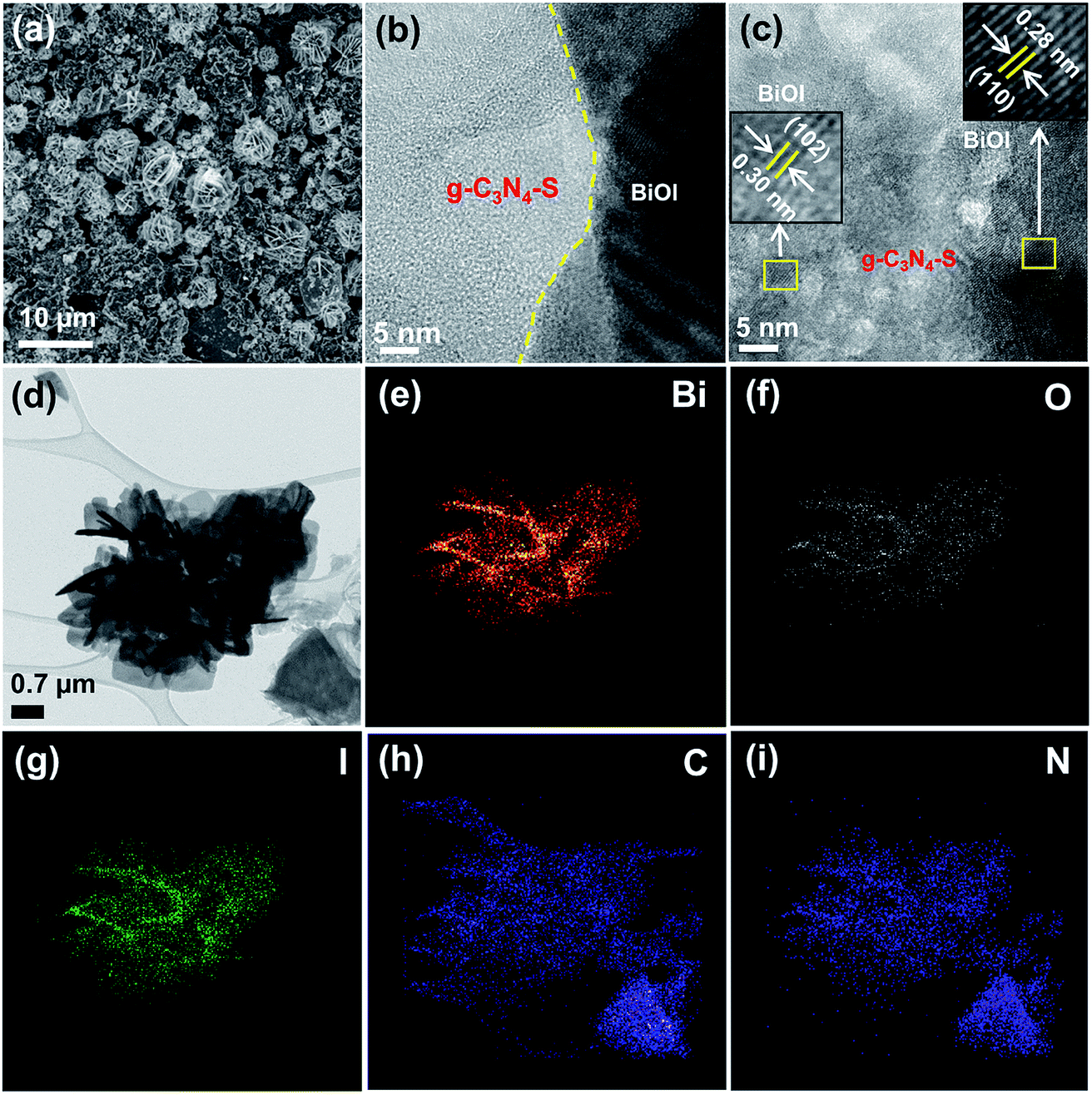 | ||
| Fig. 2 (a) FESEM image of g-C3N4-S/BiOI thin film (b) HRTEM image showing heterojunction of BiOI and g-C3N4-S (c) HRTEM image showing lattice fringes (and insets showing d-spacing) corresponding to g-C3N4-S and BiOI (d) bright field STEM image of g-C3N4-S/BiOI; STEM elemental mapping for (e) Bi, (f) O, (g) I, (h) C and (i) N. | ||
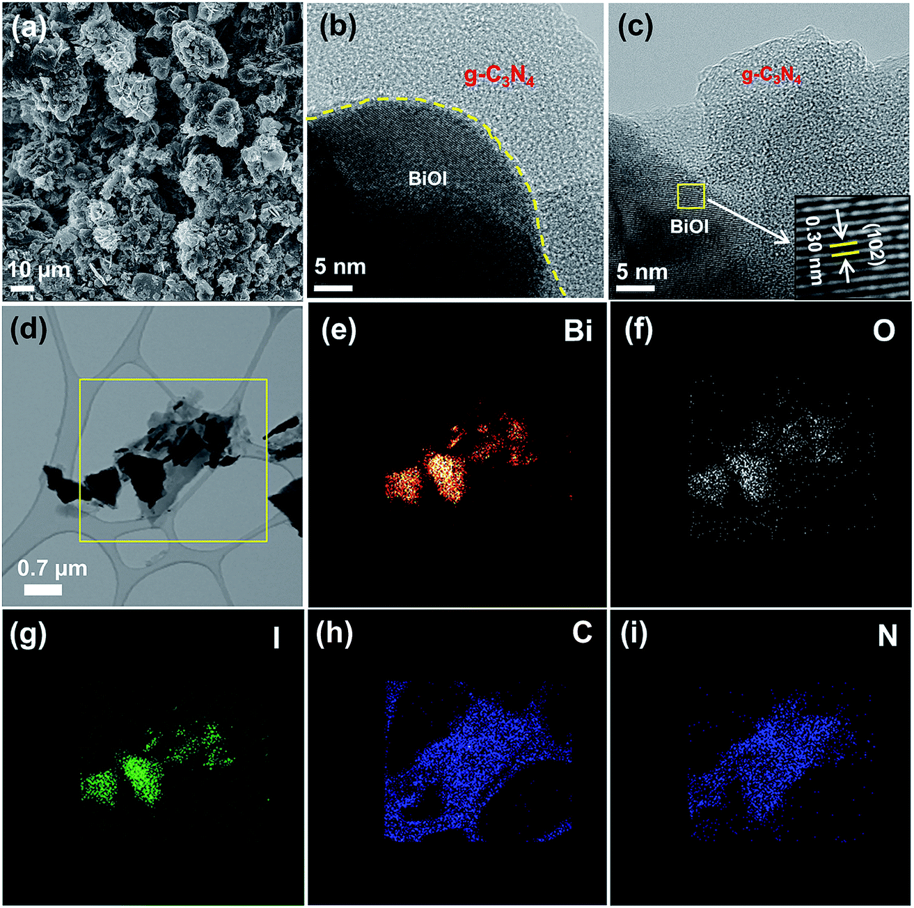 | ||
| Fig. 3 (a) FESEM image of g-C3N4-S/BiOI thin film and HR-TEM of g-C3N4-S/BiOI images at (b) 5 nm scale bar showing heterojunction of BiOI and g-C3N4-S, (c) at 5 nm scale bar showing lattice fringes and insets shows d-spacing corresponding to g-C3N4-S and BiOI, (d) bright field STEM image of g-C3N4-S/BiOI, and STEM elemental mapping for (e) Bi, (f) O, (g) I, (h) C, (i) N. | ||
Fig. 4a displays the XRD patterns of bulk graphitic carbon nitrides (g-C3N4), few layered graphitic carbon nitride sheets (g-C3N4-S), bismuth oxyiodide and two heterojunctions (g-C3N4/BiOI and g-C3N4-S/BiOI). g-C3N4 and g-C3N4-S show a broad peak centered at ∼26° corresponding to the (002) plane originated from interlayer stacking of conjugated aromatic sheets and another small peak at 13.2° corresponding to (100) plane was specific to in-plane repetition of tri-s-triazine unit in the carbon nitride scaffold respectively.8 In the composite materials with BiOI, both (002) and (100) peaks appear, indicative of their preserved crystal structures. The diffractogram of pristine BiOI shows strong peaks characteristic of the tetragonal phase28 and all these peaks appear for both composites, albeit with significantly lower intensities for g-C3N4/BiOI compared to g-C3N4-S/BiOI. It is worth noting that the BiOI peak for the (001) plane does not appear in g-C3N4/BiOI. BiOI has two phases that have small difference. Both phases have a 2D structure along c axis and crystallize in the tetragonal space group P4/nmm. The difference between the two phases lies is the length of c axis (7.21 and 9.14 Å). The phase that shows stronger (001) plane, has shorter c axis length.28 The disappearance of the (001) plane in g-C3N4/BiOI might be due to (i) the reduction of the BiOI phase that shows (001) plane compared to the other phase due to coupling of (001) plane of BiOI with g-C3N4 leading to increased ratio of BiOI with longer c axis or (ii) the BiOI nanoplates have higher agglomeration in the g-C3N4/BiOI nanocomposite which might be responsible for shielding some signal,28 while in g-C3N4-S/BiOI the shielding of signals remain less prominent.
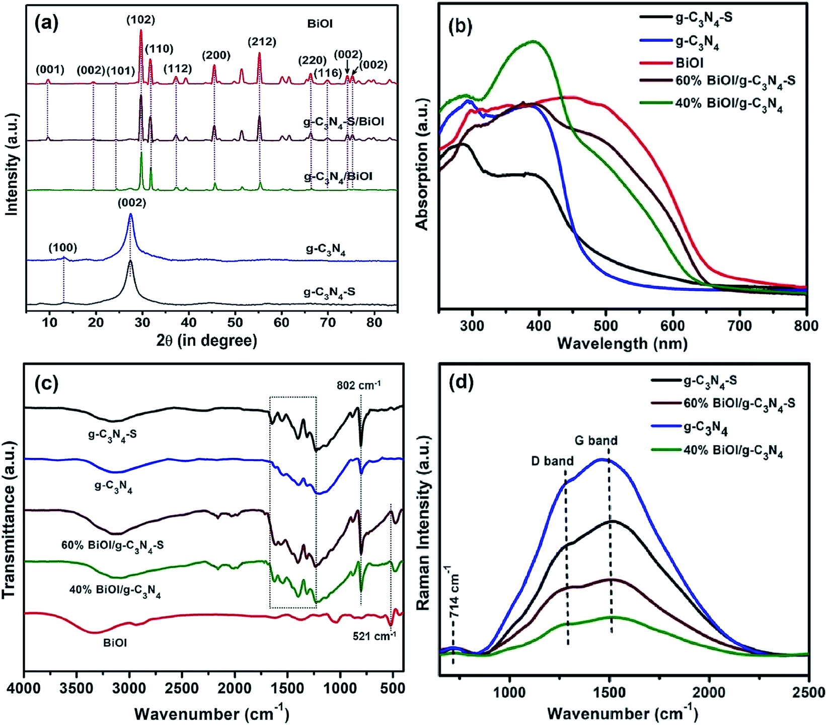 | ||
| Fig. 4 (a) X-ray diffractograms of pristine BiOI, g-C3N4-S/BiOI, g-C3N4/BiOI composites, pristine g-C3N4 (blue) and pristine g-C3N4-S (black) (b) UV-Vis absorption spectra collected in DRS mode (c) FTIR transmission spectra of pristine g-C3N4-S, pristine g-C3N4, g-C3N4-S/BiOI, g-C3N4/BiOI and pristine BiOI (d) Raman spectra (λexc = 780 nm) of pristine g-C3N4-S, pristine g-C3N4, g-C3N4-S/BiOI and g-C3N4/BiOI heterostructures. Color: BiOI (red), g-C3N4-S/BiOI (wine red), g-C3N4/BiOI (green) and g-C3N4-S (black). | ||
Fig. 4b shows the absorption spectra of the five different samples (pristine BiOI, pristine g-C3N4-S, pristine g-C3N4, g-C3N4-S/BiOI and g-C3N4/BiOI composites). The large bandgaps of g-C3N4-S and g-C3N4 significantly limits their response at longer wavelengths, while their heterostructures with BiOI certainly have more potential to be a superior photocatalyst. Bulk carbon nitride (g-C3N4) shows an absorption band around 270 nm due π → π* transition while another band around 390 nm with band tailing extended up to 500 nm originates from the n → π* transition.34 While both absorption bands were present for few-layered g-C3N4-S, the primary band edge was decreased to 450 nm which was attributed to the quantum confinement effect in few layer sheets.20 For the composites, two clear band edges, corresponding to BiOI and carbon nitride, can be seen from the plots. Pristine BiOI exhibits a band-edge at ∼680 nm with considerable sub-gap absorption extending to 800 nm due to trap states. This sub-gap absorption is suppressed in both g-C3N4-S/BiOI and the g-C3N4/BiOI, suggesting synergistic trap passivation in the nanocomposite heterostructures. Additionally, bandgaps of the investigated materials were estimated using Tauc plots by extrapolating the linear region of graph between (αhν)1/2vs. hν on abscissa where α is the absorption coefficient, h is Planck's constant and ν is the light frequency. From the Tauc plots, the values of the electronic bandgap for BiOI and g-C3N4 were found to be 1.74 and 2.55 eV respectively while for the few-layered carbon nitride (g-C3N4-S), the bandgap was reduced to 2.22 eV due to the formation of sheets (Fig. S4, see ESI†). After hybridization with low bandgap BiOI, the obtained effective bandgap values of the g-C3N4-S/BiOI and g-C3N4/BiOI heterostructures were found to be 1.79 and 1.84 eV respectively.
Fourier transform infrared spectroscopy (FTIR) was performed to discern the presence of various chemical functionalities in the nanocomposites. The FTIR peaks in 1240 and 1640 cm−1 region for g-C3N4-S and g-C3N4 were assigned to carbon nitride heterocycle (C–N) stretching modes.35 The other characteristic breathing mode observed at 802 cm−1 originated due to bending vibration of s-triazine units (Fig. 4c).36,37 BiOI displays a characteristic peak at 521 cm−1 due Bi–O stretch and appearance of this peak in g-C3N4-S/BiOI and g-C3N4/BiOI composites confirms the presence BiOI in the carbon nitride scaffold.38 Unlike previously reported work,26 we observe a small shift of this peak towards lower wavenumbers which might be due to interaction between BiOI and carbon nitrides.
Fig. 4d shows the Raman spectra for the pristine carbon nitrides (g-C3N4-S and g-C3N4) and their heterojunctions with BiOI. The two typical bands of carbon-based materials between 1300 and 1600 cm−1 can be found as D and G bands. The out of plane vibrations of sp3 carbon atoms give rise to the D band that represents defects and disorder, and the G band is assigned to E2g phonons which are the in-plane vibrations of sp2 carbon atoms characteristics of graphitic structure.39,40 Unlike graphene or graphene oxide materials, this bands are not very sharp for relatively amorphous carbon nitrides. The intensity ratio of these bands, ID/IG did not change noticeably in the heterostructures compared to the pristine carbon nitrides (Fig. 7b). This indicates no additional defects have been introduced into the carbon nitride framework in the composites, in other words the in-plane sp2 domain size remain unchanged. The small peak around 714 cm−1, which has been attributed to the out of plane C–C vibrations,41 can be seen as well in the spectrum of both pristine materials and their heterostructures.
3.2 Photocatalytic activity
The photoelectrochemical responses of the samples (pristine BiOI, pristine g-C3N4-S, pristine g-C3N4, g-C3N4-S/BiOI and g-C3N4/BiOI composites) were obtained under solar simulator (AM 1.5 G (one sun illumination)) using 0.1 M Na2SO4 as the electrolyte. Fig. 5a and b show that thin films of both the few layered graphitic carbon nitride sheets (g-C3N4-S) and the many layered bulk graphitic carbon nitride (g-C3N4) are unable to generate photocurrents higher than 0.20 mA cm−2 by themselves when used as photoanodes for water splitting. Similarly, the photocurrent density does not exceed 0.45 mA cm−2 when a pristine BiOI film is used as a stand-alone photoanode (Fig. 5c). However, a photoanode consisting of a nanocomposite film of BiOI and g-C3N4-S was able to generate a photocurrent density as high as 0.70 mA cm2 as seen in Fig. 5d. Such a > 50% increase in photoresponse over the pristine, low bandgap BiOI films is indicative of superior charge separation in the nanocomposite thin films. For the g-C3N4-S/BiOI composites, the highest photocurrent was observed for 60 wt% BiOI with g-C3N4-S and for g-C3N4/BiOI composites, 40 wt% BiOI with g-C3N4 gave the highest photocurrent. Light on–off experiments (Fig. 5) which demonstrate the photoresponse of the samples, were performed to investigate the charge separation efficiency under illumination. Fig. 5 shows a significant increase in the photocurrent for the heterostructures of carbon nitrides and BiOI compared to their pristine counterparts. These current values are the highest among all values reported thus far for these heterosystems.26–29 g-C3N4 and BiOI form a Type-II (staggered) heterojunction due to which photogenerated electrons in g-C3N4 are transferred to the BiOI while photogenerated holes in BiOI are transferred to g-C3N4.26,27 This enables both components of the heterojunction to harvest visible light and contribute towards the generation of photocurrent. The ABPE at 0.6 V vs. RHE (water oxidation potential) for BiOI, g-C3N4-S, g-C3N4, g-C3N4-S/BiOI and g-C3N4/BiOI was calculated to be 0.16, 0.05, 0.04, 0.25 and 0.19% respectively (Fig. S8, see ESI†).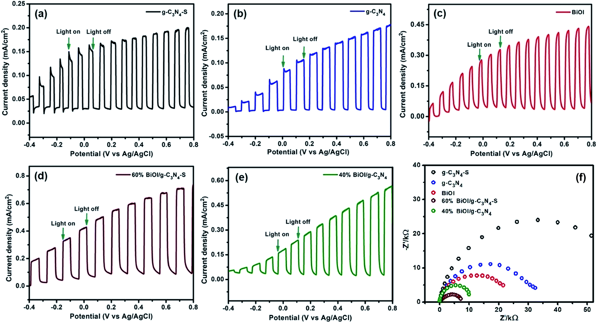 | ||
| Fig. 5 Light on–off experiment for (a) pristine g-C3N4-S (b) pristine g-C3N4 (c) pristine BiOI (d) g-C3N4-S/BiOI and (e) g-C3N4/BiOI; (f) Nyquist plots for the investigated samples obtained from EIS. | ||
Closer examination of the photoresponse curve in Fig. 5a reveals that the photocurrent decreases quickly and monotonically for the pristine g-C3N4-S thin film anode for small absolute values of applied bias (up to 0.3 V) whence the electric fields are not strong enough to enforce charge separation – a behavior characteristic of fast carrier recombination. Photocurrent values for the pristine BiOI film (Fig. 5c) do not saturate at a constant value for any value of applied bias during the on cycles and the photocurrent decays are slow during the off cycles, which constitute a signature of extensive trapping of charge carriers. Photocurrent values keep increasing with bias for the g-C3N4/BiOI nanocomposite thin film during the illumination on cycles for all values of bias (Fig. 5e), indicating that an intensifying semiconductor–electrolyte potential difference enhances the number of carriers extracted to perform useful work. On the other hand, photocurrent values increase with bias during the on cycles at applied voltages lower than 0.3 V for the g-C3N4-S/BiOI nanocomposite thin film (Fig. 5d) and then saturate for higher values of bias, indicating complete extraction of photogenerated charge carriers. The open circuit photovoltage values for pristine g-C3N4-S films, pristine g-C3N4 films and pristine BiOI films are −0.58 V, −0.50 V and −0.44 V respectively (vs. Ag/AgCl) while they are −0.56 V in the g-C3N4-S/BiOI nanocomposite thin film and −0.64 V in the g-C3N4/BiOI nanocomposite thin film. The significant shift in Voc for the g-C3N4/BiOI nanocomposite film over the Voc values of the pristine component films confirms increased band-bending and enhanced charge separation at the interface of the electrolyte and the g-C3N4/BiOI film while the lack of a similar shift in Voc for the g-C3N4-S/BiOI indicates the quasi-Fermi level of the nanocomposite film to be pinned to that of the g-C3N4-S film.
To probe the action of visible photons, we also carried out photoelectrochemical experiments under near-monochromatic 425 nm LED illumination (54.15 W cm −2) under identical conditions. It can be seen from Fig. S2 (see ESI†) that all the materials show a photoresponse for 425 nm irradiation. The highest photocurrent density (0.20 mA cm−2) was observed for the g-C3N4-S/BiOI heterostructure while a photocurrent density of 0.16 mA cm−2 was found for g-C3N4/BiOI which again confirms the symbiotic role of carbon nitride coupled with bismuth oxyiodide in increasing the photocurrent response. For pristine g-C3N4, g-C3N4-S and BiOI the value of photocurrent density was found to be 0.05, 0.04 and 0.09 mA cm−2 respectively. g-C3N4 (Fig. S2a, see ESI†) and g-C3N4-S (Fig. S2b, see ESI†) show transient photoconductivity profiles wherein upon light irradiation, an instantaneous rise in photocurrent was observed, which represents immediate generation of charge carriers and their motion resulting in a photocurrent density spike during the ON cycles. However, this spike suddenly decreased due to fast electron–hole recombination. A steady state photocurrent density was achieved once the rate of electron–hole pair generation and recombination reached a dynamic equilibrium.
For broad spectrum solar illumination, the bulk of the photons are absorbed by the smaller bandgap, more intensely absorbing BiOI component while both the g-C3N4 and BiOI components of the heterostructured nanocomposites absorb equally strongly at 425 nm. As a result, when illuminated by 425 nm photons, the J–V plots of g-C3N4-S/BiOI (Fig. S2d, see ESI†) and g-C3N4/BiOI (Fig. S2e, see ESI†) exhibited subtle but important differences with their J–V plots under broad spectrum AM1.5 one sun illumination (Fig. 5d and e respectively). During the light ON cycles, photocurrent spikes followed by a rapid decrease in current were seen under 425 nm illumination while the same was not seen under AM1.5 one sun illumination, indicating that recombination was stronger for carriers generated by 425 nm photons. This is because a major portion of the photogenerated minority carriers (holes) in g-C3N4 and g-C3N4-S experience fast recombination due to a large electron density and concomitant narrow space charge width, as will be shown in Sections 3.3, 3.4 and 3.5. On the other hand, photogenerated electron–hole pairs in BiOI are quickly separated by a strong built-in field, and the low electron density in BiOI means that minority carriers encounter fewer majority carriers to recombine with (see Sections 3.3 and 3.4).
3.3 Electrochemical properties
The semiconductor electrolyte interfacial (SEI) behavior for all the samples is represented by the Nyquist plots (Fig. 5f), which communicate information on the charge transfer resistance (Rct). Values of Rct can be equated with the diameters of the semicircular arcs denoting the Nyquist plots. As evident from the Nyquist plots, Rct decreased in the following order: g-C3N4-S > g-C3N4 > BiOI > g-C3N4/BiOI > g-C3N4-S/BiOI. This clearly shows the smaller charge transfer resistance of the nanocomposite heterostructures compared to pristine carbon nitrides. Detailed analysis of the SEI was performed by fitting the Nyquist plots to the equivalent circuit in Fig. S1 (see ESI†), which consists of Rct and the Helmholtz capacitance (Ch) in the low-frequency (0.1 to 100 Hz) region, a high-frequency (100 to 10![[thin space (1/6-em)]](https://www.rsc.org/images/entities/char_2009.gif) 000 Hz) time constant comprising the charge transport resistance (Rsc) and space charge capacitance (Csc), and an electrolyte resistance (Rs). The values of circuit parameters, obtained from the equivalent circuit (inset) of the semiconductor–electrolyte interface, are listed in Table 1. Charge transfer processes or diffusion of ions in solution near the SEI are generally slower than electronic processes within the semiconductor.42 Therefore, Ch and Rct were assigned to the low frequency response, and Rsc and Csc were assigned to the high-frequency region. The recombination lifetime (τ = RscCsc) values, obtained for the SEI, are in the range of several hundreds of milliseconds, and therefore, imply long-lived holes that promote the oxidation of water.43–46 Values of τ are listed in Table 1, and are in the following order: g-C3N4 > g-C3N4-S/BiOI > BiOI > g-C3N4/BiOI > g-C3N4-S. The very low value of Rct = 100 Ω for g-C3N4-S/BiOI (Table 1) and the saturation of the photocurrent at comparatively low bias values for g-C3N4-S/BiOI (Fig. 5d) indicates that photogenerated holes in this nanocomposite are able to reach the electrolyte before being captured into trap sites which in turn supports the previously mentioned symbiotic trap passivation effect in g-C3N4-S/BiOI.
000 Hz) time constant comprising the charge transport resistance (Rsc) and space charge capacitance (Csc), and an electrolyte resistance (Rs). The values of circuit parameters, obtained from the equivalent circuit (inset) of the semiconductor–electrolyte interface, are listed in Table 1. Charge transfer processes or diffusion of ions in solution near the SEI are generally slower than electronic processes within the semiconductor.42 Therefore, Ch and Rct were assigned to the low frequency response, and Rsc and Csc were assigned to the high-frequency region. The recombination lifetime (τ = RscCsc) values, obtained for the SEI, are in the range of several hundreds of milliseconds, and therefore, imply long-lived holes that promote the oxidation of water.43–46 Values of τ are listed in Table 1, and are in the following order: g-C3N4 > g-C3N4-S/BiOI > BiOI > g-C3N4/BiOI > g-C3N4-S. The very low value of Rct = 100 Ω for g-C3N4-S/BiOI (Table 1) and the saturation of the photocurrent at comparatively low bias values for g-C3N4-S/BiOI (Fig. 5d) indicates that photogenerated holes in this nanocomposite are able to reach the electrolyte before being captured into trap sites which in turn supports the previously mentioned symbiotic trap passivation effect in g-C3N4-S/BiOI.
| Sample | R s (ohms) | C h (F) | R ct (ohms) | C sc (F) | R sc (ohms) | τ (s) |
|---|---|---|---|---|---|---|
| g-C3N4-S | 1 | 0.000002 | 42000 |
0.000001 | 16500 |
0.0165 |
| g-C3N4 | 1 | 0.000035 | 20000 |
0.00001 | 10000 |
0.1000 |
| BiOI | 1 | 0.000023 | 15000 |
0.000006 | 7000 | 0.0420 |
| g-C3N4-S/BiOI | 1 | 0.000100 | 100 | 0.00001 | 10000 |
0.1000 |
| g-C3N4/BiOI | 1 | 0.000090 | 5000 | 0.00002 | 1500 | 0.0300 |
Charge carrier concentrations and flat band potentials of g-C3N4, g-C3N4-S, g-C3N4/BiOI (40% BiOI/g-C3N4), g-C3N4-S/BiOI (60% BiOI/g-C3N4-S), and BiOI were calculated using the Mott–Schottky relation, given by eqn (1).
 | (1) |
 | (2) |
In eqn (1), Csc is space-charge capacitance per unit area; εr the dielectric constant of the semiconductor (62 for g-C3N4,47 and 73 for BiOI48,49); ND is carrier concentration; ε0 is the vacuum permittivity (8.854 × 10⁻¹² F m−1); k is Boltzmann constant (1.381 × 10⁻²³ J K−1); T is temperature in (298 K); e is the electron charge (1.602 × 10⁻¹⁹ C); VFB is flat band potential; and V is the applied potential. ND, the charge carrier concentration, is calculated from the slope of the Mott–Schottky equations (eqn (1), using eqn (2)). VFB, the flat band potential is obtained the point of intersection of the slope (n in eqn (2)) with the potential axis as shown in the Mott–Schottky plots (Fig. 6 and S3, see ESI†).
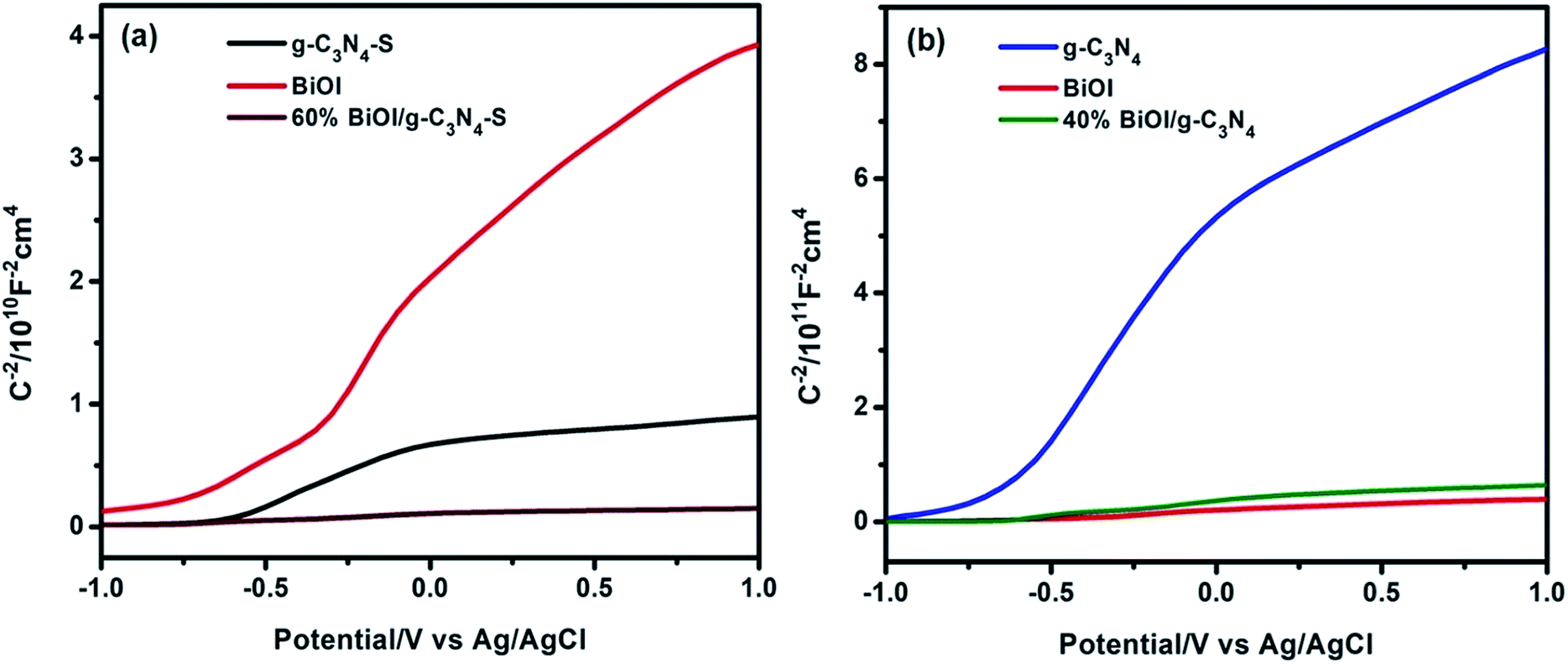 | ||
| Fig. 6 Mott–Schottky plots for (a) pristine g-C3N4-S, pristine BiOI and g-C3N4-S/BiOI and (b) pristine g-C3N4, pristine BiOI and g-C3N4/BiOI. The plots are shown in two different figures with two different scales (vertical axis) for improved visibility. | ||
According to Mott–Schottky plot (Fig. 6 and S3, see ESI†), all the semiconductor samples and their heterojunctions investigated in this study are n-type based on the positive slope of the C−2–V curves. As shown in Fig. S3,† the charge carrier density at equilibrium for g-C3N4-S is two orders of magnitude higher than that in g-C3N4, highlighting the distinct behavior of few-layer graphitic carbon nitride vs. many-layer bulk carbon nitride. Formation of the heterojunctions with BiOI increases the carrier density by nearly an order of magnitude (over the respective stand-alone photoanodes) for both the g-C3N4-S/BiOI and g-C3N4/BiOI heterostructure photoanodes, indicating the filling/elimination of electron traps which liberates mobile carriers available for conduction.
3.4 Photoluminescence and lifetime measurement
Fig. 7a shows the steady state photoluminescence (SSPL) spectra of the samples investigated in this work. The g-C3N4 and g-C3N4-S show intense PL peaks centered at 465 nm. The peak intensity of g-C3N4-S was relatively lower than bulk g-C3N4 which represent less prominent charge recombination attributed to better charge carrier separation in few layered sheets. The PL signals for g-C3N4-S/BiOI and g-C3N4/BiOI heterostructures were quenched significantly compared to the pristine carbon nitrides suggesting efficient charge transfer between BiOI and carbon nitrides. These results were in close agreement with the previously reported works.26,27 Small PL peak shift in g-C3N4-S/BiOI might originate due to electronic interaction between BiOI and few layered g-C3N4-S. To understand the nature of charge recombination processes and determine the lifetimes of excited species, time resolved photoluminescence (TRPL) spectra were measured. The obtained TRPL decay curves of all materials were fitted to a tri-exponential decay function of the form:| I(t) = A1e−t/τ1 + A2e−t/τ2 + A3e−t/τ3 | (3) |
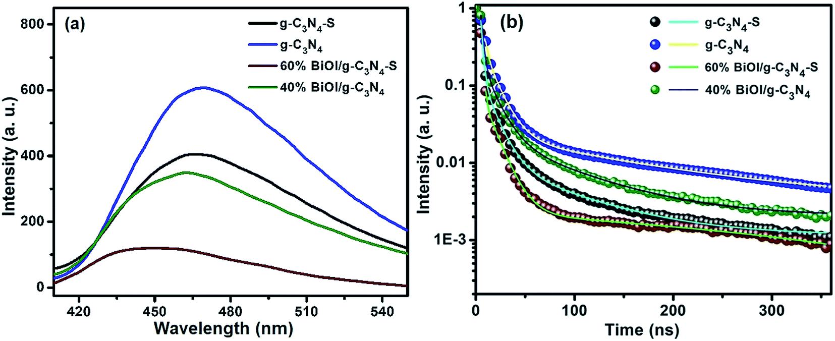 | ||
| Fig. 7 (a) Steady state PL spectra (λexc = 330 nm) for pristine g-C3N4-S, pristine g-C3N4, pristine BiOI, g-C3N4-S/BiOI and g-C3N4/BiOI. The PL spectrum of BiOI was very weak and is not shown. (b) Time resolved photoluminescence spectra (λexc = 405 nm) and (b) Raman spectra (λexc = 780 nm) of pristine g-C3N4-S, pristine g-C3N4, g-C3N4-S/BiOI and g-C3N4/BiOI heterostructures. | ||
| Sample | τ 1 (ns)/A1 | τ 2 (ns)/A2 | τ 3 (ns)/A3 | Average lifetime (τave) ns | Red. χ2 | Adj. R2 |
|---|---|---|---|---|---|---|
| g-C3N4-S | 74.545/0.0107 | 12.301/0.176 | 1.971/7.127 | 6.98 | 8.52 × 10⁻⁸ | 0.999 |
| g-C3N4 | 2.230/11.026 | 12.746/0.0496 | 144.472/0.021 | 16.8 | 3.24 × 10⁻⁸ | 0.999 |
| g-C3N4-S/BiOI | 3620.125/0.015 | 12.646/0.119 | 0.621/279136.0 | 1.75 | 1.19 × 10⁻⁷ | 0.999 |
| g-C3N4/BiOI | 12.770/0.268 | 73.59/0.023 | 2.213/5.803 | 10.95 | 1.33 × 10⁻⁷ | 0.999 |
For the bulk multi-layered g-C3N4, the first and relatively dominant PL decay component has a short lifetime of 2.23 ns, which was attributed due to direct band-to-band radiative recombination (antibonding π* MO → bonding π MO transition). The second PL decay component with intermediate lifetime (12.75 ns) appeared due to radiative decay of electrons from antibonding π* to LP orbitals via intersystem crossing.50 The third decay component with a relatively longer lifetime of 144.47 ns likely originated due to inter-sheet recombination processes. The few-layered carbon nitride (g-C3N4-S) has two lifetime components (1.97 ns and 12.30 ns), similar in relative intensity and duration to the two shorter lifetime components in multi-layered g-C3N4 and originates from the same electronic transitions. In contrast to multilayered g-C3N4, in few layered g-C3N4 sheets, the inter-sheet recombination is reduced resulting in the dramatically reduced relative intensity of the longest lifetime component in g-C3N4-S. While the values of the decay components for the g-C3N4 and BiOI composites (g-C3N4-S/BiOI and g-C3N4/BiOI) were changed to significant extents, the relative lifetime decays followed similar patterns to the pristine carbon nitride materials.
The average lifetime (τavg) was used to evaluate the effectiveness of charge separation in the heterostructures and was determined from the tri-exponential components using the following expression:
| τavg = (A1τ12 + A2τ22 + A3τ32)/(A1τ1 + A2τ2 + A3τ3) | (4) |
The average lifetimes of g-C3N4-S, g-C3N4, g-C3N4-S/BiOI and g-C3N4-S/BiOI were found to be 6.98, 16.80, 1.75 and 10.95 ns respectively. For BiOI and g-C3N4 composites (g-C3N4-S/BiOI and g-C3N4/BiOI), the average lifetimes are significantly decreased which is attributed to better charge separation in the nanocomposite. The decrease in PL lifetime was consistent with quenching in the steady state PL spectra.
3.5 Mechanism of photoresponse enhancement
Based on bandgap and band potential values, we have proposed a plausible mechanism responsible for the increase in photoelectrochemical water splitting performance. From the Tauc plot the bandgap (Eg) values for g-C3N4-S, g-C3N4 and BiOI were found to be 2.22, 2.55 and 1.74 eV respectively while the flat band potential values obtained from Mott–Schottky plot were found to be −0.66, −0.67 and −0.59 V vs. Ag/AgCl. The flat band potential can be considered as the position of the conduction band minimum (Ec) if the Fermi level lies just below the conduction band. Therefore, from the value of Eg and Ec, the position of the valence band maximum (Ev) for g-C3N4-S, g-C3N4 and BiOI were estimated to be +1.56, +1.88 and +1.35 V vs. Ag/AgCl. Usually in water splitting experiments, the standard redox potentials values are expressed on NHE scale so that the Ec positions of g-C3N4-S, g-C3N4 and BiOI were calculated to be −0.458, −0.474 and −0.391 V while the Ev positions were found to be +1.762, +2.076 and +1.548 V respectively on NHE scale at pH 0. To afford water splitting, the bandgap of material should be higher than 1.23 eV with the position of Ec more negative than 0.00 eV vs. NHE at pH-0 to facilitate reduction of protons (H+/H2) while the position of Ev should be more positive than 1.23 eV vs. NHE at pH-0 to achieve water oxidation (H2O/O2). Although the band edge positions of all the semiconductors in this study complied with the basic requirements of water splitting, individual components suffered from faster charge recombination processes. In bulk g-C3N4, the charge recombination process remains prevalent due to localized interlayer charge recombination. The transformation of bulk sheets into few layers break hydrogen bonds between sheets and increase crystallinity which resulted into better charge transportation on the surface of sheets. Consequently, heterojunction formation of BiOI with few layered g-C3N4-S afforded maximum performance in water splitting experiments. From Mott–Schottky plots (Fig. S4, see ESI†), it is evident that the synthesized BiOI has weaker n-type character than g-C3N4-S and its Fermi level lies lower than in g-C3N4-S. Heterojunction formation of BiOI with g-C3N4-S results in a flow of electrons from the CB of g-C3N4-S to the CB of BiOI due to Fermi level difference until equilibrium is reached (Fermi level alignment). This leads to the formation of a Type II (staggered) heterojunction as shown in Fig. 8 where photogenerated electrons migrate from BiOI to g-C3N4-S and travel through the external circuit to the platinum cathode to be used for the reduction of protons to hydrogen while holes in the VB of BiOI are used for the oxidation of water (or OH−). However, the depletion region that would occur as a consequence of the formation of a Type-II heterojunction between BiOI and g-C3N4-S would also be expected to reduce the electron density of the heterostructured nanocomposite (g-C3N4-S/BiOI) which does not occur; instead Mott–Schottky plots indicate both g-C3N4-S/BiOI and g-C3N4/BiOI to have an order of magnitude higher carrier density than g-C3N4-S and g-C3N4 (also supported by the observation in EIS of a lower charge transfer resistance in the composites and the UV-Vis spectral observation of the suppression of sub-gap absorption in the composites), which suggests a synergistic trap filling/trap elimination process in the heterostructured photoanodes that liberates mobile carriers and overwhelms the effect of formation of a Type-II heterojunction. It is demonstrated however that heterojunction formation of BiOI with g-C3N4-S promotes better charge separation and increases the visible light photoelectrochemical performance.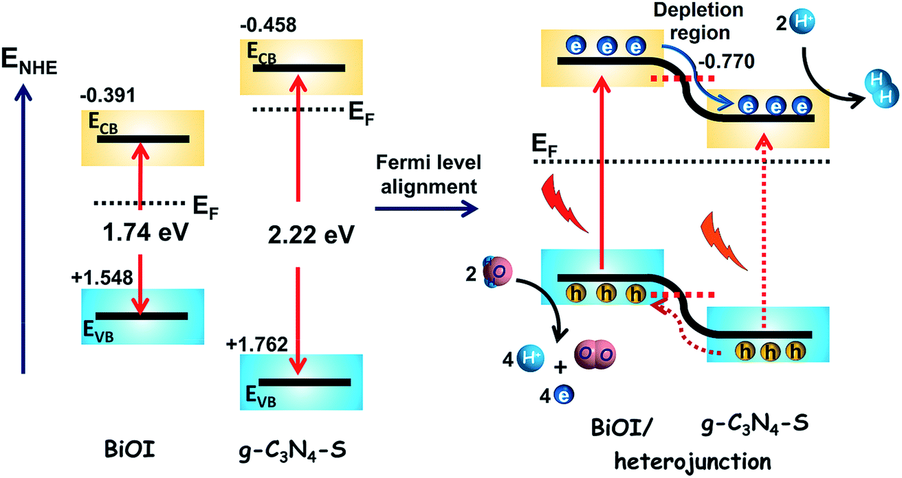 | ||
| Fig. 8 Proposed mechanism of charge separation in g-C3N4-S/BiOI heterostructured photoanodes. | ||
3.6 Reusability of the heterojunctions
In order to validate the long-term durability of g-C3N4-S/BiOI and g-C3N4/BiOI materials, we carried out reuse experiments. For the reuse experiment, FTO deposited material was washed with water and dried at 85 °C and reused for the measurement. The reuse results (Fig. S8, see ESI†) showed a negligible drop in the photocurrent response of heterostructured materials which is indicative of longevity and robustness. The used samples g-C3N4-S/BiOI and g-C3N4/BiOI composites were characterized with diffuse reflectance spectroscopy (DRS) absorption and XRD. Fig. S6 and S7 (see ESI†) show that these data are very similar to the freshly prepared samples. The composite catalysts remain unaffected in their chemical, optical and structural properties after several electrochemical cycles.4. Conclusion
We have explored the potential of two forms of graphitic carbon nitrides and their heterostructures with earth abundant bismuth oxyiodide. Few layered sheet-like carbon nitride (g-C3N4-S) exhibited higher crystallinity, lower inter-sheet recombination and higher carrier densities than multi-layered bulk g-C3N4. A significant enhancement in the photocurrent values was observed in the composites under simulated 1 sun illumination with the best performance provided by g-C3N4-S/BiOI heterostructured photoanodes. In the heterostructures – more effective charge separation, synergistic trap filling leading to a lower charge transfer resistance, and enhanced light absorption have been identified as dominant factors for the enhancement of photocurrent when compared to the pristine photoanodes. The Mott–Schottky plots revealed both carbon nitrides and bismuth oxyiodide to be n-type semiconductors. Based on the results of experimental characterization and analysis, we identified the mechanism for the electron–hole separation to be the transfer of photogenerated electrons in BiOI to g-C3N4-S through the formation of a Type II heterojunction interface. The heterostructured nanocomposites of graphitic carbon nitrides with bismuth oxyiodide displayed almost no loss in photoelectrochemical performance upon re-use and did not suffer damage to their structure and optical properties due to re-use, which bodes well for their long-term operational stability and durability.Conflicts of interest
There are no conflicts to declare.Acknowledgements
The authors thank NSERC, NRC, CMC Microsystems, Future Energy Systems and CFI for direct and indirect (equipment use) financial support. U. K. T. acknowledges scholarship support from Alberta Innovates. We acknowledge NRC-NINT and the UofA Nanofab for allowing usage of characterization facilities. Prof. Alkiviathes Meldrum is kindly acknowledged for allowing the use of the TRPL facility in his lab.References
- K. H. Akira Fujishima, Nature, 1972, 238, 37–38 CrossRef.
- A. J. Nozik, Annu. Rev. Phys. Chem., 1978, 29, 189–222 CrossRef CAS.
- M. Dahl, Y. Liu and Y. Yin, Chem. Rev., 2014, 114, 9853–9889 CrossRef CAS PubMed.
- P. Kar, Y. Zhang, S. Farsinezhad, A. Mohammadpour, B. D. Wiltshire, H. Sharma and K. Shankar, Chem. Commun., 2015, 51, 7816–7819 RSC.
- A. Naseri, M. Samadi, A. Pourjavadi, A. Z. Moshfegh and S. Ramakrishna, J. Mater. Chem. A, 2017, 5, 23406–23433 RSC.
- G. Yue, L. Wang, X. Wang, Y. Chen and D. Peng, Nanoscale Res. Lett., 2009, 4, 359 CrossRef CAS PubMed.
- S. Yin, J. Han, T. Zhou and R. Xu, Catal. Sci. Technol., 2015, 5, 5048–5061 RSC.
- A. Thomas, A. Fischer, F. Goettmann, M. Antonietti, J.-O. Müller, R. Schlögl and J. M. Carlsson, J. Mater. Chem., 2008, 18, 4893–4908 RSC.
- Y. Zheng, L. Lin, B. Wang and X. Wang, Angew. Chem., Int. Ed., 2015, 54, 12868–12884 CrossRef CAS PubMed.
- Q. Lin, L. Li, S. Liang, M. Liu, J. Bi and L. Wu, Appl. Catal., B, 2015, 163, 135–142 CrossRef CAS.
- X. Lu, K. Xu, P. Chen, K. Jia, S. Liu and C. Wu, J. Mater. Chem. A, 2014, 2, 18924–18928 RSC.
- M. R. Gholipour, F. Béland and T.-O. Do, ACS Sustainable Chem. Eng., 2016, 5, 213–220 CrossRef.
- P. Kumar, U. K. Thakur, K. Alam, P. Kar, R. Kisslinger, S. Zeng, S. Patel and K. Shankar, Carbon, 2018, 137, 174–187 CrossRef CAS.
- D. O. Adekoya, M. Tahir and N. A. S. Amin, J. CO2 Util., 2017, 18, 261–274 CrossRef CAS.
- B. Tahir, M. Tahir and N. A. S. Amin, Appl. Surf. Sci., 2017, 419, 875–885 CrossRef CAS.
- K. Schwinghammer, M. B. Mesch, V. Duppel, C. Ziegler, J. r. Senker and B. V. Lotsch, J. Am. Chem. Soc., 2014, 136, 1730–1733 CrossRef CAS PubMed.
- P. Kumar, R. Boukherroub and K. Shankar, J. Mater. Chem. A, 2018, 6, 12876–12931 RSC.
- W. Iqbal, B. Qiu, Q. Zhu, M. Xing and J. Zhang, Appl. Catal., B, 2018, 232, 306–313 CrossRef CAS.
- H. Ou, L. Lin, Y. Zheng, P. Yang, Y. Fang and X. Wang, Adv. Mater., 2017, 29, 1700008 CrossRef PubMed.
- S. Yang, Y. Gong, J. Zhang, L. Zhan, L. Ma, Z. Fang, R. Vajtai, X. Wang and P. M. Ajayan, Adv. Mater., 2013, 25, 2452–2456 CrossRef CAS PubMed.
- J. Zhang, Y. Chen and X. Wang, Energy Environ. Sci., 2015, 8, 3092–3108 RSC.
- D. S. Bhachu, S. J. A. Moniz, S. Sathasivam, D. O. Scanlon, A. Walsh, S. M. Bawaked, M. Mokhtar, A. Y. Obaid, I. P. Parkin, J. Tang and C. J. Carmalt, Chem. Sci., 2016, 7, 4832–4841 RSC.
- H. Cheng, B. Huang and Y. Dai, Nanoscale, 2014, 6, 2009–2026 RSC.
- M. Guan, C. Xiao, J. Zhang, S. Fan, R. An, Q. Cheng, J. Xie, M. Zhou, B. Ye and Y. Xie, J. Am. Chem. Soc., 2013, 135, 10411–10417 CrossRef CAS PubMed.
- Z. A. Xi Zhang, F. Jia and L. Zhang, J. Phys. Chem. C, 2008, 112, 747–753 CrossRef.
- J. Di, J. Xia, S. Yin, H. Xu, L. Xu, Y. Xu, M. He and H. Li, J. Mater. Chem. A, 2014, 2, 5340–5351 RSC.
- S.-Y. Chou, C.-C. Chen, Y.-M. Dai, J.-H. Lin and W. W. Lee, RSC Adv., 2016, 6, 33478–33491 RSC.
- J. C. Wang, H. C. Yao, Z. Y. Fan, L. Zhang, J. S. Wang, S. Q. Zang and Z. J. Li, ACS Appl. Mater. Interfaces, 2016, 8, 3765–3775 CrossRef CAS PubMed.
- H. An, B. Lin, C. Xue, X. Yan, Y. Dai, J. Wei and G. Yang, Chin. J. Catal., 2018, 39, 654–663 CrossRef CAS.
- C. Chang, L. Zhu, S. Wang, X. Chu and L. Yue, ACS Appl. Mater. Interfaces, 2014, 6, 5083–5093 CrossRef CAS PubMed.
- L. Xu, P. Yan, H. Li, S. Ling, J. Xia, Q. Xu, J. Qiu and H. Li, RSC Adv., 2017, 7, 7929–7935 RSC.
- U. K. Thakur, A. M. Askar, R. Kisslinger, B. D. Wiltshire, P. Kar and K. Shankar, Nanotechnology, 2017, 28, 274001 CrossRef PubMed.
- C. Pan, J. Xu, Y. Wang, D. Li and Y. Zhu, Adv. Funct. Mater., 2012, 22, 1518–1524 CrossRef CAS.
- A. Kumar, P. Kumar, C. Joshi, S. Ponnada, A. K. Pathak, A. Ali, B. Sreedhar and S. L. Jain, Green Chem., 2016, 18, 2514–2521 RSC.
- S. C. Yan, Z. S. Li and Z. G. Zou, Langmuir, 2009, 25, 10397–10401 CrossRef CAS PubMed.
- Y. Wang, R. Shi, J. Lin and Y. Zhu, Energy Environ. Sci., 2011, 4, 2922–2929 RSC.
- J. Zhang, M. Zhang, G. Zhang and X. Wang, ACS Catal., 2012, 2, 940–948 CrossRef CAS.
- S.-T. Huang, Y.-R. Jiang, S.-Y. Chou, Y.-M. Dai and C.-C. Chen, J. Mol. Catal. A: Chem., 2014, 391, 105–120 CrossRef CAS.
- A. C. F. a. J. Robertson, Phys. Rev. B: Condens. Matter Mater. Phys., 2000, 61, 14095–14107 CrossRef.
- M. S. Dresselhaus, A. Jorio, M. Hofmann, G. Dresselhaus and R. Saito, Nano Lett., 2010, 10, 751–758 CrossRef CAS PubMed.
- A. K. M. S. Chowdhury, D. C. Cameron and M. S. J. Hashmi, Thin Solid Films, 1998, 332, 62–68 CrossRef CAS.
- T. Lopes, L. Andrade, F. Le Formal, M. Gratzel, K. Sivula and A. Mendes, Phys. Chem. Chem. Phys., 2014, 16, 16515–16523 RSC.
- A. J. Cowan, C. J. Barnett, S. R. Pendlebury, M. Barroso, K. Sivula, M. Grätzel, J. R. Durrant and D. R. Klug, J. Am. Chem. Soc., 2011, 133, 10134–10140 CrossRef CAS PubMed.
- M. Barroso, S. R. Pendlebury, A. J. Cowan and J. R. Durrant, Chem. Sci., 2013, 4, 2724–2734 RSC.
- F. M. Pesci, G. Wang, D. R. Klug, Y. Li and A. J. Cowan, J. Phys. Chem. C, 2013, 117, 25837–25844 CrossRef CAS PubMed.
- I. Concina, Z. H. Ibupoto and A. Vomiero, Adv. Energy Mater., 2017, 7, 1700706 CrossRef.
- S. Pareek and J. K. Quamara, J. Mater. Sci., 2018, 53, 604–612 CrossRef CAS.
- J. Hu, S. Weng, Z. Zheng, Z. Pei, M. Huang and P. Liu, J. Hazard. Mater., 2014, 264, 293–302 CrossRef CAS PubMed.
- N. T. Hahn, S. Hoang, J. L. Self and C. B. Mullins, ACS Nano, 2012, 6, 7712–7722 CrossRef CAS PubMed.
- Y. Zhang, Q. Pan, G. Chai, M. Liang, G. Dong, Q. Zhang and J. Qiu, Sci. Rep., 2013, 3, 1943 CrossRef PubMed.
Footnotes |
| † Electronic supplementary information (ESI) available. See DOI: 10.1039/c8na00264a |
| ‡ These authors contributed equally. |
| This journal is © The Royal Society of Chemistry 2019 |