
When defects become ‘dynamic’: halide perovskites: a new window on materials?†
Yevgeny
Rakita
 ,
Igor
Lubomirsky
and
David
Cahen
*
,
Igor
Lubomirsky
and
David
Cahen
*
Materials and Interfaces Dept., Weizmann Institute of Science, Rehovot, 76100, Israel. E-mail: david.cahen@weizmann.ac.il; igor.lubomirsky@weizmann.ac.il; yevgev@gmail.com
First published on 28th June 2019
Abstract
Although Pb Halide perovskites (HaPs) can be prepared as organic electronic materials, they resemble top-quality inorganic semiconductors, especially with respect to their low defect densities, as derived from optical and electronic transport studies. Among causes for such low defect densities were ‘defect-tolerance’ (proposed) and ‘self-healing’ (experimentally identified). We show that HaPs are likely an example of a class of materials that cannot support static bulk defect densities significantly above thermodynamically-dictated densities. The reasons are (a) the free energy to form HaPs (from binary halides) is less than the formation energies of (static) defects in them and (b) the small kinetic stabilization of such defects. We summarize the evidence for such a situation and conclude that higher defect densities in polycrystalline films likely result from the (expected) smaller defect formation energy at surfaces and grain boundaries than in the bulk. This situation directly limits the options for doping such materials, and leads to the counter-intuitive conclusion that a low free energy of formation (from the binaries) can lead to self-healing and, consequently, to low densities of static defects, to be distinguished from dynamic ones. The latter can be benign in terms of (opto)electronic performance, because of their relatively short lifetimes. We propose that the conditions that we formulated can serve as search criteria for other low defect density materials, which can be of interest and beneficial, also for applications beyond optoelectronics.
Background
For (opto)electronic functions of semiconductors, structural defects (in the bulk and/or at their surfaces/interfaces) are often of decisive importance (see the ESI,† i). Free electronic charge carriers with energies at/near conduction or valence band extrema are prone to interact with structural defects. Defects can trap (localize) charge carriers and/or facilitate their mutual annihilation (i.e., electron–hole recombination). Defects, charged or neutral, may act (alongside lattice vibrations) as scattering centers for carriers during their transport and thus, reduce carrier mobility; all these processes are usually detrimental for (opto)electronics.1,2We associate defects in what we will call ‘classical’ semiconductors (like Si, GaAs, with tetrahedral coordination), with missing or extra atoms, where the extra ones can also be extrinsic, i.e., different from the atoms making up the semiconductor. All such defects often have electronic states inside the bandgap, EG. For example, B or P in Si form p- or n-Si, respectively, via formation of states that have energies close to the valence band maximum, VBM, or conduction band minimum, CBM of Si, respectively, the so-called shallow defects. For a material such as CuInSe2, intrinsic defects, primarily In on a Cu site, InCu, and Cu vacancies, VCu, determine its doping. The electronic states associated with these dopants affect the electronic carrier density, as usually observed in a (logarithmic) increase of conductivity with carrier concentration over 5–7 orders of magnitude.3
In general, one will try to minimize defects, which in extremum, becomes a very demanding task. Importantly, we can prepare materials that are spatially heterogeneous in terms of doping, with a p–n junction as the best-known example. Spatial heterogeneity is possible only because the relevant dopants (i.e., defects) do not move on practical time-scales over significant distances, around the operating temperatures of the doped material: the defects are ‘kinetically stabilized’. Such defects cannot move to annihilate each other, or be annihilated by reaching the surface, as the ‘activation energy’, Ea for their migration is too high compared to kBT, with kB Boltzmann's constant and T the operating temperature, in K. Increasing the temperature can decrease the defect density in a process called annealing, which means here that defects can be eliminated, allowing the system to get closer to its thermodynamic equilibrium state. That state will always contain some defects because of the entropy associated with their presence (cf.Fig. 1(i)). Beyond the thermodynamically-dictated minimal defect density (which depends on the enthalpy of formation of the defect and on temperature), additional defect formation implies that the enthalpy of defect formation is smaller than that related to any form of decomposition of the material.
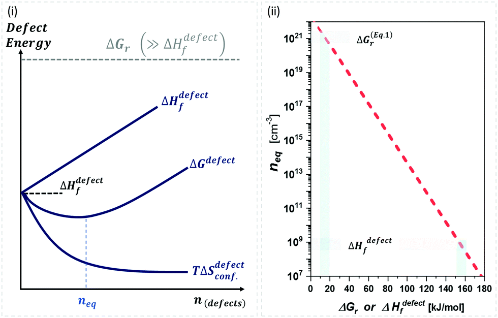 | ||
Fig. 1 (i) General scheme for thermodynamically-imposed point defect density (n) of a system at a finite temperature, if |ΔGr| ≫ ΔHdefectf. As defect density increases ‘enthalpy’ (ΔHdefectf) is invested for each defect, but ‘entropic energy’ (TΔSdefectconf.) is gained, so that the overall ‘free energy’ of the system (ΔG = ΔGr + ΔGdefect = ΔH − TΔS) has a minimum at a finite defect density (neq). (ii) Estimates of the equilibrium defect densities, neq, at T = 300 K for common intrinsic point defects: Schottky-pair (a pair of oppositely charged ionic vacancies) or Frenkel defect (displacement of atom into interstitial site, creating a vacancy), where  (see the ESI,† x). The pre-exponential factor contains the lattice parameter (a) and the number of lattice/interstitial sites that can become a defect (N),34 and was chosen for cubic MAPbX3 (with a ∼ 0.63 nm and N ∼ 6). Similar results are obtained for other HaPs. The pale-blue and gray bars are guides to the eye for the defect formation energy (ΔHdefectf ∼ 160 kJ mol−1), using the value for VBr in PbBr2,31 and for MAPbX3 dissociation (ΔGeqn (see the ESI,† x). The pre-exponential factor contains the lattice parameter (a) and the number of lattice/interstitial sites that can become a defect (N),34 and was chosen for cubic MAPbX3 (with a ∼ 0.63 nm and N ∼ 6). Similar results are obtained for other HaPs. The pale-blue and gray bars are guides to the eye for the defect formation energy (ΔHdefectf ∼ 160 kJ mol−1), using the value for VBr in PbBr2,31 and for MAPbX3 dissociation (ΔGeqn![[thin space (1/6-em)]](https://www.rsc.org/images/entities/char_2009.gif) (1)r ∼ 10–20 kJ mol−1).25 (1)r ∼ 10–20 kJ mol−1).25 | ||
Here we show how the very low bulk defect densities of halide perovskites, can be readily understood within the context of energies of activation and formation of (de)composition and possible defects, which, thus, suggests a new path to defect management in materials.
Halide perovskites (HaPs)
HaPs are materials with ABX3 stoichiometry (A, B mono-, di-valent cations, resp.; X halide anion) that, with B = Pb can perform close to, or like those made with known high-quality semiconductors. This is so, even though they can be prepared by low temperature synthesis, a route that normally implies poor semiconductor quality.Energies, densities and cross-sections for scattering of electrically-active defects can be deduced from experiments such as Space Charge Limited Current, SCLC (on a device structure), Thermally Stimulated Current, TSC, Deep Level Transient Spectroscopy, DLTS, and others.4–9 The use of such methods on HaPs, especially MAPbBr3 and MAPbI3 (where MA = CH3NH3+) yields remarkably low densities of ∼1010 cm−3 for (low temperature, solution-grown) single crystals and at most ∼1016 cm−3 and usually less (down to 1013 cm−3 for vacuum evaporated MAPbI3) for polycrystalline thin films.10,11 The difference between these two densities can be attributed to surface and/or grain-boundary defects, as for the mm- or larger-sized single crystals, the densities, deduced from the measurements, should be due mainly to bulk defects. Similar low densities of defects (∼1010 cm−3) in other semiconductors are possible (e.g., ultra-pure Si, or epitaxially-grown GaAs),9 but require significant efforts/advanced apparatus, involving increased temperatures; HaPs seem to be much more forgiving than classical semiconductors to specific growth or deposition paths.
Low cross-sections of interaction between electronic charge carriers and defects is one way to explain the low densities, deduced for HaPs. Very shallow in-gap defect states (within a range of a few kBT of the VBM or CBM) or states with levels in the bands, the so-called resonances, in which carriers are delocalized within the crystal, should not interact with charge carriers, observable in a measurement that probes trap density; they will be ‘invisible’ in experiments used to determine defect densities (and energies).12,13 In HaPs and Pb-chalcogenides (PbX, X = S, Se or Te), the valence band may have ‘anti-bonding’, rather than the usual ‘bonding’ character,14,15 which can, theoretically, lead to such very shallow or resonant defect states.
Apart from that this idea that awaits experimental proof, attributing shallow defects in HaPs to an ‘anti-bonding’ VBM is limited to intrinsic defects and should not apply to extrinsic ones. Another issue with this concept is the low doping efficiency in HaPs, in sharp contrast with most ‘classical’ semiconductors. Even if shallow defects would not interact strongly with free charges, they should dope the material. However, extrinsic doping, with e.g., Bi3+ for Pb2+ in MAPbBr3 single crystals, should, at 1019 cm−3 doping, result in much more than the observed ∼2 orders of magnitude increase in conductivity.16,17 Similar examples of limited changes in HaP conductivity were also reported for exposure to I2 or O2.18,19 Making the reasonable, but yet to be proven assumption that some Bi3+ replaces Pb2+17 and considering the measured trap density of an intrinsic MAPbBr3 crystal (∼1010 cm−3), such doping is very inefficient (see the ESI,† ii). Similar low doping efficiencies are seen in chalcopyrites,20 amorphous Si or, earlier doping efforts in organic semiconductors.21,22
What may explain low trap densities and inefficient ‘doping’ is thermodynamic and kinetic instability of defects with respect to the free energy and activation energy for material decomposition.
Model
Thermodynamics of formation vs. decomposition
The stability of a system is defined by its free energy with respect to any dissociation reaction (here denoted by subscript ‘r’), e.g., ΔGr = ΔHr − TΔSr, where ΔHr and ΔSr are the enthalpy and entropy of the dissociation reaction, respectively. A compound will be called ‘stable’ if ΔGr is negative; spontaneous dissociation will occur eventually if ΔGr is positive. Thus, ΔGr is the free energy, resulting from the total enthalpy, ΔHr and entropic energy, TΔSr for the formation of the material from its constituents (see the ESI,† iii). ΔSr mostly results from vibrational, rather than configurational, entropy23 and for compounds with low ΔGr, adding mixing entropy may be important.In “classical” semiconductors ΔGr is dominated by the enthalpy (ΔHr); the entropic energy (TΔSr) plays a minor role in stabilizing the material, and can often be destabilizing. In long-chained molecules, especially proteins, entropy plays a major role in stabilizing and defining their final conformation.24 For semiconductors, though, it is very unusual to have entropic stabilization.
A recent review25 about the thermochemistry and calorimetry of HaPs clearly shows the difference between HaPs and “classical” semiconductors in terms of ΔGr, ΔHr and TΔSr. Considering the dissociation of MAPbX3 (MA = CH3NH3), eqn (1) describes the energetically most favorable path for dissociation into constituents. Below we write the chemical equation for the reverse, formation, reaction, to be consistent with common practice, where a negative sign of formation energy, −|ΔGr|, refers to a spontaneous reaction (see the ESI,† iv):
| PbX2(s) + MAX(s) → MAPbX3(s) | (1) |
The dissociation reaction is the opposite, i.e., reading eqn (1) from Right to Left (←), instead of from Left to Right (→). Overall, ΔGr (at 300 K) for MAPbI3 formation from its binaries is around ∼−10 kJ mol−1 (∼4 kBT at 300 K), slightly higher for MAPbBr3 and MAPbCl3 (∼−6.5 kBT and ∼−5.5 kBT, respectively)25 (see the ESI,† v). These results are also consistent with an earlier study of ours,26 showing that the total (free + activation) energy, needed to form MAPbI3 from its binaries (in isopropanol solution) is <20 kJ mol−1. This implies that any energy input >∼20 kJ mol−1 will locally decompose MAPbI3 into MAI and PbI2 (following eqn (1)).
With regard to the contributions of ΔHrvs. TΔSr to ΔGr, for MAPbI3 and MAPbBr3 (and less so for MAPbCl3) ΔHr of eqn (1) is positive or barely negative. To have negative ΔGr (and a stable compound), the entropic part must overcome the positive enthalpy (see the ESI,† vi). It is still possible, however, that the system will be kinetically stable, even with negative |ΔGr|, because thermodynamics tells us only what is possible and a reaction can be so slow that on a given time scale no reaction can be observed. For HaPs, nevertheless, the ease by which they can form tribochemically from their binaries (both organic27 and inorganic28), is, though, incompatible with kinetic stabilization. Adding to that result their ready formation by co-evaporation as well as from solution, strongly indicates that HaPs are stable thermodynamically, rather than kinetically.
Defect thermodynamics
Next we consider defect formation and define ΔGdefect as the free energy, including the enthalpy of defect formation, ΔHdefectf, and TΔSdefectconf., the configurational (also known as ‘mixing’) entropic energy that favors an increase in the number of defects. As noted, ΔGr values of HaPs are clearly different from those of ‘classical’ semiconductors, for which mostly |ΔGr| ≫ 10·kBT (see the ESI,† vii) and inequality| |ΔGr| ≫ ΔHdefectf | (2) |
 . Any defect density >neq must be kinetically stabilized.
Plotting neq (considering Schottky-pair or Frenkel type defects, common for ionic compounds), on a log scale vs. ΔHdefectf for cubic MAPbX3 (Fig. 1(ii)), shows that the experimentally-derived neq ∼ 109–1011 cm−3 for single crystalline HaPs9,10,29 corresponds to: ΔHdefectf ∼ 150 kJ mol−1 (1.60 eV) (see the ESI,† viii). Because for HaPs |ΔGr| ∼ 10–20 kJ mol−1 the inequality in eqn (2) does not hold.
Experimental defect data relevant to HaPs
While there are quite some computational theory studies on point defects in HaPs,30 the limited comparison with actual experimental data and the continuing improvement in methodologies (as well as the implicit use of a static defect model), lead us to focus on the (very few) experimental data on defects, relevant for HaPs, to test the suggested non-‘classical’ nature of defects in these materials.A combined impedance and isotope tracer study on PbBr2, the only Pb-halide for which this combination of experimental data exists till now, showed that Br− dominates ion conduction (Fig. 2(ii)).31 The activation energy, Ea, for Br− migration, derived from experiments that measure only ionic conductivity, is ∼30 kJ mol−1, while ΔHdefectf, deduced from radioactive 82Br isotope tracing, is ∼160 kJ mol−1 (see the ESI,† ix). If we use this value for VBr in MAPbBr3 (for lack of other options), then obviously, eqn (2) is not satisfied, which would imply that the ‘classical’ view of static point defects does not hold for this and similar HaPs. In the following we consider this possibility further:
 | ||
| Fig. 2 (i) Temperature dependence of Pb and Br diffusion coefficients in PbBr2, derived from isotope tracer and impedance experiments (reproduced with permission from ref. 31). The energies for activation (Ea = 0.31 eV = 30 kJ mol−1) and formation, (ΔHdefectf = 1.65 eV = 159 kJ mol−1) were deduced from the ionic and isotopic diffusion coefficients, Dionic(T), (from impedance measurements) and Diso.(T), respectively (see the ESI,† xii). (ii) Schematic representation of defects formed in (top) a ‘rigid’ lattice (e.g., ‘classical’ semiconductor), where |ΔGr| ≫ ΔHdefectf (kinetically stabilized material – blue dots) or (bottom) a ‘soft’ lattice with low energy for dissociation of the material, where |ΔGr| ≪ ΔHdefectf, e.g., in HaPs viaeqn (1) (thermodynamically-stabilized – yellow dots). | ||
The probability of finding defects in a lattice, P, can be represented by the ratio between defect density, n(defects), with the potential atomic sites that can become defects, N(sites). Thermodynamically, the origin of the defects does not matter, as formation of defects will always follow the most probable path, i.e., that of least resistance (with minimal energy requirement). Assuming a low activation energy for dissociation or a low barrier for diffusion (at most a few times kBT), formation of a defect in a periodic structure can lead to (i) a point defect that rapidly diffuse in space or (ii) dissociation/re-formation of the material:
 | (3i) |
 | (3ii) |
As illustrated in Fig. 2(ii), the probability of finding defects in ‘classical’ semiconductors will follow eqn 3(i) only if eqn (2) is satisfied. Then formation of ‘classical’ defects will not generate dissociation of the material, and with sufficient kinetic stabilization (usually the case in ‘classical’ semiconductors), the lifetime of such defects can be eons.32,33 Therefore, point defects in ‘classical’ semiconductors are usually present at densities well above their thermodynamic lower limit (neq in Fig. 1).
One indication that things may be different in HaPs comes from our experimental evidence for ‘self-healing’ in Br-based HaPs,35viz. after inflicting damage, the system can return to its original state (see the ESI,† xi). We connected this healing to the materials’ dynamic disorder, also termed ‘local polar fluctuations’.36 Therefore, in materials such as HaPs, where ΔHdefectf ≫ |ΔGr|, we suggest to view defects differently in terms of position, lifetime, and, likely, also in energy.37 As illustrated in Fig. 1(ii), the probability of finding a dynamic defect in HaPs, if the condition for eqn 3(ii) (ΔHdefectf ≫ |ΔGr|) holds, with ΔGr ∼ 10–20 kJ mol−1 is  ∼ few %, where Natoms ∼ 2 × 1022 cm−3 (see the ESI,† x), defects become ‘dynamic’, meaning, the lifetimes of the resulting defects must be much shorter than those of static ones (see below). If conditions for eqn 3(i) (ΔHdefectf ≪ |ΔGr|) would apply, then
 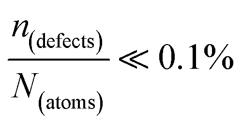 , but such defects should be viewed as static.
Interaction between defects and free charge carriers
We now consider the question of whether the defect's lifetime is long enough for free charges to interact with them. The point is that there is some characteristic lifetime for a defect, sufficiently long for a free charge to sense the defect's presence as different from the rest of the periodic bulk.When discussing lifetimes, we distinguish between two types of defects: (1) those that, to be eliminated, require mass diffusion over distances, sufficient to allow them to be expelled to the surface/interface; (2) defects that can form and recombine spontaneously within the bulk (without, or with minimal mass diffusion within nearest-neighbor distances), such as those that form as a result of decomposition (e.g., viaeqn (1)).
Referring to the latter, we consider ΔGeqn(1)r of HaPs (the defects illustrated in yellow in Fig. 2(ii)). These defects are the products of decomposition (viaeqn (1)), and will be referred to as ‘dynamic’ defects. The minimal interaction time for free charge carriers with defects should be many natural vibrations of the material. In HaPs, with a lowest (optical) phonon lifetime of ∼ps,38 this requires defects that exist for times ≫ps. In the next section we consider the lifetime of defects.
Dynamic and static defects
Considering the entropic stabilization of the material discussed earlier, lattice vibrations are usually viewed as the main contributors to the entropy of solids.23 Using the Debye frequency, ωD, which relates to the ‘attempt frequency’ for a reaction to occur, we can estimate an ‘effective’ defect lifetime: | (4) |
![[N with combining macron]](https://www.rsc.org/images/entities/b_i_char_004e_0304.gif) being an integer number of vibrations until a hoping event occurs, τD the Debye lifetime (= 1/ωD) and, for the current discussion, Ea = Eeqn(1)a is the activation energy for eqn (1) to occur. From previous work, we estimate Eeqn(1)a for MAPbI3 as <10 kJ mol−1,26 leading to the lifetime of a ‘dynamic defect’ of just several (<50) cycles of vibrations (which is sub-ps, taking38ωD ∼160 cm−1).
being an integer number of vibrations until a hoping event occurs, τD the Debye lifetime (= 1/ωD) and, for the current discussion, Ea = Eeqn(1)a is the activation energy for eqn (1) to occur. From previous work, we estimate Eeqn(1)a for MAPbI3 as <10 kJ mol−1,26 leading to the lifetime of a ‘dynamic defect’ of just several (<50) cycles of vibrations (which is sub-ps, taking38ωD ∼160 cm−1).
Following Almond and West,39 we find that this estimate of a defect's lifetime, or (1/τ(defect)), is equivalent to the hopping rate, ωp, that determines ion diffusion:
 | (5) |
 . In eqn (5)Ea = E(selfdiffusion)a refers to the activation energy for (ion) self-diffusion, meaning the rate at which defects diffuse and, eventually, can be eliminated at surfaces, or as clusters. Considering diffusion activation energies for HaPs as low as ∼30 kJ mol−1, the typical hopping lifetime is of the order of μs – already long enough for a free charge carrier to interact with a defect, which, in this respect, can be considered ‘static’. Still, in HaPs, similar to other solid electrolytes with Ea for self-diffusion <∼50 kJ mol−1, defects may diffuse within seconds–hours, leaving behind a ‘defect-free’ bulk material, consistent with the ‘self’ healing’, observed in the Br-HaPs.35 In ‘classical’ semiconductors, where Ea is of the order of several eV (in Si: Ea(S0i – self diffusion) ∼440 kJ mol−1; Ea(O0i) ∼240 kJ mol−1),40 at room temperature a single hopping event will, effectively, never occur without external stimulation. Thus, such defects are ‘kinetically-stabilized’.
Fig. 3 plots the result of eqn (4) and (5) as a function of the different activation energies (and temperatures), and vividly illustrates the differences in kinetic stabilization of defects in different semiconductor families. Comparing ‘dynamic’ and ‘static’ defects, there is a significant difference between the number of vibrations between a single hoping occurs, namely: (dynamic) ≪ (static), (dynamic) may decrease to only a few vibrational cycles, while (static) may be so large that on human timescales it is infinite, which we then refer to as a ‘kinetically-stabilized’ defect. The latter are the very basis for doping of semiconductors, optical defects in lasing materials and other cases where defects are crucial for the desired function of a material.
 | ||
| Fig. 3 (i) Number of vibrations before hopping (left axis) and time between hopping events (right axis) as a function of the activation energy for ion diffusion, following eqn (4) and (5) (dashed red line @ 300 K and shaded red dotted line @ 1200 K).39 Defects in Si, Cu(In,Ga)Se2 and HaPs are denoted by light blue bars; (ii) zoomed-in view of lower left corner of (i). The activation energies for HaPs in (ii) are divided into those for self- (ion-)diffusion, E(self-diffusion)a, and for (re)combination viaeqn (1), Eeqn(1)a. The right axis, which takes ωD in the THz frequency range,38 is a multiplication of the left axis by 10−12; thus, it represents the time between two dissociation or diffusion events in ∼s. The pale-blue and gray bars are guides to the eye for the different activation energies (cf. text). | ||
Effects of dynamic disorder & defects
Evidence that HaPs behave as dynamically structurally disordered materials was already derived from experimental and theoretical work.36,37,41–44 In such materials the average atomic position is ordered, so the FWHM of the (X-ray and neutron) diffraction peaks will be narrow and the optical absorption edge sharp,38,45 as long as the static disorder of the material is small (both are measurements taken over time scales ≫ωD−1, ∼THz). Therefore, if: (i) a defect is formed, but is not fixed in time and space; (ii) the measurement is slower than the time-dependent delocalization; (iii) the lattice fluctuations can “absorb” the strain that the delocalized defect will induce, i.e., low activation energy for delocalization of the defect, any interaction of free carriers with traps will become comparable to the transit time range of the lattice vibration, which will prevent defect energies from being experienced as different from those of the lattice (see the ESI,† xiii). Recent work by Ledinsky et al. experimentally separates the Urbach energy in parts due to ‘static’ and ‘dynamic’ defects.41 Comparing with ‘classic’ high-quality semiconductors, MAPbI3 shows the lowest ‘static’, but the highest ‘dynamic’ defect contribution to the Urbach energy.The practical implication of ‘dynamic’, but benign, defects is that they limit both ‘good’ (doping) and ‘bad’ (e.g., trapping) defect levels. Since doping requires ‘static’ defects, having ‘dynamic’ defects will not contribute to carrier density in the system. This can explain the preponderance of p-i-n structures in HaP-based devices;46–48 as the “i”-part can be very efficient for (especially) photovoltaics, this allows for good solar cells. Thus, likely, effective doping of such materials is possible primarily via their internal and external surfaces (see the ESI,† xiv). The fundamental regenerative capability of the bulk is another important reason why HaPs (see the ESI,† xv) are of great interest as radiation detectors,49–51 which usually require bulk single crystals with low carrier and (static) defect density.
Annealing, from static to dynamic
In cases where kinetic stabilization dominates, thermal annealing occurs when the activation barrier for recombination or diffusion of defects becomes comparable to the thermal energy of the system (∼few kBT), as also shown in the calculated plot in Fig. 3(i) (dashed line for 1200 K): upon increasing the temperature, τdefect, which scales exponentially with , becomes comparable to the lattice vibration time, ∼τD. Here Ea can be referred to as both Eeqn(1)a and E(selfdiffusion)a that are presented above.
We should emphasize that Eeqn(1)a, which is central to our model, differs from E(selfdiffusion)a. For the fate of extrinsic or intrinsic (any non-stoichiometry) defects, it is E(selfdiffusion)a that counts, as it defines the ability of a system to remove defects to a surface/interface. This process can be illustrated by the transformation of a kinetically-stabilized system, such as an amorphous material, to a crystalline one, where E(selfdiffusion)a is such that atom movement may become noticeable only after centuries or more, unless we heat. In HaPs, E(selfdiffusion)a is more like that for low temperature solid ion conductors (≤∼30 kJ mol−1), which allows defects to migrate at RT to a surface/interface within seconds.
In amorphous materials, like glassy (organic) polymers or inorganics, with large E(selfdiffusion)a, re-formation is usually more favorable than formation of point defects (see the ESI† xvi), leading to inefficient doping of amorphous systems (cf. a-Si).21 When an energy equivalent of a few times kBT approaches E(selfdiffusion)a (or Ea for material decomposition, in eqn (1)), an amorphous structure becomes entropically less favorable than higher symmetry crystalline forms and the transformation is a form of thermal annealing (cf.Fig. 4 – path (3) → (4)). In Pb HaPs |ΔGr| < E(selfdiffusion)a, so that ion displacement should lead to dissociation into PbX2 and AX (following eqn (1)), followed by a fast (entropy-driven) reconstruction to crystalline HaP.
 | ||
| Fig. 4 Schematic representation of (1) ‘static’ (‘classical’) semiconductors, SCs, (2) ‘dynamic’ (HaP-like), (3) ‘amorphous’ (glassy) and (4) annealed systems as a function of the ln of the probability, P, of finding a defect, ln(P) (eqn (3)), of the lifetime of a defect, ln(τ(defect) (eqn (4)), and the temperature of the system, T. The blue area represents the thermodynamic limit, above which systems are kinetically stabilized. The relative energies of ΔGr and Ea with respect to kBT will define whether defects in a system are ‘static’ (low density, long lifetime) or ‘dynamic’ (high density, short lifetime). The transition between a frozen (or an ‘amorphous’ (3)) state to a dynamically changing (or ‘annealing’ (4)) state, is determined by the temperature, where TCritical is a temperature of melting or decomposition. | ||
These four extreme cases of: (1) ‘static’ (‘classical’), (2) ‘dynamic’ (HaP-like), (3) ‘amorphous’ (glassy) and (4) annealed systems are summarized in a 3D plot (see the ESI,† xvii) of defect lifetime (eqn (4)) – probability (eqn (3)) – temperature in Fig. 4.
How different are HaPs from CuInSe2 (& CIGS)?
Similar to HaPs, the free energy of a reaction to compose CuInSe2 from its binaries: Cu2Se(s) and In2Se3(s) is very small, |ΔGr| ∼ 4 kJ mol−1 (or ∼2kBT), which, at increased temperatures, leads to its phase segregation into these binaries and a limited range of existence.52,53 Although doping chalcopyrites is more challenging than doping GaAs or Si, maximum carrier and defect densities of 1019 cm−3 can be reached;20,54,55 even in PV-quality films the carrier densities, 1017 cm−3, are still significantly higher than those of HaPs (1013–1016 cm−3). Interestingly, similar to ‘self-healing’ of HaPs that occurs at room temperature,35 defect ‘annealing’ is observed in Cu(In,Ga)Se2 thin films, but at ∼160 °C.56 The most important difference with HaPs is the activation energy for ion diffusion, which, at ∼1.1 eV57 is significantly higher than for HaPs (∼0.3 eV).31,58These data indicate that chalcopyrites are similar to HaPs thermodynamically, but not kinetically. They also drive home the point that while a small free energy of (de)composition is a necessary condition for a compound to be at its thermodynamic limit in terms of ‘static’ defect density, it is not a sufficient one: a low activation energy for (de)composition is also required.
Compounds for which both conditions are met will be prone to react with the ambient and to external stimuli such as irradiation. However, due to their dynamic nature, they can recover from inflicted damage under mild conditions, e.g., at low temperatures.
Surfaces, a limit on dynamic defect effects
It is important that we consider also the law of mass action and external impurities: if a material, like an HaP decomposes into its binaries,59,60 volatile constituents (e.g., halogens or organics for HaPs) can be released.61 These can also react with ambient impurities (e.g., O2).62 Even upon material loss or gain (introduction of extrinsic impurities, such as H2O, O2 or dopants), extrinsic point defects are still highly improbable to exist inside the bulk of HaP-like materials. However, due to low activation and formation energies, even if thermal or external factors (e.g., supra-bandgap illumination, electric field) create defects, these should be eliminated at surfaces/grain-boundaries or segregate, so that the bulk of the system will end up in a thermodynamically stable state, i.e., with the defect state described above.35 This is consistent with the narrow range of existence (with a narrow chemical potential window) of HaPs, as demonstrated both experimentally60,63 and theoretically,64,65 leading to phase segregation of PbX2 or AX2.At the same time a ∼0.5–1% change in the ratio of precursors significantly affects device performance.63 That result can be understood if, as has been argued, what dominates the performance of HaP-based devices is related to surface, grain boundary and interface effects, where formation and activation energies of defects are smaller than in the bulk66 (see the ESI,† xviii).
Summary
We showed how in HaPs defect densities, their dynamics, and their formation and activation energies connect. We explain this remarkable behavior of HaPs, based on their low formation energy and low kinetic barrier for formation from, and decomposition into their constituents and by a relatively high defect formation energy, but low activation energy for defect self-diffusion.Low formation energy from constituents, as well as entropic stabilization, suggest that whatever defect may exist in the structure momentarily, cannot be described within the commonly-used picture of a static defect, because its effective lifetime (and thus its interaction with free charge carriers) is so small that, effectively, it is non-existing for interaction with electronic charge carriers. We then connect these energetic considerations to measured defect densities.
For the Halide Perovskites the driving force to restore them from their binary constituents is mostly entropic. Based on the tribochemical27,28 and self-healing35,67 experimental results, we postulate that, at room temperature, entropy drives formation and regeneration of partially-organic and fully-inorganic HaPs. Since entropy dominates the material's stability, mixed HaPs (e.g., (Cs,MA,FA)Pb(I,Br)3) should be further stabilized, as suggested before,68 due to the additional component to the material's entropy.68 The basis for this experimentally observable extra stabilization is the mixing entropy ∼ kBT·ln(Xi) ≤ 2–4 kJ mol−1 (Xi = # of configurations). Usually this is insignificant, but if the system is only just stable, additional stabilization becomes very important.
We suggest to assess the potential of a system to have (HaP-like) benign ‘dynamic’ defects as follows:
– Free energy of formation with significant entropic stabilization.
– Activation energy for self-diffusion that is ≤∼30 kJ mol−1 (or ∼0.3 eV, ≤10 ∼ kBT@RT).
– If tribochemistry (mechanical grinding) of constituents results in a material with sharp diffraction peaks, there is a good chance that the system is entropically-stabilized with low activation energy for formation, which will result in low (static) bulk defect density.
– Generally, the lower the formal valency (e.g., monovalent halide vs. divalent oxides) and effective local (atomic) charge densities (large vs. small ion radius), the weaker the inter-atomic bonds and the smaller the electrostatic (Madelung energy); both these effects lead to lower enthalpy of formation and lower activation energy for atomic displacement.
– Systems that can decompose into constituents that do not require change in phase or oxidation state are likely to have low activation and formation energies for (de)composition.
– The higher the atoms’ coordination number, e.g., corner-sharing polyhedra vs. tetrahedra, the more likely the compound is to benefit from enhanced vibrational and configurational entropy (see the ESI,† vi).
Conflicts of interest
There are no conflicts to declare.Acknowledgements
We thank Davide Ceratti, Gary Hodes, Leeor Kronik, Omer Yaffe (Weizmann Inst.), Antoine Kahn, Sigurd Wagner (Princeton Univ.), David Egger (Regensburg) and Jean-Franois Guillemoles (IPVF, Paris) for fruitful discussions, Juan Bisquert (U Jaume II) for constructive criticism, and the Minerva (Munich) Centre for Self-Repairing Systems for Energy & Sustainability, at the Weizmann Institute, for partial support of this work.References
- S. Lany, Semiconducting transition metal oxides, J. Phys.: Condens. Matter, 2015, 27, 283203 CrossRef.
- J. I. Pankove, Optical Processes in Semiconductors, Courier Corporation, 1971.
- S. M. Sze and K. K. Ng, Physics of semiconductor devices, Wiley-Interscience, 2007.
- E. M. Hutter, G. E. Eperon, S. D. Stranks and T. J. Savenije, Charge Carriers in Planar and Meso-Structured Organic–Inorganic Perovskites: Mobilities, Lifetimes, and Concentrations of Trap States, J. Phys. Chem. Lett., 2015, 6, 3082–3090 CrossRef CAS.
- M. Jahandar, et al., High-Performance CH3NH3PbI3-Inverted Planar Perovskite Solar Cells with Fill Factor Over 83% via Excess Organic/Inorganic Halide, ACS Appl. Mater. Interfaces, 2017, 9, 35871–35879 CrossRef CAS PubMed.
- G. Gordillo, C. A. Otálora and M. A. Reinoso, Trap center study in hybrid organic-inorganic perovskite using thermally stimulated current (TSC) analysis, J. Appl. Phys., 2017, 122, 075304 CrossRef.
- J. W. Rosenberg, M. J. Legodi, Y. Rakita, D. Cahen and M. Diale, Laplace current deep level transient spectroscopy measurements of defect states in methylammonium lead bromide single crystals, J. Appl. Phys., 2017, 122, 145701 CrossRef.
- S. Heo, et al., Deep level trapped defect analysis in CH3NH3PbI3 perovskite solar cells by deep level transient spectroscopy, Energy Environ. Sci., 2017, 10, 1128–1133 RSC.
- D. Shi, et al., Low trap-state density and long carrier diffusion in organolead trihalide perovskite single crystals, Science, 2015, 347, 519–522 CrossRef CAS.
- T. M. Brenner, D. A. Egger, L. Kronik, G. Hodes and D. Cahen, Hybrid organic—inorganic perovskites: low-cost semiconductors with intriguing charge-transport properties, Nat. Rev. Mater., 2016, 16011 CrossRef.
- R. Babu, L. Giribabu and S. P. Singh, Recent Advances in Halide-Based Perovskite Crystals and Their Optoelectronic Applications, Cryst. Growth Des., 2018, 18, 2645–2664 CrossRef CAS.
- A. Zakutayev, et al., Defect Tolerant Semiconductors for Solar Energy Conversion, J. Phys. Chem. Lett., 2014, 5, 1117–1125 CrossRef CAS.
- M. V. Kovalenko, L. Protesescu and M. I. Bodnarchuk, Properties and potential optoelectronic applications of lead halide perovskite nanocrystals, Science, 2017, 358, 745–750 CrossRef CAS.
- W.-J. Yin, J.-H. Yang, J. Kang, Y. Yan and S.-H. Wei, Halide perovskite materials for solar cells: a theoretical review, J. Mater. Chem. A, 2015, 3, 8926–8942 RSC.
- Z.-Y. Ye, et al., The origin of electronic band structure anomaly in topological crystalline insulator group-IV tellurides, Npj Comput. Mater., 2015, 1, 15001 CrossRef CAS.
- A. L. Abdelhady, et al., Heterovalent Dopant Incorporation for Bandgap and Type Engineering of Perovskite Crystals, J. Phys. Chem. Lett., 2016, 7, 295–301 CrossRef CAS.
- P. K. Nayak, et al., Impact of Bi3+ Heterovalent Doping in Organic–Inorganic Metal Halide Perovskite Crystals, J. Am. Chem. Soc., 2018, 140, 574–577 CrossRef CAS.
- A. Zohar, et al., What Is the Mechanism of MAPbI3 p-Doping by I2? Insights from Optoelectronic Properties, ACS Energy Lett., 2017, 2, 2408–2414 CrossRef CAS.
- A. Zohar, et al., Impedance Spectroscopic Indication for Solid State Electrochemical Reaction in (CH3NH3)PbI3 Films, J. Phys. Chem. Lett., 2016, 7, 191–197 CrossRef CAS.
- S. B. Zhang, S.-H. Wei and A. Zunger, A phenomenological model for systematization and prediction of doping limits in II–VI and I–III–VI2 compounds, J. Appl. Phys., 1998, 83, 3192–3196 CrossRef CAS.
- M. Stutzmann, The doping efficiency in amorphous silicon and germanium, Philos. Mag. B, 1986, 53, L15–L21 CAS.
- I. Salzmann, G. Heimel, M. Oehzelt, S. Winkler and N. Koch, Molecular Electrical Doping of Organic Semiconductors: Fundamental Mechanisms and Emerging Dopant Design Rules, Acc. Chem. Res., 2016, 49, 370–378 CrossRef CAS.
- B. Fultz, Vibrational thermodynamics of materials, Prog. Mater. Sci., 2010, 55, 247–352 CrossRef CAS.
- S. Dagan, et al., Stabilization of a protein conferred by an increase in folded state entropy, Proc. Natl. Acad. Sci. U. S. A., 2013, 110, 10628–10633 CrossRef CAS.
- A. Ciccioli and A. Latini, Thermodynamics and the Intrinsic Stability of Lead Halide Perovskites CH3NH3PbX3, J. Phys. Chem. Lett., 2018, 9, 3756–3765 CrossRef CAS.
- T. M. Brenner, et al., Conversion of Single Crystalline PbI2 to CH3NH3PbI3: Structural Relations and Transformation Dynamics, Chem. Mater., 2016, 28, 6501–6510 CrossRef CAS.
- A. M. Elseman, M. M. Rashad and A. M. Hassan, Easily Attainable, Efficient Solar Cell with Mass Yield of Nanorod Single-Crystalline Organo-Metal Halide Perovskite Based on a Ball Milling Technique, ACS Sustainable Chem. Eng., 2016, 4, 4875–4886 CrossRef CAS.
- Z.-Y. Zhu, et al., Solvent-Free Mechanosynthesis of Composition-Tunable Cesium Lead Halide Perovskite Quantum Dots, J. Phys. Chem. Lett., 2017, 8, 1610–1614 CrossRef CAS.
- M. I. Saidaminov, et al., Inorganic Lead Halide Perovskite Single Crystals: Phase-Selective Low-Temperature Growth, Carrier Transport Properties, and Self-Powered Photodetection, Adv. Opt. Mater., 2017, 5, 1600704 CrossRef.
- C.-J. Yu, Advances in modelling and simulation of halide perovskites for solar cell applications, J. Phys. Energy, 2019, 1, 022001 CrossRef.
- S. R. Williams and L. W. Barr, A radioactive tracer study of diffusion processes in lead and silver bromide, J. Phys., Colloq., 1973, 34, C9-173–C9-177 Search PubMed.
- J. F. Guillemoles, I. Lubomirsky, I. Riess and D. Cahen, Thermodynamic Stability of p/n Junctions, J. Phys. Chem., 1995, 99, 14486–14493 CrossRef.
- I. Lubomirsky and D. Cahen, Chemical Limit to Semiconductor Device Miniaturization, Electrochem. Solid-State Lett., 1999, 2, 154–156 CrossRef CAS.
- J. S. Park, S. Kim, Z. Xie and A. Walsh, Point defect engineering in thin-film solar cells, Nat. Rev. Mater., 2018, 3, 194–210 CrossRef CAS.
- D. R. Ceratti, et al., Self-Healing Inside APbBr3 Halide Perovskite Crystals, Adv. Mater., 2018, 30, 1706273 CrossRef.
- O. Yaffe, et al., Local Polar Fluctuations in Lead Halide Perovskite Crystals, Phys. Rev. Lett., 2017, 118, 136001 CrossRef.
- A. V. Cohen, D. A. Egger, A. M. Rappe and L. Kronik, Breakdown of the static picture of defect energetics in halide perovskites: the case of the Br vacancy in CsPbBr3. ArXiv181004462 Cond-Mat, 2018.
- M. Sendner, et al., Optical phonons in methylammonium lead halide perovskites and implications for charge transport, Mater. Horiz., 2016, 3, 613–620 RSC.
- D. P. Almond and A. R. West, Mobile ion concentrations in solid electrolytes from an analysis of a.c. conductivity, Solid State Ionics, 1983, 9–10, 277–282 CrossRef CAS.
- S. K. Estreicher, D. J. Backlund, C. Carbogno and M. Scheffler, Activation Energies for Diffusion of Defects in Silicon: The Role of the Exchange-Correlation Functional, Angew. Chem., Int. Ed., 2011, 50, 10221–10225 CrossRef CAS.
- M. Ledinsky, et al., Temperature Dependence of the Urbach Energy in Lead Iodide Perovskites, J. Phys. Chem. Lett., 2019, 10, 1368–1373 CrossRef CAS.
- A. Poglitsch and D. Weber, Dynamic disorder in methylammoniumtrihalogenoplumbates (II) observed by millimeter-wave spectroscopy, J. Chem. Phys., 1987, 87, 6373–6378 CrossRef CAS.
- T. Baikie, et al., A combined single crystal neutron/X-ray diffraction and solid-state nuclear magnetic resonance study of the hybrid perovskites CH3NH3PbX3 (X = I, Br and Cl), J. Mater. Chem. A, 2015, 3, 9298–9307 RSC.
- P. S. Whitfield, et al., Structures, Phase Transitions and Tricritical Behavior of the Hybrid Perovskite Methyl Ammonium Lead Iodide, Sci. Rep., 2016, 6, 35685 CrossRef CAS.
- N. Onoda-Yamamuro, T. Matsuo and H. Suga, Calorimetric and IR spectroscopic studies of phase transitions in methylammonium trihalogenoplumbates (II), J. Phys. Chem. Solids, 1990, 51, 1383–1395 CrossRef CAS.
- E. Edri, et al., Elucidating the charge carrier separation and working mechanism of CH3NH3PbI3−xClx perovskite solar cells, Nat. Commun., 2014, 5, 3461 CrossRef.
- M. Kulbak, et al., Control over Self-Doping in High Band Gap Perovskite Films, Adv. Energy Mater., 2018, 8, 1800398 CrossRef.
- T. Wu, et al., Metal/Ion Interactions Induced p–i–n Junction in Methylammonium Lead Triiodide Perovskite Single Crystals, J. Am. Chem. Soc., 2017, 139, 17285–17288 CrossRef CAS PubMed.
- Y. He, et al., High spectral resolution of gamma-rays at room temperature by perovskite CsPbBr 3 single crystals, Nat. Commun., 2018, 9, 1609 CrossRef PubMed.
- S. Yakunin, et al., Detection of gamma photons using solution-grown single crystals of hybrid lead halide perovskites, Nat. Photonics, 2016, 10, 585–589 CrossRef CAS.
- C. C. Stoumpos, et al., Crystal Growth of the Perovskite Semiconductor CsPbBr3: A New Material for High-Energy Radiation Detection, Cryst. Growth Des., 2013, 13, 2722–2727 CrossRef CAS.
- M. L. Fearheiley, The phase relations in the Cu,In,Se system and the growth of CuInSe2 single crystals, Sol. Cells, 1986, 16, 91–100 CrossRef CAS.
- D. Cahen and R. Noufi, Free energies and enthalpies of possible gas phase and surface reactions for preparation of CuInSe2, J. Phys. Chem. Solids, 1992, 53, 991–1005 CrossRef CAS.
- S. R. Kodigala, Cu(In1-xGax)Se2 Based Thin Film Solar Cells, Academic Press, Ch. 6, 2011.
- F. Werner, T. Bertram, J. Mengozzi and S. Siebentritt, What is the dopant concentration in polycrystalline thin-film Cu(In,Ga)Se2?, Thin Solid Films, 2017, 633, 222–226 CrossRef CAS.
- A. Jasenek, H. W. Schock, J. H. Werner and U. Rau, Defect annealing in Cu(In,Ga)Se2 heterojunction solar cells after high-energy electron irradiation, Appl. Phys. Lett., 2001, 79, 2922–2924 CrossRef CAS.
- N. J. Biderman, et al., Experimental Evidence of Multiple Diffusion Mechanisms in Thin-Film Cu(In,Ga)Se2, IEEE J. Photovolt., 2015, 5, 1497–1502 Search PubMed.
- T. A. Kuku, E. R. Chioba and G. Chiodelli, Electrical properties of CuPbBr3, Solid State Ionics, 1989, 34, 141–147 CrossRef CAS.
- Y. Yuan and J. Huang, Ion Migration in Organometal Trihalide Perovskite and Its Impact on Photovoltaic Efficiency and Stability, Acc. Chem. Res., 2016, 49, 286–293 CrossRef CAS.
- Z. Song, et al., Impact of Processing Temperature and Composition on the Formation of Methylammonium Lead Iodide Perovskites, Chem. Mater., 2015, 27, 4612–4619 CrossRef CAS.
- G. Y. Kim, et al., Large tunable photoeffect on ion conduction in halide perovskites and implications for photodecomposition, Nat. Mater., 2018, 17, 445–449 CrossRef CAS PubMed.
- A. Senocrate, et al., Interaction of oxygen with halide perovskites, J. Mater. Chem. A, 2018, 6, 10847–10855 RSC.
- P. Fassl, et al., Fractional deviations in precursor stoichiometry dictate the properties, performance and stability of perovskite photovoltaic devices, Energy Environ. Sci., 2018, 11, 3380–3391 RSC.
- T. Shi, et al., Effects of organic cations on the defect physics of tin halide perovskites, J. Mater. Chem. A, 2017, 5, 15124–15129 RSC.
- W.-J. Yin, T. Shi and Y. Yan, Unusual defect physics in CH3NH3PbI3 perovskite solar cell absorber, Appl. Phys. Lett., 2014, 104, 063903 CrossRef.
- P. Schulz, D. Cahen and A. Kahn, Halide Perovskites: Is It All about the Interfaces?, Chem. Rev., 2019, 119, 3349–3417 CrossRef CAS.
- M. V. Khenkin, et al., Dynamics of Photoinduced Degradation of Perovskite Photovoltaics: From Reversible to Irreversible Processes, ACS Appl. Energy Mater., 2018, 1, 799–806 CrossRef CAS.
- C. Yi, et al., Entropic stabilization of mixed A-cation ABX3 metal halide perovskites for high performance perovskite solar cells, Energy Environ. Sci., 2016, 9, 656–662 RSC.
Footnote |
| † Electronic supplementary information (ESI) available. See DOI: 10.1039/c9mh00606k |
| This journal is © The Royal Society of Chemistry 2019 |