
 Open Access Article
 This Open Access Article is licensed under a
 Creative Commons Attribution 3.0 Unported Licence
Network cracks-based wearable strain sensors for subtle and large strain detection of human motions†
Shuai
Wang
ab,
Peng
Xiao
 ab,
Yun
Liang
ab,
Jiawei
Zhang
ab,
Youju
Huang
*abc,
Si
Wu
c,
Shiao-Wei
Kuo
d and
Tao
Chen
*ab
ab,
Yun
Liang
ab,
Jiawei
Zhang
ab,
Youju
Huang
*abc,
Si
Wu
c,
Shiao-Wei
Kuo
d and
Tao
Chen
*ab
aNingbo Institute of Material Technology and Engineering, Key Laboratory of Graphene Technologies and Applications of Zhejiang Province, Chinese Academy of Sciences, Ningbo, 315201, China. E-mail: tao.chen@nimte.ac.cn
bUniversity of Chinese Academy of Sciences, 19A Yuquan Road, Beijing 100049, China
cMax Planck Institute for Polymer Research, Ackermannweg 10, Mainz, D-55128, Germany. E-mail: huangyouju@mpip-mainz.mpg.de
dDepartment of Material and Optoelectronic Science, National Sun Yat-Sen University, 804, Kaohsiung, Taiwan
First published on 3rd April 2018
Abstract
As an imitation of human skin's tactile sensing ability, flexible and stretchable strain sensors are highly desirable because of their various applications in health monitoring, robotics, and human–machine interfaces. However, it is still a big challenge to fabricate strain sensors with both high sensitivity and broad sensing range. Herein, we report a simple, low cost and scalable fabrication strategy to construct high performance strain sensors based on network cracks formed in multilayer carbon nanotubes (CNTs) films/polydimethylsiloxane (PDMS) composites. The microscopic thickness of multilayer CNTs can be precisely controlled to tune the formation of network cracks in CNTs films/PDMS composite, which is critical for simultaneously amplifying the sensitivity signal and sensing range of strain sensors. The optimized CNTs films/PDMS composite under appropriate stretching would fracture into gaps, islands, and bridges connecting separated islands. The formed network cracks easily, resulting in both high gauge factor (maximum value of 87) and a wide sensing range (up to 100%) of the strain sensor, which allows the detection of strain as low as 0.007% with excellent stability (1500 cycles), making it suitable for both subtle and large strain detection, including subtle signals of artery pulses, music vibration and large scale motions of joint bending.
Introduction
In recent years, flexible and stretchable electronic devices have received considerable interest and have been widely employed in various practical applications, such as health monitoring systems,1–3 intelligent robots,4 and human–machine interfaces.5–7 As an imitation of human skin's tactile sensing ability, flexible and stretchable strain sensors are expected to achieve the sensing performance of natural skin. The stretchable strain sensors should be able to deform and closely attach on arbitrary surfaces to realize accurate signal monitoring. Traditional strain sensors usually employ rigid materials, such as metal foils and inorganic silicon, which result in limited stretchability (ε < 5%).8 In order to improve the stretchability, one possible approach is to design functional materials with wavy structure to minimize the applied strain.9 However, the approach utilizing nanomaterials, including zero dimensional materials (metal nanoparticles,10–13 carbon black14), one dimensional materials (carbon nanotubes (CNTs),15–21 silver nanowires (Ag NWs)),22–26 and two dimensional materials (graphene),27–33 either deposited on stretchable polymer substrates or embedded in elastic polymer matrix has been considered to be a more efficient approach.From the standpoint of a variety of practical applications, sensitivity is another important issue for strain sensors. To realize full range of human motion detection, strain sensors should be sensitive enough to detect tiny strain such as those exerted by artery pulses (less than 1%) and have excellent stretchability to detect large strain such as those exerted by joints bending (over 55%).15 Gauge factor (GF) is usually quantified to evaluate the sensitivity performance of stretchable sensors (GF = (ΔR/R)/ε, where ΔR/R is the relative change in resistance and ε is the applied strain). Ultrahigh GF easily leads to drastic structural changes at small deformations,34–41 and further improve the sensitivity of such strain sensors.
Significant progress has revealed that crack-based hierarchical nanomaterial structure would easily achieve high GF, providing an effective approach to simultaneously improve both stretchability and sensitivity of strain sensors. Shi et al. reported a high performance strain sensor with a fish-scale-like graphene-sensing layer.42 The hierarchical crack structure provides the strain sensor with a broad sensing range (up to 82% strain), and high sensitivity (a gauge factor of 16.2–150). Dong et al. reported epidermal sensors based on all-carbon collaborative percolation network to obtain GF dependent high-sensitivity and broad sensing range.43 Therefore, scalable fabrication of hierarchical nanomaterials for easy formation of crack structure would be an ideal way for simultaneous improvement in the sensitivity and broadening of the sensing range of strain sensors.
Recently, we explored a simple, green and cost-effective strategy to fabricate macroscopic free-standing CNTs-based thin films at air/water interface.44 The CNTs films can be easily transferred from the water surface to various substrates and into multilayer hierarchical films, which would be an ideal sensing material for thin, light weight strain sensors. Herein, we report a simple and cost-effective method to fabricate high performance strain sensors based on a composite film consisting of multilayer CNTs films and PDMS. Network cracks including gaps, islands and bridges connecting separated islands are produced after pre-stretching. The distinctive network cracks morphology can be tuned through the layer number of CNTs film, which allows the fabricated sensors to easily achieve high GF (maximum value of 87) under strain up to 100%, showing ability for the full-range detection of human motions, including both subtle strain (hair touch, artery pulse, laryngeal prominence movement, etc.) and large strain (finger bending, wrist bending, etc.).
Experimental section
Materials
Raw carbon nanotubes (CNTs) (diameter, about 10–30 nm; length, about 10–30 μm; –OH%, about 1.55 wt%) with a purity of over 90% were acquired from Chengdu Organic Chemistry Co. Ltd, and were rinsed thoroughly with anhydrous ethanol and dried in a stream of nitrogen before use. Ethanol and n-heptane in chemical reagent grade were used as received from Sinopharm Chemical Reagent. PDMS (SYLGARD®184) was purchased from Dow Corning Inc.Preparation of CNTs film
The preparation of the CNTS film was carried out according to the method described in our previous study.44 The details are as follows. First, the carbon nanotubes were dispersed in anhydrous ethanol solution (0.35 mg mL−1), followed by ultrasonication for 3 h with appropriate aging time. Second, the ethanol-assisted carbon nanotubes dispersion was injected dropwise onto the water surface with appropriate volume and uniform Langmuir monolayers were formed at the air/water interface. Finally, microporous sponges were put on one side of the interface to siphon water from the system, followed by obvious decrease of the Langmuir area. Notably, the homogenous Langmuir monolayers were closely packed towards the opposite direction of the syphoning direction. When the film stopped moving and further syphoning could no longer drive the film, the resultant film was ultimately formed, revealing a closely packed structure.Transfer of the as-formed CNTs film
The CNTs films floating on air/water interface were transferred onto a polystyrene substrate (12 mm × 22 mm) using the lift-up transfer method, followed by a nitrogen gas drying procedure. The multilayer CNTs films (1, 5, 10, 15 layers) were prepared simply by repeated transfer of the CNTs film.Fabrication of CNTs films/PDMS strain sensors
The PDMS prepolymer was prepared by mixing base and curing agent at a mass ratio of 10![[thin space (1/6-em)]](https://www.rsc.org/images/entities/char_2009.gif) :1. This mixture was then diluted with n-heptane to form a uniformly mixed solution (40 wt% PDMS in heptane). The homogeneously mixed solution (120 μL) was poured onto the as-transferred substrates with the multilayer CNTs film. Then, the substrates were placed in a thermostat (28 °C) for heptane volatilization and PDMS infiltration. After curing at 70 °C for 1 h, the CNTs film/PDMS composite was peeled off from the substrate and cut into rectangular strips (2 mm × 20 mm). The total thickness was about 120 μm. Copper wires were connected to the strips by silver epoxy. The pre-stretching process (120% strain) was conducted to produce cracks in the CNTs films/PDMS composite.
:1. This mixture was then diluted with n-heptane to form a uniformly mixed solution (40 wt% PDMS in heptane). The homogeneously mixed solution (120 μL) was poured onto the as-transferred substrates with the multilayer CNTs film. Then, the substrates were placed in a thermostat (28 °C) for heptane volatilization and PDMS infiltration. After curing at 70 °C for 1 h, the CNTs film/PDMS composite was peeled off from the substrate and cut into rectangular strips (2 mm × 20 mm). The total thickness was about 120 μm. Copper wires were connected to the strips by silver epoxy. The pre-stretching process (120% strain) was conducted to produce cracks in the CNTs films/PDMS composite.
Characterization of structures and performance of the sensors
The field emission scanning electron microscope (FE-SEM) images were obtained using a FE scanning electron microanalyzer (Hitachi-S4800, 4 kV). Optical images were acquired by polarized optical microscopy (Olympus, BX 51TF Instec H601). Transmission mode and reflection mode were both used to obtain optical images. The setup for electromechanical testing of the specimen is shown in Fig. S2 (ESI†). The copper wires were connected to an electrochemical analyzer (CHI 660E, CH Instruments Inc.) for measuring current responses. Repetitive and consecutive strains were applied using a Instron 5567 universal testing machine. The strain sensing performance of the sensor was monitored by applying a constant bias voltage of 1 V on the sensor and recording the current change upon applying a given strain. The estimates of pressures were obtained by measuring the force produced by a hair and ear syringe ball using an accurate electronic balance. The force can be calculated as F = mg and the sensing area can be calculated as S = l × w (l and w are the length and width of the sensing area, respectively). Then, pressure can be obtained by using the following equation: P = F/S.Results and discussion
Fabrication of multilayer CNTs films/PDMS strain sensors
Fig. 1a schematically illustrates the processes of fabricating a multilayer CNTs films strain sensor. Briefly, the multilayer CNTs films were successfully prepared by repeated transfer of single layer free-standing CNTs films (Fig. 1b), which were formed via capillary force driving compression at air/water interface according to our previous report.44 The area and thickness of multilayer CNTs films can be precisely tuned by simply adjusting the transfer substrate size and layer numbers (Fig. S1, ESI†). Then, multilayer CNTs films were subsequently infiltrated by diluted PDMS solution (40 wt% in heptane) and the formed CNTs films/PDMS composites were peeled off (Fig. 1c) and cut into rectangular strips (2 mm × 20 mm). Finally, the rectangular strips were fixed steadily with a home-made device and pre-stretched to 120% strain (Fig. 1d). Different layer numbers of multilayer CNTs films showing different crack morphology were further employed for different strain sensing applications (Fig. 1f).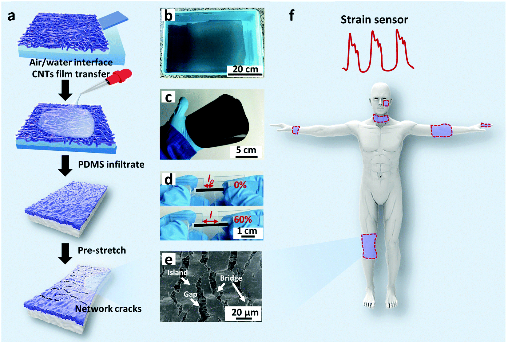 | ||
| Fig. 1 Illustration of the fabrication process of CNTs films/PDMS strain sensors. (a) Multilayer CNTs films obtained by repeat transfer of single layer CNTs film and infiltrated by PDMS to prepare CNTs films/PDMS composite and network cracks appeared after pre-stretching. (b) Large area free-standing CNTs film on air/water interface. (c) CNTs films/PDMS composite after diluted PDMS solution infiltration and curing. (d) Photograph of the cut sample of CNTs films/PDMS composite attached on a home-made fixing device. The strain sensor before (top) and after (bottom) being stretched by 60%. Here, l0 and l are the length of the strain sensor before and after stretching by 60%, respectively. (e) Top view scanning electron microscope (SEM) image showing the prepared network cracks after pre-stretching, consisting of gaps, islands, and bridges connecting separated islands. (f) Illustration of strain sensor used in different parts of human body for the detection of human motion. | ||
By controlling the repeat transfer times of CNTs films, different layers of CNTs films (1, 5, 10, and 15 layers (L)) were easily prepared. The optical transmittance gradually decreases with an increase in the layer number of CNTs films (Fig. S2a, ESI†). The top view of SEM image of the CNTs films shows porous structure (inset of Fig. 2a), thus facilitating the PDMS solution infiltration. The top view of SEM image after PDMS infiltration shows a relative smooth surface, indicating that PDMS solution infiltrated through the entire depth of the CNTs films and most CNTs were embedded in PDMS with few pieces of CNTs exposed to air, which facilitated the electrical wiring process (Fig. 2a). The cross-sectional SEM image shows bilayer structures, consisting of a conductive layer at the top (CNTs films/PDMS) and an elastic polymer layer at the bottom (pure PDMS) (Fig. 2b). Upon stretching, the homogeneous fractures appeared in the multilayer CNTs films/PDMS composite and network cracks were formed (Fig. 2c). It can be clearly seen that the network cracks are connected with separated islands and bridges (Fig. 2d).
 | ||
| Fig. 2 SEM results of the fabrication process. (a) Top view SEM image of the CNTs films/PDMS composite. Inset: Top view SEM image of multilayer CNTs films, scale bar: 1 μm. (b) Cross-sectional SEM image of the CNTs films/PDMS strain sensor, showing the top conductive layer (CNTs films/PDMS) and bottom elastic layer (PDMS). (c) SEM image showing the network cracks, reflecting the homogeneous fracturing of CNTs films/PDMS composite. (d) The arrows indicating the island width. | ||
The cross-sectional SEM image of CNTs films (Fig. S3a, top row, ESI†) clearly shows the thickness of a single layer of CNTs film to be about 386 nm. The theoretical thickness of multilayer CNTs films can be easily calculated (Fig. S4, top black line, ESI†). However, the practical thickness (Fig. S4, middle black line, ESI†) is smaller than the theoretical value, possibly due to the densification of porous layer structures in the drying process. This endows the CNTs films/PDMS conductive layer more brittleness, which is beneficial for the formation of cracks. Due to the stiffness mismatch between the top conductive layer and bottom elastic polymer layer, network cracks perpendicular to strain loading direction were produced after pre-stretching (multilayer CNTs films/PDMS samples). The thickness-dependent morphologies of CNTs films/PDMS strain sensors are shown in Fig. 3. There are no cracks in the 1-layer sample, while network cracks are observed for samples with more than 5 layers. The cracks pass partially through the width of the sample, so the conductive pathways could not be totally disconnected by one single crack, which is important for the large workable strain range of the as-fabricated sensors. Specifically, network cracks consisting of gaps, islands, and bridges connecting separated islands were created after pre-stretching as shown in Fig. 1e. With an increase in thickness of CNTs film, it is evident that the size of the island between the gaps became larger from 11 μm (5 layers) to 41 μm (15 layers) (Fig. S4, bottom red line, ESI†), reflecting that the crack density changed from dense to loose macroscopically.
 | ||
| Fig. 3 Optical images (transmission mode) of the thickness dependent crack morphologies of CNTs films/PDMS strain sensors by transferring (a) 1 layer of CNTs film, (b) 5 layers of CNTs films, (c) 10 layers of CNTs films, (d) 15 layers of CNTs films. | ||
Performance of multilayer CNTs films/PDMS strain sensors
The electromechanical characteristics of the CNTs films/PDMS strain sensors were investigated (Fig. 4a). The strain sensors with 15 layers of CNTs films responded to the applied strain with two stage GF behaviors. In the first stage (0 < ε < 40%), there is a sharp increase in relative resistance with maximum GF of 87. In the second stage (40 < ε < 100%), a relatively slow and almost linear increase of relative resistance appeared with GF of 6. It was reported that nonlinear response can lead to signal distortion45 and a in previous report, the as-fabricated strain sensors-based percolation networks rarely showed good linearity.46 Hence, it is worth noting that the present CNTs films/PDMS strain sensors show good linearity in the early part of first GF stage and entire part of second GF stage, which is beneficial for accurate sensing. The layer number of CNTs films has an important effect on the resistance behavior (Fig. S6, ESI†). The relative resistance behaviors can be ascribed to the thickness-dependent crack morphologies of CNTs films and their corresponding current flow pathways are schematically shown in Fig. S7 (ESI†). For samples with more than 10 layers of CNTs films (Fig. S7(iii), ESI†), there are fewer conductive pathways due to the relatively long cracks in the sample, thus resulting in a sharp decrease in the beginning. In the second GF stage, most cracks were open and no new cracks were formed, which led to a relatively slow decrease in the electrical conductivity. Although cracks were found in the composite film with 5 layers of CNTs films (Fig. S7(ii), ESI†), the network cracks were not able to cut off the electrical conduction pathways effectively due to the short crack length; hence, the sensitivity is lower. The relative change in resistance of samples with 1 layer of CNTs film (Fig. S7(i), ESI†) can be explained by reorientation of embedded CNTs within the PDMS matrix.26 The capability of adjusting GF would meet the demand of tunable sensitivities for various strain sensor applications. | ||
| Fig. 4 Electromechanical properties of the CNTs films/PDMS strain sensors. (a) The relative change in resistance versus strain curves of 15 layers of CNTs films/PDMS strain sensors, showing two stage GF behaviours. (b) The relative resistance changes under different strains (5%, 10%, 20%, and 40%) for five cycles. (c) The relative resistance changes versus strain curves in the small strain region (up to 1.5% strain). Inset: The time-relative resistance change curve for ten stretching/releasing cycles with strain of 0.007%, showing the minimum detection limit of 0.007% strain (with 1% pre-stretch). (d) Relative resistance change of the strain sensor with repeated cycles (1500 cycles) of stretching and releasing of 20% strain. (e) Relative resistance change to bending deformation, leading to extension (outward bending) and compression (inward bending) of the sensor. (f) Relative resistance changes of the sensor during cyclic outward and inward bending tests. | ||
The relative resistance increased as the strain increased under cyclic stretching–releasing of 5, 10, 20, and 40% strain (Fig. 4b). Stable and identical responses could be obtained, thus indicating the high reliability of the sensors. The sharp overshoots at each strain can be attributed to the viscoelasticity of the PDMS composite. In small strain sensing range, the strain sensors can be employed to sense strain less than 1.5% (Fig. 4c). The inset of Fig. 4c shows the time-dependent resistance curve of the stretching/releasing cycles with strain of 0.007% (with 1% pre-stretch), demonstrating particularly remarkable ability to detect ultralow strain of 0.007%. It is noteworthy that there are two advantages of using the strain sensor with 1% pre-stretch. One advantage is that the sensitivity can be tuned to the maximum value in the working strain range to improve the detection limit of the sensor. The other advantage is that the monitored signals will be more stable due to effective transfer of exerted strain to sensors. The long term cycling stability of the strain sensor was also tested (Fig. 4d). There was no substantial change in the relative resistance with 1500 stretching cycles under 20% uniaxial strain, suggesting that the strain sensor possesses excellent durability and reliability. Kang et al.41 reported that the performance of the zip-like nanoscale crack junctions remains unchanged up to about 500 loading and unloading cycles under 0–2% strain. The mechanical durability test in present study shows that the as-fabricated strain sensor has good repeatability and stability up to 1000 cycles under 20% strain. (Fig. S8, ESI†). Resistance hysteresis during the stretching/releasing can be attributed to the viscoelasticity of the PDMS (Fig. S9a, ESI†). The strain sensor exhibits fast response time of 65 ms when the quasi-instantaneous stimuli were applied (Fig. S9b, ESI†). In addition, the strain sensor with high sensitivity can usually detect only pulse signal accurately,41 while the strain sensor with wide sensing range can be used only for large strain detection like finger bending.19 The strain sensor fabricated in the present study has the ability to detect both subtle and large strain excellently (Table S1, ESI†).
In addition to stretching, the relative change in resistance of sensors during bending was also investigated. The bending setup is shown in Fig. S2e and f (ESI†). The sensor was fixed on a paper substrate. The stepper was propelled on one end of the paper substrate with the other end fixed for cyclic bending test. The bending angle θ was defined as the external angle of the two ends. The relative resistance increased significantly with outward bending and decreased tardily with inward bending. For example, the relative resistance change is 0.4 for outward bending, while it is 0.1 for inward bending under the same bending angle of 30° (Fig. 4e). The outward bending widens the gap between islands, resulting in an increase in resistance. In case of inward bending, the crack morphology did not significantly changed for those cracks in close contact and thus, the resistance decreased slightly. The strain sensor shows reversible response under both outward and inward bending (Fig. 4f).
Sensing mechanism of multilayer CNTs films/PDMS strain sensors
In order to understand the working mechanism of the network cracks based strain sensor, the deformation of CNTs films/PDMS composite under different strains was investigated (Fig. 5a). It is worth noting that the network cracks were produced during the pre-stretching process and no new gaps and islands were formed during subsequent stretching. Fig. 5a shows that there were no opening cracks at the initial state. The number of cracks significantly increased with further increase in strain (to 20%) and then changed slightly under subsequent loading. The gap between cracks increased monotonically during the strain loading process (Fig. 5c). Although most cracks opened at 60% strain, bridges between the disconnected networks prevented rupturing of the conductive pathways under large deformation; this is important for the large workable strain range. The change of crack morphology can be vividly simulated by Chinese paper cuttings (Fig. 5b). To quantitatively understand the two stage GF behavior of relative resistance change, a simplified resistance model based on evolution of the network cracks morphology is shown in Fig. 5d. | (1) |
 | ||
| Fig. 5 Strain sensing mechanism of CNTs films/PDMS strain sensors. (a) Series of optical images (transmission mode) of the CNTs films/PDMS composite (10 layers) being stretched from 0% to 60%. (b) Chinese paper cuttings simulating the change of crack morphology from unstrained to strained states. (c) Average gap width versus strain loading. (d) The resistance model of a sensing unit. | ||
Sensing applications of multilayer CNTs films/PDMS strain sensors
The excellent sensitivity and large strain range of the CNTs films/PDMS strain sensor make them suitable for potential applications in various fields. Fig. 6a shows the resistance change caused by a hair strand at two different pressures: 55 Pa and 114 Pa. The two end sides of the strain sensor were fixed firmly on a homemade device. Then, the sensor in the straight state changed into the bent state when touched with the hair strand and the length increased, leading to the increase in resistance. The air blow produced by ear syringe ball can also be detected, showing the non-contact stimuli detection ability of our sensor (Fig. 6b). When the sensor was attached to the speaker of an iPhone, musical vibration can be detected in real time (Fig. 6c). Temporal and static signals were produced by touching the sensor with a finger (Fig. 6d). The produced short and long signals correspond to “dots” and “dashes” in Morse code, representing the signals of “CAS”. | ||
| Fig. 6 Small strain sensing applications of the proposed strain sensor. (a) Relative resistance change with touch using a hair with two different pressures: 55 Pa and 114 Pa. (b) Signals of air blow produced by ear syringe ball with two different pressures: 114 Pa and 221 Pa. (c) Relative resistance change caused by music vibration of iPhone. (d) Temporal and static signals produced by pressing the sensor with a finger, representing the signals of “CAS” in Morse code. | ||
As for subtle strain detection of human motion, Fig. 7a shows a sensor attached to a wrist band to detect the pulse signal of the radial artery. The data were collected under two different conditions, normal and after 20 push-ups (Fig. 7b). Under normal conditions, 0.8 s of one pulse can be calculated from the stable arterial pulse waveforms and the corresponding heart rate is 75 beats min−1, which is within normal heartbeat range of a healthy person. The magnified view of wrist pulse signals is shown in Fig. 7c. It can be seen that the signal intensity after the push-ups activity increased and the figure clearly reveals the characteristic peaks including those attributed to percussion (P), tidal (T), and diastolic (D) waves of arterial pulses. Since artery pulse as well as heart rate are vital health-related indexes, the strain sensor can be used as a promising wearable diagnostic device to provide detailed clinical information by long-term monitoring of these parameters. The laryngeal prominence movement can also be monitored by attaching the strain sensor onto the throat of a volunteer (Fig. 7d). The repetitive signal patterns were obtained when the volunteer spoke several words such as “hello”, “strain sensor”, and “film”, showing its potential applications in voice recognition and human/machine interface (Fig. 7e). Other throat movements such as swallowing and coughing can also be detected (Fig. 7f).
 | ||
| Fig. 7 Subtle strain detection of human motion. (a) Optical image of the sensor attached on wrist. (b) The relative resistance changes of the sensor in response to the pulse of radial artery from the wrist. (c) Close up of the corresponding region in b. (d) Optical image showing the sensor attached on laryngeal prominence. (e) Relative resistance change caused by laryngeal prominence movement for phonetic recognition. (f) Relative resistance change caused by swallows and coughs. | ||
As for large strain detection of human motion, the sensor was attached on the joints of the body. Fig. 8a shows the relative resistance change with wrist bending. Fig. 8b shows the relative resistance change caused by the bending of the index finger. When the finger bent to a certain angle, the relative resistance of the strain sensor rapidly reached a certain value. Larger bending angle would lead to larger increase in the relative resistance. When the finger moved back to its original position, the relative resistance recovered.
 | ||
| Fig. 8 Large strain detection of human motion. Relative resistance change caused by (a) wrist bending, (b) finger bending with different angles, respectively, (c) elbow joint bending and (d) knee joint bending. | ||
Fig. 8c and d show the relative resistance change with elbow joint bending and knee joint bending, respectively.
Conclusions
In conclusion, we developed a highly stretchable and sensitive strain sensor with multilayer free-standing CNTs films infiltrated by PDMS solution. The hierarchical multilayer CNTs films with controlled thickness tend to form the cracks in the network structure in the form of gaps, islands, and bridges connecting separated islands in CNTs films/PDMS composite, which leads to the achievement of the higher GF (87) than the values obtained in previous reports. The high GF significantly amplifies the sensing signals of the strain sensors. The macroscopic area of CNTs films/PDMS composite provides an easy way to achieve the scalable fabrication of highly stable strain sensors. The as-fabricated strain sensors were employed in practical application for the full range detection of human motions such as that of artery pulses, laryngeal prominence, finger bending and wrist bending.Conflicts of interest
There are no conflicts to declare.Acknowledgements
We thank the Natural Science Foundation of China (51573203, 51473179), the Bureau of International Cooperation of Chinese Academy of Sciences (174433KYSB20170061), the Bureau of Frontier Science and Education of Chinese Academy of Sciences (QYZDB-SSW-SLH036), Fujian province- Chinese Academy of Sciences STS project (2017T31010024), Ningbo Science and Technology Bureau (2015C110031), and Youth Innovation Promotion Association of Chinese Academy of Science (2016268 and 2017337). Open Access funding provided by the Max Planck Society.Notes and references
- W. Gao, S. Emaminejad, H. Y. Y. Nyein, S. Challa, K. Chen, A. Peck, H. M. Fahad, H. Ota, H. Shiraki, D. Kiriya, D.-H. Lien, G. A. Brooks, R. W. Davis and A. Javey, Nature, 2016, 529, 509 Search PubMed.
- T. Q. Trung and N. E. Lee, Adv. Mater., 2016, 28, 4338 Search PubMed.
- K. Takei, W. Honda, S. Harada, T. Arie and S. Akita, Adv. Healthcare Mater., 2015, 4, 487 Search PubMed.
- M. A. McEvoy and N. Correll, Science, 2015, 347, 1261689 Search PubMed.
- S. Lim, D. Son, J. Kim, Y. B. Lee, J. K. Song, S. Choi, D. J. Lee, J. H. Kim, M. Lee, T. Hyeon and D.-H. Kim, Adv. Funct. Mater., 2015, 25, 375 Search PubMed.
- J. Lee, H. Kwon, J. Seo, S. Shin, J. H. Koo, C. Pang, S. Son, J. H. Kim, Y. H. Jang, D. E. Kim and T. Lee, Adv. Mater., 2015, 27, 2433 Search PubMed.
- J. W. Jeong, W. H. Yeo, A. Akhtar, J. J. S. Norton, Y. J. Kwack, S. Li, S. Y. Jung, Y. Su, W. Lee, J. Xia, H. Cheng, Y. Huang, W.-S. Choi, T. Bretl and J. A. Rogers, Adv. Mater., 2013, 25, 6839 Search PubMed.
- A. A. Barlian, W.-T. Park, J. R. Mallon, A. J. Rastegar and B. L. Pruitt, Proc. IEEE, 2009, 97, 513 Search PubMed.
- Q. Li, Z. Ullah, W. Li, Y. Guo, J. Xu, R. Wang, Q. Zeng, M. Chen, C. Liu and L. Liu, Small, 2016, 12, 5058 Search PubMed.
- I. You, B. Kim, J. Park, K. Koh, S. Shin, S. Jung and U. Jeong, Adv. Mater., 2016, 28, 6359 Search PubMed.
- H. Schlicke, M. Rebber, S. Kunze and T. Vossmeyer, Nanoscale, 2016, 8, 183 Search PubMed.
- J. Lee, S. Kim, J. Lee, D. Yang, B. C. Park, S. Ryu and I. Park, Nanoscale, 2014, 6, 11932 RSC.
- M. Segev-Bar and H. Haick, ACS Nano, 2013, 7, 8366 CrossRef CAS PubMed.
- N. Lu, C. Lu, S. Yang and J. Rogers, Adv. Funct. Mater., 2012, 22, 4044 CrossRef CAS.
- T. Yamada, Y. Hayamizu, Y. Yamamoto, Y. Yomogida, A. Izadi-Najafabadi, D. N. Futaba and K. Hata, Nat. Nanotechnol., 2011, 6, 296 CrossRef CAS PubMed.
- D. J. Lipomi, M. Vosgueritchian, B. C. K. Tee, S. L. Hellstrom, J. A. Lee, C. H. Fox and Z. Bao, Nat. Nanotechnol., 2011, 6, 788 CrossRef CAS PubMed.
- H. Zhu, X. Wang, J. Liang, H. Lv, H. Tong, L. Ma, Y. Hu, G. Zhu, T. Zhang, Z. Tie, Z. Liu, Q. Li, L. Chen, J. Liu and Z. Jin, Adv. Funct. Mater., 2017, 27, 1606604 CrossRef.
- K. Suzuki, K. Yataka, Y. Okumiya, S. Sakakibara, K. Sako, H. Mimura and Y. Inoue, ACS Sens., 2016, 1, 817 CrossRef CAS.
- S. J. Park, J. Kim, M. Chu and M. Khine, Adv. Mater. Technol., 2016, 1, 1600053 CrossRef.
- E. Roh, B.-U. Hwang, D. Kim, B.-Y. Kim and N.-E. Lee, ACS Nano, 2015, 9, 6252 CrossRef CAS PubMed.
- C. Li, Y.-L. Cui, G.-L. Tian, Y. Shu, X.-F. Wang, H. Tian, Y. Yang, F. Wei and T.-L. Ren, Sci. Rep., 2015, 5, 15554 CrossRef CAS PubMed.
- H.-S. Liu, B.-C. Pan and G.-S. Liou, Nanoscale, 2017, 9, 2633 RSC.
- B. S. Kim, J. B. Pyo, J. G. Son, G. Zi, S.-S. Lee, J. H. Park and J. Lee, ACS Appl. Mater. Interfaces, 2017, 9, 10865 CAS.
- S. Gong, D. T. H. Lai, Y. Wang, L. W. Yap, K. J. Si, Q. Shi, N. N. Jason, T. Sridhar, H. Uddin and W. Cheng, ACS Appl. Mater. Interfaces, 2015, 7, 19700 CAS.
- S. Gong, D. T. H. Lai, B. Su, K. J. Si, Z. Ma, L. W. Yap, P. Guo and W. Cheng, Adv. Electron. Mater., 2015, 1, 1400063 CrossRef.
- M. Amjadi, A. Pichitpajongkit, S. Lee, S. Ryu and I. Park, ACS Nano, 2014, 8, 5154 CrossRef CAS PubMed.
- D.-Y. Wang, L.-Q. Tao, Y. Liu, T.-Y. Zhang, Y. Pang, Q. Wang, S. Jiang, Y. Yang and T.-L. Ren, Nanoscale, 2016, 8, 20090 RSC.
- X. Li, T. Yang, Y. Yang, J. Zhu, L. Li, F. E. Alam, X. Li, K. Wang, H. Cheng, C. T. Lin, Y. Fang and H. Zhu, Adv. Funct. Mater., 2016, 26, 1322 CrossRef CAS.
- R. Xu, Y. Lu, C. Jiang, J. Chen, P. Mao, G. Gao, L. Zhang and S. Wu, ACS Appl. Mater. Interfaces, 2014, 6, 13455 CAS.
- C. S. Boland, U. Khan, G. Ryan, S. Barwich, R. Charifou, A. Harvey, C. Backes, Z. Li, M. S. Ferreira, M. E. Mobius, R. J. Young and J. N. Coleman, Science, 2016, 354, 1257 CrossRef CAS PubMed.
- Y. Li, Y. A. Samad and K. Liao, J. Mater. Chem. A, 2015, 3, 2181 CAS.
- Y. A. Samad, Y. Li, S. M. Alhassan and K. Liao, ACS Appl. Mater. Interfaces, 2015, 7, 9195 CAS.
- F. Han, J. Li, S. Zhao, Y. Zhang, W. Huang, G. Zhang, R. Sun and C. P. Wong, J. Mater. Chem. C, 2017, 5, 10167 RSC.
- S. Zhao, L. Guo, J. Li, N. Li, G. Zhang, Y. Gao, J. Li, D. Cao, W. Wang, Y. Jin, R. Sun and C.-P. Wong, Small, 2017, 13, 1700944 CrossRef PubMed.
- X. Liao, Z. Zhang, Z. Kang, F. Gao, Q. Liao and Y. Zhang, Mater. Horiz., 2017, 4, 502 RSC.
- C. Wang, X. Li, E. Gao, M. Jian, K. Xia, Q. Wang, Z. Xu, T. Ren and Y. Zhang, Adv. Mater., 2016, 28, 6640 CrossRef CAS PubMed.
- M. Amjadi, M. Turan, C. P. Clementson and M. Sitti, ACS Appl. Mater. Interfaces, 2016, 8, 5618 CAS.
- M. Amjadi, K. U. Kyung, I. Park and M. Sitti, Adv. Funct. Mater., 2016, 26, 1678 CrossRef CAS.
- Y. R. Jeong, H. Park, S. W. Jin, S. Y. Hong, S. S. Lee and J. S. Ha, Adv. Funct. Mater., 2015, 25, 4228 CrossRef CAS.
- I. M. Graz, D. P. J. Cotton and S. P. Lacour, Appl. Phys. Lett., 2009, 94, 071902 CrossRef.
- D. Kang, P. V. Pikhitsa, Y. W. Choi, C. Lee, S. S. Shin, L. Piao, B. Park, K.-Y. Suh, T.-i. Kim and M. Choi, Nature, 2014, 516, 222 CrossRef CAS PubMed.
- Q. Liu, J. Chen, Y. Li and G. Shi, ACS Nano, 2016, 10, 7901 CrossRef CAS PubMed.
- Y. Cai, J. Shen, Z. Dai, X. Zang, Q. Dong, G. Guan, L. J. Li, W. Huang and X. Dong, Adv. Mater., 2017, 29, 1606411 CrossRef PubMed.
- P. Xiao, J. Gu, C. Wan, S. Wang, J. He, J. Zhang, Y. Huang, S.-W. Kuo and T. Chen, Chem. Mater., 2016, 28, 7125 CrossRef CAS.
- N. Luo, W. Dai, C. Li, Z. Zhou, L. Lu, C. C. Y. Poon, S.-C. Chen, Y. Zhang and N. Zhao, Adv. Funct. Mater., 2016, 26, 1178–1187 CrossRef CAS.
- R. Wang, N. Jiang, J. Su, Q. Yin, Y. Zhang, Z. Liu, H. Lin, F. A. Moura, N. Yuan, S. Roth, R. S. Rome, R. Ovalle-Robles, K. Inoue, S. Yin, S. Fang, W. Wang, J. Ding, L. Shi, R. H. Baughman and Z. Liu, Adv. Funct. Mater., 2017, 27, 1702134 CrossRef.
Footnote |
| † Electronic supplementary information (ESI) available. See DOI: 10.1039/c8tc00433a |
| This journal is © The Royal Society of Chemistry 2018 |