
 Open Access Article
 This Open Access Article is licensed under a
 Creative Commons Attribution 3.0 Unported Licence
Photocatalytic and electrically conductive transparent Cl-doped ZnO thin films via aerosol-assisted chemical vapour deposition†
Arreerat
Jiamprasertboon
ab,
Michael J.
Powell
 b,
Sebastian C.
Dixon
b,
Raul
Quesada-Cabrera
b,
Abdullah M.
Alotaibi
b,
Yao
Lu
c,
Aoyun
Zhuang
b,
Sanjayan
Sathasivam
b,
Theeranun
Siritanon
a,
Ivan P.
Parkin
b and
Claire J.
Carmalt
*b
b,
Sebastian C.
Dixon
b,
Raul
Quesada-Cabrera
b,
Abdullah M.
Alotaibi
b,
Yao
Lu
c,
Aoyun
Zhuang
b,
Sanjayan
Sathasivam
b,
Theeranun
Siritanon
a,
Ivan P.
Parkin
b and
Claire J.
Carmalt
*b
aSchool of Chemistry, Institute of Science, Suranaree University of Technology, 111 University Avenue, Muang, Nakhon Ratchasima, 30000, Thailand. E-mail: c.j.carmalt@ucl.ac.uk
bMaterial Chemistry Centre, Department of Chemistry, University College London, 20 Gordon Street, London, WC1H 0AJ, UK
cDepartment of Mechanical Engineering, University College London, London, WC1E 7JE, UK
First published on 12th June 2018
Abstract
A simple, economical and effective solution-based chemical vapour deposition (CVD) technique, aerosol-assisted CVD, has been successfully applied to produce inexpensive Cl-doped ZnO films using Zn acetate dihydrate and FeCl3. X-ray photoelectron spectroscopy and the increase in cell parameters from powder X-ray diffraction determined that Cl had been doped into the wurtzite ZnO lattice. The Cl-doping had a significant effect on the morphology of the thin films synthesised and resulted in an improvement in the visible light transmission and lower electrical resistance (typical resistivities of doped films ∼10−2 Ω cm). The highest transmittance (% T) of 85% was obtained when 7 mol% FeCl3 was used in the precursor solution and the lowest resistivity of 4.28 ± 0.41 × 10⁻² Ω cm was obtained with 5 mol% FeCl3. The greatest photocatalytic activity of stearic acid degradation under UVA irradiation was obtained on using 10 mol% FeCl3, resulting in the highest formal quantum efficiency (FQE) of 3.0 ± 0.1 × 10⁻⁴ molecule per photon. These films, therefore, display transparent conducting oxide and photocatalytic properties, giving multifunctional characteristics and promising applications.
Introduction
Transparent conducting oxide (TCO) materials have the unique coexistent properties of high optical transparency and high electrical conductivity that contribute to various electronic devices such as liquid crystal displays (LCDs), touch panel screens, E-paper, defrosting windows, electrochromic windows and mirrors, photovoltaics, flexible electronics and invisible security circuits.1,2 Semiconducting oxides with large band gap energies (>3.1 eV) and the ability to be doped to generate low resistivity (<10−2 Ω cm) are required for TCO properties.3 Even though Sn-doped In2O3 (ITO) and F-doped SnO2 (FTO) are the most widely used TCOs because of their excellent properties of low electrical resistivity with high transparency,1,4–6 In2O3 has the disadvantages of high cost of extraction and processing, as well as concern over the relative scarcity of indium ores. Sn also has also suffers from price fluctuations compared to other elements, such as Zn.7Zinc oxide (ZnO) is a promising candidate for TCOs because it is well known as an intrinsic n-type semiconductor with a wide band gap of ca. 3.37 eV; moreover, it has high thermal stability,8 is inexpensive, earth abundant and relatively nontoxic compared to ITO and FTO.8–12 Doping is a strategy to enhance the electrical conductivity of TCO materials. Cation dopants such as Al3+, Ga3+, In3+,13–19 Sc3+,20 Si4+ (ref. 21 and 22) and Cu23 and anion dopants such as F−,16,24,25 Cl− (ref. 26) and N3−,27 have all been successfully incorporated into ZnO thin films. Anion doping is considered to be a superior route to obtain high carrier concentration and mobility while maintaining high transparency, because the conduction band (CB) is less perturbed by the dopant and thus the scattering of electrons in the CB is minimized.1 F-Doping has been extensively studied and the resulting materials show excellent properties,5,28,29 investigations on the use of other anions, such as Cl, are relatively limited. However, there have been some reports on the electrical, optical and photoelectrochemical properties of Cl-doped ZnO, which show the potential of Cl doping.30–35 Therefore, we were interested in exploring further the novel properties of ZnO:Cl, in particular the film deposition method which has been shown to play a key role in modifying the film properties. Aerosol-assisted chemical vapour deposition (AACVD) is an effective technique to control the morphology and simultaneously the properties of the deposited films.36 Moreover, it is a simple, sustainable and scalable deposition film fabrication technique37 that allows for the use of a variety of precursors with appropriate solubility in a suitable solvent.12 In the procedure, soluble halide precursors can be utilised which are generally cheaper than metal–organic precursors.38
In general, TCO films have poor photocatalytic activity and photocatalytic films show poor TCO properties.39 For example, W-doped TiO2 and Nb-doped TiO2 films are good photocatalysts and electrically conductive (resistivities were 6.3 × 10⁻¹ to 6.3 × 10⁻² Ω cm and 5.8 × 10⁻² to 1.3 × 10⁻³ Ω cm, respectively) but they are coloured;40,41 P-doped TiO2 films are also good photocatalysts but their conductivity (resistivities were 1.69–6.49 Ω cm) as well as transparency (% T is less than 80%) have not yet passed the requirement to be considered good TCO materials.42 In general, multifunctional properties are not commonly observed in most films. The ability to synthesize films that display both good electrical and photocatalytic properties whilst being transmissive of visible wavelengths would therefore be of benefit for multifunctional devices.
Here, the Cl-doped ZnO films were prepared by a simple, economical and potential film deposition, AACVD technique for the first time. Photocatalytic properties of ZnO:Cl films are first observed. Photocatalytic transparent conducting Cl-doped ZnO thin films are described as promising materials for sustainable applications.
Experimental
Film synthesis
All films were synthesised via aerosol assisted chemical vapor deposition (AACVD). Zn(II) acetate dihydrate, Zn(OAc)2·2H2O, (≥98%, Sigma-Aldrich) and ferric chloride anhydrous, FeCl3, (98%, Aldrich) were used as the Zn and Cl precursors respectively. All precursors were used as received without further purification. Methanol (99.9%, Fisher Scientific) was used as the solvent. Nitrogen gas (99.99%, BOC) was used as the carrier gas.In a typical deposition, the precursor solution was prepared by dissolving Zn(OAc)2·2H2O (0.50 g, 2.28 mmol) in methanol (20 mL). FeCl3 was dissolved in methanol and then added to the zinc acetate solution in the corresponding mol% of 0, 1, 3, 5, 7, 10 and 15. Each precursor was stirred until separately for ca. 5 minutes and then mixed by stirring to give the final precursor solution. A glass substrate, coated with a 50 nm SiO2 barrier layer (NSG Pilkington Ltd), with the dimension of 3.2 mm × 45 mm × 100 mm was used. The SiO2 barrier layer is important to prevent leeching of ions between the substrate and the film. Prior to depositing, the substrate was cleaned by detergent, isopropanol and acetone, respectively. The AACVD apparatus is illustrated in Fig. 1. The substrate was placed on a carbon heating block, which was enclosed in a quartz tube. The top plate of stainless steel of 4.8 cm × 15 cm was suspended over the substrate approximately 8 mm to assist the laminar flow of the aerosol. In the deposition, the obtained precursor solution was atomised using a ‘Liquifog’ piezo ultrasonic humidifiers (Johnson Matthey). The aerosol or mist was generated and transported to the heated substrate through the baffle via nitrogen carrier gas with a flow rate of 1.5 L min−1. The deposition temperature was 500 °C for all samples. A typical deposition would take 15–20 minutes in order for all of the solution to aerosolize, after which the substrate was left to cool under a continuous flow of nitrogen gas and removed when the temperature of reactor was below 100 °C. The film was cut into pieces of 1 × 1 cm2 prior to the characterisations.
 | ||
| Fig. 1 The schematic illustration of aerosol assisted chemical vapour deposition (AACVD) apparatus. | ||
Film characterisation
X-ray photoelectron spectroscopy (XPS) spectra of Zn 2p, Fe 2p, Cl 2p and O 1s were investigated to confirm the oxidation states as well as compositions of constituent elements. A Thermo Scientific K-alpha spectrometer with a monochromatic Al Kα radiation, a dual beam charge compensation system and constant pass energy of 50 eV were utilised. The collected spectra were fitted using CasaXPS software. The C 1s peaks at 284.5 eV were used as reference for binding energy calibration. X-ray diffraction (XRD) measurement, using a Bruker-Axs D8 X-ray diffractometer with parallel beam optics equipped with a PSD LynxEye silicon strip detector, was performed to check the phase purity of the films. Monochromatic Cu Kα1 and Kα2 X-rays (λ = 1.54056 Å and 1.54439 Å, respectively), with the intensity ratio of 2![[thin space (1/6-em)]](https://www.rsc.org/images/entities/char_2009.gif) :1, were generated using a voltage of 40 kV and a current of 40 mA. The incident beam angle was kept at a grazing setup of 1°. XRD patterns were collected with 2θ range of 10–66° with a step size of 0.05° by a scan rate of 4 s per step. Le Bail refinement using GSAS and EXPGUI software43,44 was done to get the cell parameters. Scanning electron microscope (SEM) images and side-on SEM images were gained to study the surface morphology and film thickness, respectively, using a JEOL JSM-6301F Field Emission instrument with an operated acceleration voltage of 10 kV. UV/vis transmittance spectra were measured to obtain the optical properties by using a Perkin Elmer Lambda 950 UV/vis/NIR Spectrophotometer. Surface topology and roughness (root mean squared, Rq) were characterised using an atomic force microscope (AFM, Bruker Multimode 8). The tips were used in the ScanAsyst tapping mode to scan the area of 1.0 μm × 1.0 μm, respectively, with 512 scans.
:1, were generated using a voltage of 40 kV and a current of 40 mA. The incident beam angle was kept at a grazing setup of 1°. XRD patterns were collected with 2θ range of 10–66° with a step size of 0.05° by a scan rate of 4 s per step. Le Bail refinement using GSAS and EXPGUI software43,44 was done to get the cell parameters. Scanning electron microscope (SEM) images and side-on SEM images were gained to study the surface morphology and film thickness, respectively, using a JEOL JSM-6301F Field Emission instrument with an operated acceleration voltage of 10 kV. UV/vis transmittance spectra were measured to obtain the optical properties by using a Perkin Elmer Lambda 950 UV/vis/NIR Spectrophotometer. Surface topology and roughness (root mean squared, Rq) were characterised using an atomic force microscope (AFM, Bruker Multimode 8). The tips were used in the ScanAsyst tapping mode to scan the area of 1.0 μm × 1.0 μm, respectively, with 512 scans.
Hall effect measurement with the van der Pauw method was carried out on an Ecopia HMS-3000 to investigate the electrical properties: resistivity (ρ), carrier concentration (n) and carrier mobility (μ). A magnetic field of 0.58 T and an input current of 1 μA to 1 mA were applied for the measurement.
To determine the photocatalytic properties, the test of stearic acid degradation was studied. A thin layer of stearic acid was coated on films by dipping in a 0.05 M stearic acid solution in chloroform using a bespoke dip coating apparatus, which withdraws the substrate at a fixed rate vertically from the stearic acid solution. Fourier transform infrared (FTIR) spectra were collected in the absorbance mode in the range of 2700–3000 cm−1, using a Perkin Elmer RX-I instrument, to monitor the C–H bond decomposition under UVA (λ = 365 nm) light exposure. A 2 × 8 W blacklight-bulb (BLB) UVA lamps (Vilber-Lourmat) with the irradiation of ∼0.5 mW cm−2, as measured by a UVX meter (UVP), were used in the test. The linear regression of the initial 30–40% degradation steps (zero-order kinetics) with a conversion factor (1 cm−1 ≈ 9.7 × 10¹⁵ molecule of stearic acid per cm2)45 was utilised to determine the photocatalytic activity rates as formal quantum efficiency (FQE) value.
Results and discussion
Film synthesis
In the synthesis, the precursors Zn(OAc)2·2H2O and FeCl3 were dissolved in methanol. At low concentrations (below 5 mol%) of FeCl3 the solution was clear and colourless. However, at higher concentrations (>5 mol% of FeCl3) some white colloid was observed in the mixed solution, which may result due to the formation of iron hydroxides or iron oxohydroxochlorido species. The undoped ZnO films deposited were typically darker in hue than the doped films. This was attributed to higher carbon contamination in the undoped films, which was confirmed by the presence of C 1s XPS spectra in the bulk of films. The prepared films become more transparent with increasing the amount of FeCl3. Fig. 2 shows a photograph of the most transparent films prepared using 7 mol% FeCl3 in the solution precursor (right) compared with bare glass (left). The 15 mol% FeCl3-loaded precursor solution resulted in the deposition of a hazy film and hence it was not further characterised for optical and electrical properties. | ||
| Fig. 2 Photograph of bare glass (left) and 7 mol% FeCl3 loaded ZnO film (right). | ||
All the films had good adhesion to the substrate, passing the Scotch tape test and steel scalpel scratch test. The films showed good stability after six months storage under ambient condition and they were stable to common solvents such as methanol, isopropanol, acetone and chloroform. All films were deposited at 500 °C, since this temperature resulted in films with the optimum appearance, good coverage and the best electrical properties, in comparison to films deposited at 400 °C and 550 °C.
Elemental analysis
The chemical components and their oxidation states were studied by X-ray photoelectron spectroscopy (XPS) which indicated that Cl-doped ZnO thin films had been deposited. XPS core level spectra for Zn 2p, Fe 2p, Cl 2p and O 1s were performed. No Fe was observed in any of the samples (both surface and depth profiling). It has been previously reported that Fe can substitute at the Zn site in ZnO films, which can be in the form of either Fe2+ [ref. 46–48] or Fe3+ [ref. 49–52] or mixed Fe2+/Fe3+.53,54 However, no Fe substitution was observed in these films deposited via AACVD. This could be a result of side reactions occurring in the solution, such as a ligand exchange, yielding iron acetate. Indeed, after some AACVD depositions, a red precipitate was observed in the bubbler which may be iron acetate as this is insoluble and has been described previously as a red solid if impure or mixed iron/zinc acetates (ESI†).55,56 Furthermore, this would result in Zn2+ and Cl− being present in higher concentrations in the precursor solution. However, other reactions are also possible, for example anhydrous FeCl3 undergoes hydrolysis to produce HCl and iron hydroxide and the presence of HCl could result in Cl-doping.Zn 2p and O 1s spectra of all films show similar features; therefore the Cl-doped ZnO films formed using 10 mol% FeCl3 has been chosen as a representative example and is shown in Fig. 3(a) and (b). The Zn 2p3/2 peak, observed at 1020.6 (±0.2) eV, was assigned to Zn2+–O bond (Fig. 2a).57,58 The O 1s spectrum (Fig. 3b) can be deconvoluted into two peaks; the peak at 529.5 (±0.2) eV, corresponds to O2− in the lattice and the peak at 531.4 (±0.2) eV can be attributed to oxygen vacancies or loosely bound oxygen species, such as adsorbed O2 and –OH. This oxygen is related to chemisorption on the surface and at the grain boundaries of the polycrystalline films.59–62 The Cl 2p XPS spectra of all the Cl-doped films are shown in Fig. 3c, indicating that Cl was introduced into the films. The Cl 2p3/2 peak at around 198.4 (±0.2) eV corresponds to Cl–Zn bond. All XPS values quoted correspond to those observed in the literature.30,32,33
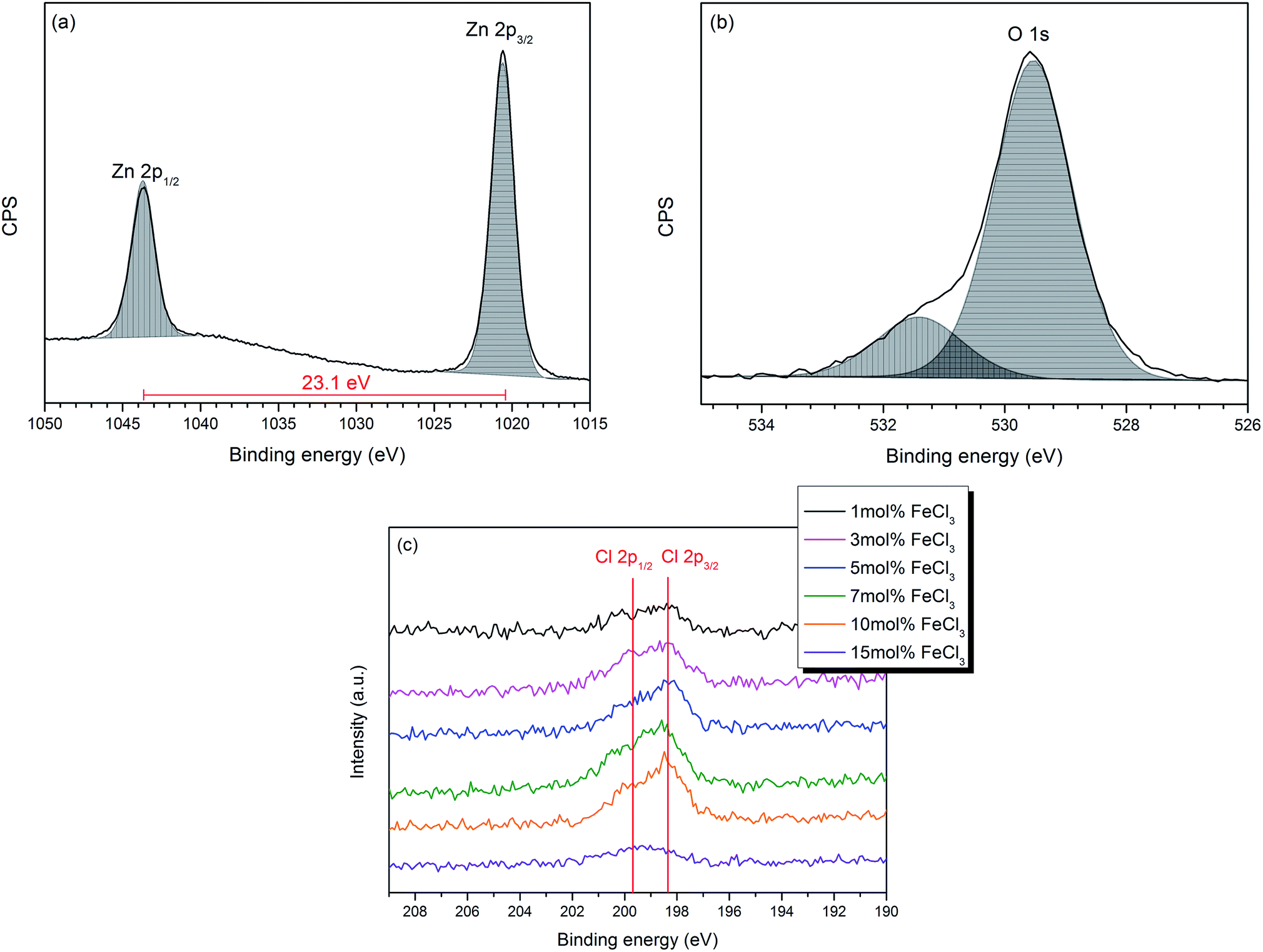 | ||
| Fig. 3 High-resolution XPS spectra of (a) Zn 2p3/2 (b) O 1s of the Cl-doped ZnO film formed from 10 mol% FeCl3 and (c) Cl 2p for all films. | ||
Although chlorine was detected within the XPS data, the signal was weak with a low signal to noise ratio, hence the at% of chlorine in all the Cl-doped samples was considered to be below 1 at%, as this is the threshold of reliable detection for XPS. Therefore, although chlorine can be detected and the influence of Cl can be seen in the change in preferential orientation and lattice parameters from the XRD data (vide infra), the measured values cannot be included as the error on these would be greater than the value calculated from the XPS data. Moreover, the calculated at% of Cl in the bulk by depth profile was lower than that at the surface and less than 1 at% (see ESI†). This suggests that the Cl concentration in the bulk was considerably lower due to preferential sputtering of Cl during the etching process, when Ar+ ion bombardment was performed, as it is a light element similar to F,16 O63 and S.64
Crystal structure
XRD patterns of all films (Fig. 4) can be indexed as the single phase of hexagonal wurtzite ZnO (space group: P63mc). The preferred orientation illustrates itself through differences in peak intensity from sample to sample. This generally occurs during the film growth in order to minimise the internal stress and surface energy.65 ZnO films have the preferred orientation of (002) plane along the c-axis which is normally observed in ZnO films as a result of film growth mechanism resulting in the most densely-packed and thermodynamically-favourable plane in the wurtzite structure.66 The preferred orientation changed to the (101) plane for the Cl-doped ZnO films formed using 1–5 mol% FeCl3 and then back to the (002) on increasing the amount of FeCl3 (7–15 mol%). It is worth noting that the (101) plane preferred orientation was observed in the case of Cl-doped ZnO films prepared by atomic layer deposition32 and Cl-doped ZnO nanospheres67 and microdisks,68 whereas the (002) plane was observed for Cl-doped ZnO nanodisks69 and nanowires.70 This suggests that the preparation methods and form of sample influences the preferred orientation. Cell parameters a, c and cell volume (Fig. 5), which were obtained from Le Bail refinement, increased from undoped to Cl-doped ZnO films. This is expected for incorporation of Cl into the ZnO structure, since a comparison of ionic radii indicates that O2− (ri = 1.40 Å) is substituted by the bigger anion Cl− (ri = 1.81 Å).71 | ||
| Fig. 4 XRD patterns of simulated bulk ZnO (ICSD #82028), undoped and Cl-doped ZnO thin films. All films can be indexed as the single phase of wurtzite ZnO. | ||
 | ||
| Fig. 5 Variation of cell parameters a, c and cell volume of the films with a change of mol% FeCl3 added to the precursor solution. The increase of cell parameters confirms the incorporation of Cl into the ZnO lattice. | ||
Surface morphology
SEM images (Fig. 6) illustrate that the morphology of the ZnO films can be affected by Cl doping. This can be rationalised from the preferred orientation change, which can be seen from XRD patterns (Fig. 4). The inclusion of Cl into the ZnO lattice had a significant effect on the surface morphology, such that even low levels of Cl in solution caused a change in the grain shape, as can be seen in the film formed using 5 mol% FeCl3. It was also observed that the average grain size increased with the increase of mol% FeCl3; this corresponds to the increase in crystallite size determined from Scherrer analysis (Table 1). The morphology present in the samples was different to Cl-doped ZnO films prepared via ALD, which was expected due to the effect of the different deposition techniques.32 However, the morphology changed to hexagonal for the film formed using 15 mol% FeCl3, this was also observed in ZnO thin films formed with acetic acid added to the precursor solution.72 Side-on SEM images (Fig. 6, inset) were used to gain the thickness of the films, which are given in Table 1. | ||
| Fig. 6 SEM images of ZnO and Cl-doped ZnO films with mol% FeCl3 loading of (a) 0 mol%, (b) 1 mol%, (c) 3 mol%, (d) 5 mol%, (e) 7 mol%, (f) 10 mol% and (g) 15 mol%. Side-on SEM (inset) shows film thickness. | ||
| Mol% FeCl3 | a (Å) | c (Å) | V (Å3) | Crystallite size (Å) | Thickness (nm) |
|---|---|---|---|---|---|
| 0 | 3.2506(11) | 5.2067(11) | 47.65(3) | 207.23 ± 0.25 | 930 |
| 1 | 3.2505(7) | 5.2091(12) | 47.67(3) | 297.07 ± 0.50 | 470 |
| 3 | 3.2511(4) | 5.2089(8) | 47.68(1) | 276.80 ± 3.82 | 450 |
| 5 | 3.2523(2) | 5.2119(5) | 47.74(1) | 328.83 ± 2.94 | 460 |
| 7 | 3.2536(4) | 5.2134(5) | 47.80(1) | 406.97 ± 7.71 | 570 |
| 10 | 3.2539(4) | 5.2152(4) | 47.82(1) | 377.27 ± 1.31 | 580 |
| 15 | 3.2553(2) | 5.2133(1) | 47.84(1) | 518.97 ± 4.14 | — |
Surface topology
AFM images (Fig. 7) show the topology of the films and give information about the film roughness, which is reported as the root mean squared (rms) roughness value. The undoped ZnO film had a rms of 12.9 ± 2.2 nm while the Cl-doped ZnO formed from 10 mol% FeCl3 had a similar rms of 15.4 ± 2.0 nm. Interestingly, the surface area difference of the undoped ZnO film and the Cl-doped ZnO formed from 10 mol% FeCl3 were not significantly different. | ||
| Fig. 7 AFM images of (a) undoped ZnO and (b) 10 mol% FeCl3 doped ZnO and 3D images of the same area (c) and (d). | ||
Functional properties
 | (1) |
The results of the photocatalytic testing are conveniently expressed in terms of formal quantum efficiency (ξ), which indicates the number of stearic acid molecules degraded per incident photon. It can be seen in Fig. 8 that the activity of the pure ZnO film was extremely poor whilst addition of small amounts of Cl precursor had a dramatic effect on photocatalytic performance. The best activities were recorded for the film deposited from 10 mol% FeCl3 with the highest ξ of 3.0 ± 0.1 × 10⁻⁴ molecule per photon, which was about 18 times greater than that of undoped ZnO film.
 | ||
| Fig. 8 The formal quantum efficiency (FQE) for the degradation of stearic acid on undoped and Cl-doped ZnO films under UVA illumination. Pilkington Activ glass is used as reference. All ZnO:Cl films are photocatalytically active and 10 mol% FeCl3 added show the best efficiency. | ||
The improved photocatalytic efficiency of Cl doped ZnO thin films compared with undoped ZnO thin films were likely due to changes in morphology, as shown in the SEM images (Fig. 6). Morphology is reported to be one of the most important factors affecting the photocatalytic activity. The changes in morphology come from the defect point in crystalline structure after Cl incorporation into the ZnO lattice, this allows us to believe that more reactive centres are produced and therefore causes the enhanced photocatalytic process.74 Moreover, crystal face exposition is also an important factor75,76 since it was reported that the (101) plane show higher photocatalytically activity than that of (001) in ZnO.77 This agrees with our work where (101) is the preferred orientation in some films. However, many factors need to be taken into consideration for the enhancement in photocatalytic efficiency, which cannot be concluded by a sole factor.
Transparent conducting oxide (TCO) properties
 | ||
| Fig. 9 (a) Transmittance and (b) reflectance spectra of all films and the spectrum of bare glass was collected as reference. ZnO:Cl films improve % T from carbon-contaminated undoped ZnO film. The films with 7 mol% FeCl3 exhibits the highest % T of 85. | ||
To obtain the band gap energy, the optical properties of the films have been measured. The Tauc plot (Fig. 10), which is the plot of (αhν)2vs. hν was utilised to estimate the band gap energy for ZnO. The absorption coefficient (α) was obtained from Lambert's equation: α = 1/t[2 − log(% T)] where t and % T are the film thickness and % transmittance, respectively. The band gap energy of ZnO was 3.31 ± 0.01 eV, which agrees with other works.32,78–81 In the case of Cl-doped ZnO films, which are degenerated semiconducting films, the band gap was estimated from the corrected Tauc plot to amend the underestimation when the Tauc method is used.82 The band gap of Cl-doped ZnO films increases from that of undoped films (Table 2). Previously DFT calculations have shown for Cl-doped ZnO that the substitution of O by Cl introduces a shallow donor state derived mainly from Cl 3s states. The Fermi level shifts to the CB, resulting in an increase in optical band gap energy according to the Burstein–Moss effect.83 However, the variation in Cl content does not significantly affect the band gap energy.
 | ||
| Fig. 10 Tauc plots of ZnO films (a) and the corrected Tauc plot of ZnO:Cl films with 1 mol% (b), 3 mol% (c), 5 mol% (d), 7 mol% (e) and 10 mol% Cl (f). A broadening parameter π/4Γ is obtained from the separation of extrapolations along the edge of α (black) and α2 (blue) plots against hν, then the parameter is added to the uncorrected band gap to obtain a corrected estimate, as discussed by Poeppelmeier et al.84 The extrapolated lines on x-axis show band gap energy (Eg). The band gap energy obtained from ZnO:Cl films is larger than that of undoped ZnO films according to Burstein–Moss effect. | ||
| Mol% FeCl3 | Photocatalytic properties | TCO properties | |||||
|---|---|---|---|---|---|---|---|
| Optical properties | Electrical properties | ||||||
| ξ (× 10−4 molecule per photon) | % Tλ400–700 | E g (eV) | n (× 1019 cm−3) | μ (cm2 V−1 s−1) | ρ (× 10−2 Ω cm) | R sh (Ω □−1) | |
| a n: charge carrier concentration; μ: charge carrier mobility; ρ: bulk resistivity; Rsh: sheet resistance; ξ: formal quantum yield efficiency. | |||||||
| 0 | 0.17 ± 0.04 | 68 | 3.31 ± 0.01 | 0.10 ± 0.01 | 4.34 ± 0.12 | 1400.00 ± 44.97 | 15053.8 ± 483.6 |
| 1 | 1.44 ± 0.14 | 76 | 3.35 ± 0.01 | 0.86 ± 0.11 | 6.35 ± 0.84 | 11.91 ± 0.01 | 2532.9 ± 0.8 |
| 3 | 1.74 ± 0.08 | 79 | 3.34 ± 0.01 | 0.97 ± 0.23 | 11.79 ± 1.38 | 5.99 ± 0.75 | 1331.9 ± 167.4 |
| 5 | 2.40 ± 0.26 | 83 | 3.34 ± 0.01 | 1.76 ± 0.13 | 8.66 ± 1.47 | 4.28 ± 0.41 | 929.8 ± 89.46 |
| 7 | 2.78 ± 0.10 | 85 | 3.34 ± 0.01 | 1.11 ± 0.30 | 9.90 ± 1.04 | 6.41 ± 1.13 | 1124.6 ± 198.8 |
| 10 | 3.03 ± 0.09 | 82 | 3.35 ± 0.01 | 3.24 ± 1.13 | 4.00 ± 1.22 | 6.18 ± 0.33 | 1064.8 ± 57.2 |
| 15 | 2.08 ± 0.24 | — | — | — | — | — | — |
It can be seen that on substitution of Cl in ZnO films a lower resistivity was obtained from that of undoped ZnO film, which can be rationalised from the donor electrons generated from Cl. As mentioned earlier, the DFT calculation shows that the substitution of O by Cl introduces a shallow donor state derived mainly from Cl 3s states. The Fermi level shifts to the CB, thus results in n-type semiconducting behavior.83 This is also confirmed with negative value of carrier concentration. The film from 5 mol% FeCl3 exhibited the lowest electrical resistivity of 4.28 ± 0.41 × 10⁻² Ω cm, the carrier concentration of 1.76 ± 0.13 × 1019 cm−3 and the carrier mobility of 8.66 ± 1.47 cm2 V−1 s−1.
The Cl-doped ZnO films prepared in this work have electrical resistivity in the same order of magnitude comparing to those obtained using atomic layer deposition (0.55 at% Cl-doped ZnO films: ρ = 1.215 × 10⁻² Ω cm, n = 5.901 × 1019 cm−3 and μ = 31.81 cm2 V−1 s−1)32 and metal–organic CVD (ρ = 3.6 × 10⁻² Ω cm, n ∼ 1020 cm−3 and μ = 9–14 cm2 V−1 s−1),31,34 but higher than that prepared by physical layer deposition (2.4 at% Cl-doped ZnO films: ρ = 6.344 × 10⁻⁴ Ω cm, n = 4.04 × 1020 cm−3 and μ = 23.75 cm2 V−1 s−1).30,33 Computational studies have previously revealed that oxygen vacancy is the donor-type defect which show the lowest formation energy under n-type conditions; therefore it may also be valuable to take oxygen deficiency into an account for the conductivity in ZnO film prepared under an inert atmosphere like N2.85 It is also interesting to mention that the thermodynamic study using Kröger method proposed the possible defect impurities in Cl-doped ZnO, which are Zn vacancy (VZn), Zn interstitial (Zi), oxygen vacancy (VO) and chlorine donor (ClO).86 The defect in ZnO system is well known to be strongly correlated to preparation condition including temperature and atmosphere. This suggests that the film deposition route is an important factor affecting the electrical properties of synthesised films.
These results show that deposition of electrically conductive and transparent Cl-doped ZnO films onto inexpensive glass substrates can be achieved via a one-step AACVD method without the requirement for post-deposition annealing or expensive vacuum apparatus. We have shown that the properties of the resulting Cl-doped ZnO thin films can be tailored to a specific application via altering the electronic, crystal and surface texture properties of the films. Thus, the Cl-doped ZnO films deposited via this simple AACVD route combine three functional properties (optical transparency, electrical conductivity and photocatalysis) within the same film making it a promising alternative to conventional TCO or photocatalytic materials. Furthermore, AACVD technique shows the potential to provide multifunctional properties by tuning some parameters, e.g., morphology, preferred orientation and surface roughness.
Conclusions
Cl-doped ZnO films have been successfully prepared via aerosol-assisted CVD for the first time from Zn acetate dihydrate and FeCl3 in methanol. The substitution of Cl at O site into the ZnO lattice was confirmed by the obtained pure phase of wurtzite ZnO for all films and the increase in cell parameters a, c and cell volume, as well as the presence of Cl 1s XPS spectra. Fe was not found in the films, which might be due to side reactions of Fe compounds as some red precipitates were observed in the bubbler after deposition. The Cl-doping significantly affected the morphology of the synthesised thin films. TCO properties were achieved from Cl substitution as high transmittance above 80% and low electrical resistivity in the order of 10−2 Ω cm were observed. The highest transmittance (% T) of 85% was obtained when using 7 mol% FeCl3 in the precursor and the lowest resistivity of 4.28 ± 0.41 × 10⁻² Ω cm was obtained for 5 mol% FeCl3. In contrast, the use of 10 mol% FeCl3 doping resulted in Cl-doped ZnO thin films which exhibited the best photocatalytic activity of stearic acid degradation under UVA irradiation with the highest formal quantum efficiency (FQE) of 3.0 ± 0.1 × 10⁻⁴ molecule per photon. AFM images implied that the improvement in photocatalytic activity results from surface morphology and exposed crystal faces since the specific surface area of Cl-doped ZnO films from 10 mol% FeCl3 were not significantly different from that of plain ZnO films. The surface morphology, optoelectronic properties and crystallinity have been shown to be dependent on the amount of FeCl3 present in the precursor solution. These films showed potential application as both TCOs and photocatalysts; these multifunctional characteristics expand the scope of applications such as self-cleaning87–89 flat panel displays. Furthermore, the AACVD methodology could be utilised to tailor the functional properties of the films towards specific applications, such as for photocatalytic materials or TCOs for photovoltaic devices.Conflicts of interest
There are no conflicts to declare.Acknowledgements
The Development and Promotion of Science and Technology Talents Project (DPST) is acknowledged for the study of A. Jiamprasertboon. MJP and CJC would like to thank the EPSRC for grant EP/L017709. YL acknowledges the support from EPSRC project EP/N024915/1. The authors would like to thank NSG Pilkington Glass Ltd. Sapna D. Ponja is acknowledged for Le Bail refinement guidance and Premrudee Promdet is acknowledged for mass spectrometry experiment.References
- R. G. Gordon, MRS Bull., 2000, 25, 52–57 CrossRef.
- D. S. Ginley and J. D. Perkins, in Handbook of transparent conductors, 2011, pp. 1–25 Search PubMed.
- S. C. Dixon, D. O. Scanlon, C. J. Carmalt and I. P. Parkin, J. Mater. Chem. C, 2016, 4, 6946–6961 RSC.
- C. G. Granqvist and A. Hultåker, Thin Solid Films, 2002, 411, 1–5 CrossRef.
- D. S. Bhachu, M. R. Waugh, K. Zeissler, W. R. Branford and I. P. Parkin, Chem.–Eur. J., 2011, 17, 11613–11621 CrossRef PubMed.
- C.-C. Lin, M.-C. Chiang and Y.-W. Chen, Thin Solid Films, 2009, 518, 1241–1244 CrossRef.
- U.S. Department of the Interior and U.S. Geological Survey, Mineral commodity summaries 2017, U.S. Geological Survey, 2017, vol. 1 Search PubMed.
- J. Hu and R. G. Gordon, J. Appl. Phys., 1992, 71, 880–890 CrossRef.
- S. K. Ghandhi, R. J. Field and J. R. Shealy, Appl. Phys. Lett., 1980, 37, 449–451 CrossRef.
- N. Hollingsworth, A. L. Johnson, A. Kingsley, G. Kociok-Köhn and K. C. Molloy, Organometallics, 2010, 29, 3318–3326 CrossRef.
- C. S. McNally, D. P. Turner, A. N. Kulak, F. C. Meldrum and G. Hyett, Chem. Commun., 2012, 48, 1490–1492 RSC.
- M. R. Waugh, G. Hyett and I. P. Parkin, Chem. Vap. Depos., 2008, 14, 369–372 CrossRef.
- J. A. Manzi, C. E. Knapp, I. P. Parkin and C. J. Carmalt, Thin Solid Films, 2016, 616, 477–481 CrossRef.
- S. Kuprenaite, T. Murauskas, A. Abrutis, V. Kubilius, Z. Saltyte and V. Plausinaitiene, Surf. Coating. Technol., 2015, 271, 156–164 CrossRef.
- D. B. Potter, D. S. Bhachu, M. J. Powell, J. A. Darr, I. P. Parkin and C. J. Carmalt, Phys. Status Solidi A, 2016, 213, 1346–1352 CrossRef.
- S. D. Ponja, S. Sathasivam, I. P. Parkin and C. J. Carmalt, RSC Adv., 2014, 4, 49723–49728 RSC.
- D. B. Potter, M. J. Powell, I. P. Parkin and C. J. Carmalt, J. Mater. Chem. C, 2018, 6, 588–597 RSC.
- D. P. Howard, P. Marchand, L. McCafferty, C. J. Carmalt, I. P. Parkin and J. A. Darr, ACS Comb. Sci., 2017, 19, 239–245 CrossRef PubMed.
- D. P. Howard, P. Marchand, I. D. Johnson, C. J. Carmalt, I. P. Parkin and J. A. Darr, J. Mater. Chem. A, 2016, 4, 12774–12780 RSC.
- S. C. Dixon, S. Sathasivam, B. A. D. Williamson, D. O. Scanlon, C. J. Carmalt and I. P. Parkin, J. Mater. Chem. C, 2017, 5, 7585–7597 RSC.
- D. B. Potter, M. J. Powell, J. A. Darr, I. P. Parkin and C. J. Carmalt, RSC Adv., 2017, 7, 10806–10814 RSC.
- D. P. Howard, P. Marchand, C. J. Carmalt, I. P. Parkin and J. A. Darr, J. Mater. Chem. C, 2017, 5, 8796–8801 RSC.
- G. Walters and I. P. Parkin, Appl. Surf. Sci., 2009, 255, 6555–6560 CrossRef.
- H. M. Yates, J. M. Gaskell, M. E. Thomson, D. W. Sheel, B. Delaup and M. Morales-Masis, Thin Solid Films, 2015, 590, 260–265 CrossRef.
- H. Y. Xu, Y. C. Liu, R. Mu, C. L. Shao, Y. M. Lu, D. Z. Shen and X. W. Fan, Appl. Phys. Lett., 2005, 86, 1–3 Search PubMed.
- J. Rousset, E. Saucedo and D. Lincot, Chem. Mater., 2009, 21, 534–540 CrossRef.
- X. Yang, A. Wolcott, G. Wang, A. Sobo, R. C. Fitzmorris, F. Qian, J. Z. Zhang and Y. Li, Nano Lett., 2009, 9, 2331–2336 CrossRef PubMed.
- S. Mohri, Y. Hirose, S. Nakao, N. Yamada, T. Shimada and T. Hasegawa, J. Appl. Phys., 2012, 111, 93528 CrossRef.
- J. Hu and R. G. Gordon, Sol. Cell., 1991, 30, 437–450 CrossRef.
- J. C. Lee, N. G. Subramaniam, J. W. Lee, J. C. Lee and T. W. Kang, Phys. Status Solidi A, 2013, 210, 2638–2643 CrossRef.
- E. Chikoidze, M. Nolan, M. Modreanu, V. Sallet and P. Galtier, Thin Solid Films, 2008, 516, 8146–8149 CrossRef.
- Y.-J. Choi, K.-M. Kang, H.-S. Lee and H.-H. Park, J. Mater. Chem. C, 2015, 3, 8336–8343 RSC.
- J. Lee, E. Park, N. G. Subramaniam, J. Lee, J. Lee, J. Lee and T. Kang, Curr. Appl. Phys., 2012, 12, S80–S84 CrossRef.
- E. Chikoidze, M. Modreanu, V. Sallet, O. Gorochov and P. Galtier, Phys. Status Solidi A, 2008, 205, 1575–1579 CrossRef.
- J. Rousset, E. Saucedo, K. Herz and D. Lincot, Prog. Photovoltaics Res. Appl., 2011, 19, 537–546 CrossRef.
- P. Marchand, I. A. Hassan, I. P. Parkin and C. J. Carmalt, Dalton Trans., 2013, 42, 9406 RSC.
- M. J. Powell and C. J. Carmalt, Chem.–Eur. J., 2017, 23, 15543–15552 CrossRef PubMed.
- X.-T. Yan and Y. Xu, in An Integrated Engineering Design for Advanced Materials, 2010, p. 356 Search PubMed.
- A. Kafizas, N. Noor, P. Carmichael, D. O. Scanlon, C. J. Carmalt and I. P. Parkin, Adv. Funct. Mater., 2014, 24, 1758–1771 CrossRef.
- S. Sathasivam, D. S. Bhachu, Y. Lu, N. Chadwick, S. A. Althabaiti, A. O. Alyoubi, S. N. Basahel, C. J. Carmalt and I. P. Parkin, Sci. Rep., 2015, 5, 10952 CrossRef PubMed.
- D. S. Bhachu, S. Sathasivam, G. Sankar, D. O. Scanlon, G. Cibin, C. J. Carmalt, I. P. Parkin, G. W. Watson, S. M. Bawaked, A. Y. Obaid, S. Al-Thabaiti and S. N. Basahel, Adv. Funct. Mater., 2014, 24, 5075–5085 CrossRef.
- C. Sotelo-Vazquez, N. Noor, A. Kafizas, R. Quesada-Cabrera, D. O. Scanlon, A. Taylor, J. R. Durrant and I. P. Parkin, Chem. Mater., 2015, 27, 3234–3242 CrossRef.
- a C. Larson and R. B. Von Dreele, Structure, 2004, 748, 86–748 Search PubMed.
- B. H. Toby, J. Appl. Crystallogr., 2001, 34, 210–213 CrossRef.
- A. Mills and J. Wang, J. Photochem. Photobiol. Chem., 2006, 182, 181–186 CrossRef.
- A. J. Chen, X. M. Wu, Z. D. Sha, L. J. Zhuge and Y. D. Meng, J. Phys. D: Appl. Phys., 2006, 39, 4762–4765 CrossRef.
- S. Saha, M. Tomar and V. Gupta, J. Appl. Phys., 2012, 111, 102804 CrossRef.
- B. P. Kafle, S. Acharya, S. Thapa and S. Poudel, Ceram. Int., 2016, 42, 1133–1139 CrossRef.
- K. Singh, V. Devi, R. Dhar and D. Mohan, Superlattices Microstruct., 2015, 85, 433–437 CrossRef.
- P. Ariyakkani, L. Suganya and B. Sundaresan, J. Alloys Compd., 2017, 695, 3467–3475 CrossRef.
- A. Gorzkowska-Sobas, A. Galeckas, M. F. Sunding, S. Diplas and A. Y. Kuznetsov, Phys. Scr., 2010, T141, 14004 CrossRef.
- V. S. Santhosh, K. Rajendra Babu and M. Deepa, J. Mater. Sci.: Mater. Electron., 2014, 25, 224–232 CrossRef.
- A. K. Yadav, S. M. Haque, S. Tripathi, D. Shukla, M. A. Ahmed, D. M. Phase, S. Bandyopadhyay, S. N. Jha and D. Bhattacharyya, RSC Adv., 2016, 6, 74982–74990 RSC.
- A. P. Rambu, V. Nica and M. Dobromir, Superlattices Microstruct., 2013, 59, 87–96 CrossRef.
- R. C. Paul, R. C. Narula and S. K. Vasisht, Transit. Met. Chem., 1978, 3, 35–38 CrossRef.
- A. Laurikenas, J. Barkauskas, J. Reklaitis, G. Niaura, D. Baltrunas and A. Kareiva, Lithuanian J. Phys., 2016, 56, 35–41 Search PubMed.
- L. G. Mar, P. Y. Timbrell and R. N. Lamb, Thin Solid Films, 1993, 223, 341–347 CrossRef.
- G. Deroubaix and P. Marcus, Surf. Interface Anal., 1992, 18, 39–46 CrossRef.
- M. Chen, X. Wang, Y. H. Yu, Z. L. Pei, X. D. Bai, C. Sun, R. F. Huang and L. S. Wen, Appl. Surf. Sci., 2000, 158, 134–140 CrossRef.
- J.-W. Park, H. S. So, H.-M. Lee, H.-J. Kim, H.-K. Kim and H. Lee, J. Appl. Phys., 2015, 117, 155305 CrossRef.
- M. N. Islam, T. B. Ghosh, K. L. Chopra and H. N. Acharya, Thin Solid Films, 1996, 280, 20–25 CrossRef.
- H. Xue, Y. Chen, X. L. Xu, G. H. Zhang, H. Zhang and S. Y. Ma, Phys. E, 2009, 41, 788–791 CrossRef.
- R. Simpson, R. G. White, J. F. Watts and M. A. Baker, Appl. Surf. Sci., 2017, 405, 79–87 CrossRef.
- M. A. Baker, R. Gilmore, C. Lenardi and W. Gissler, Appl. Surf. Sci., 1999, 150, 255–262 CrossRef.
- D. Bao, H. Gu and A. Kuang, Thin Solid Films, 1998, 312, 37–39 CrossRef.
- S.-H. Ko Park and Y. E. Lee, J. Mater. Sci., 2004, 39, 2195–2197 CrossRef.
- Z. Tao, X. Yu, X. Fei, J. Liu, G. Yang, Y. Zhao, S. Yang and L. Yang, Opt. Mater., 2008, 31, 1–5 CrossRef.
- R. Yousefi and F. Jamali-Sheini, Ceram. Int., 2012, 38, 5821–5825 CrossRef.
- R. Yousefi, A. K. Zak and M. R. Mahmoudian, J. Solid State Chem., 2011, 184, 2678–2682 CrossRef.
- J. Fan, A. Shavel, R. Zamani, C. Fábrega, J. Rousset, S. Haller, F. Güell, A. Carrete, T. Andreu, J. Arbiol, J. R. Morante and A. Cabot, Acta Mater., 2011, 59, 6790–6800 CrossRef.
- R. D. Shannon, Acta Crystallogr., Sect. A: Cryst. Phys., Diffr., Theor. Gen. Crystallogr., 1976, 32, 751–767 CrossRef.
- S. Chen, R. M. Wilson and R. Binions, J. Mater. Chem. A, 2015, 3, 5794–5797 RSC.
- R. Quesada-Cabrera, C. Sotelo-Vazquez, J. A. Darr and I. P. Parkin, Appl. Catal., B, 2014, 160–161, 582–588 CrossRef.
- W. Wang, T. Ai and Q. Yu, Sci. Rep., 2017, 7, 42615 CrossRef PubMed.
- S.-Y. Pung, W.-P. Lee and A. Aziz, Int. J. Inorg. Chem., 2012, 2012, 1–9 CrossRef.
- C. Yu, F. Cao, X. Li, G. Li, Y. Xie, J. C. Yu, Q. Shu, Q. Fan and J. Chen, Chem. Eng. J., 2013, 219, 86–95 CrossRef.
- G. Byzynski, C. Melo, D. P. Volanti, M. M. Ferrer, A. F. Gouveia, C. Ribeiro, J. Andrés and E. Longo, Mater. Des., 2017, 120, 363–375 CrossRef.
- D. G. Thomas, J. Phys. Chem. Solids, 1960, 15, 86–96 CrossRef.
- R. L. Hengehold, R. J. Almassy and F. L. Pedrotti, Phys. Rev. B, 1970, 1, 4784–4791 CrossRef.
- W. Y. Liang and A. D. Yoffe, Phys. Rev. Lett., 1968, 20, 59–62 CrossRef.
- T. K. Gupta, J. Am. Ceram. Soc., 1990, 73, 1817–1840 CrossRef.
- S. C. Dixon, S. Sathasivam, B. A. D. Williamson, D. O. Scanlon, C. J. Carmalt and I. P. Parkin, J. Mater. Chem. C, 2017, 5, 7585–7597 RSC.
- A. Slassi, Optik, 2015, 126, 4751–4756 CrossRef.
- A. Dolgonos, T. O. Mason and K. R. Poeppelmeier, J. Solid State Chem., 2016, 240, 43–48 CrossRef.
- F. Oba, S. R. Nishitani, S. Isotani, H. Adachi and I. Tanaka, J. Appl. Phys., 2001, 90, 824–828 CrossRef.
- T. Tchelidze, E. Chikoidze, O. Gorochov and P. Galtier, Thin Solid Films, 2007, 515, 8744–8747 CrossRef.
- S. Afzal, W. A. Daoud and S. J. Langford, J. Mater. Chem. A, 2014, 2, 18005–18011 RSC.
- I. P. Parkin and R. G. Palgrave, J. Mater. Chem., 2005, 15, 1689–1695 RSC.
- S. Banerjee, D. D. Dionysiou and S. C. Pillai, Appl. Catal., B, 2015, 176–177, 396–428 CrossRef.
Footnote |
| † Electronic supplementary information (ESI) available. See DOI: 10.1039/c8ta01420e |
| This journal is © The Royal Society of Chemistry 2018 |