Enhanced photoelectric performance of CdS/CdSe co-sensitized TiO2 nanosheets array films†
Tie
Liu
,
Jun
Wang
,
Li
Liu
,
Shuang
Feng
,
Pengyu
Su
,
Haibin
Yang
 and
Wuyou
Fu
 *
*
State Key Laboratory of Superhard Materials, Jilin University, Qianjin Street 2699, Changchun, 130012, People's Republic of China. E-mail: fuwy@jlu.edu.cn; Fax: +86 431 85168763; Tel: +86 431 85168763
First published on 5th April 2018
Abstract
In this study, vertically aligned titanium dioxide nanosheets (TiO2NSs) array films were employed for the fabrication of photoanodes for quantum-dot sensitized solar cells (QDSSCs). The TiO2NSs array films were synthesized by a hydrothermal method. Then, cadmium sulfide (CdS) and cadmium selenide (CdSe) were assembled onto the TiO2NSs array films through chemical bath deposition (CBD) and successive ionic layer adsorption and reaction (SILAR), respectively. Detailed characterization measurements were carried out to analyse the crystallinity, microstructure, composition and optical properties of the samples. The CdS and CdSe QDs were densely and uniformly deposited on both {001} and {101} facets of the TiO2NSs array films. Moreover, the effect of CdS deposition time and number of CdSe deposition cycles (C) on the photoelectric performance was also investigated in detail. The best performance of 4.77% was achieved under AM 1.5 G illumination with Jsc = 18.22 mA cm−2, Voc = 0.51 V, and FF = 0.52 when the deposition time of CdS was 30 min and the deposition cycle of CdSe was 10C. The enhanced photoelectric performance mechanism of the co-sensitized device is also discussed in this paper.
1. Introduction
Over the past two decades, research on QDSSCs has grown significantly, and the technology has been considered one of the most cost-effective alternative to silicon and other semiconductor-based photovoltaic devices because of their high conversion efficiency, low-cost and simple fabrication process.1–3 Nano-dimensional TiO2 is one of the most attractive materials for this application and is widely used as a photoanode because of its appropriate energy band position, long term stability, non-toxicity and cost effectiveness.4–7 Since the TiO2 thin film is employed as an electron collecting layer, its morphology plays a significant role in the improvement of the power conversion efficiency (PCE) of solar cells. Recently, TiO2 materials with different morphologies such as nanoparticles,8–10 nanorods,11 nanotubes,12,13 and nanowires14 have been applied to the fabrication of QDSSCs. However, the efficiency of solar cells based on zero-dimensional mesoporous nanoparticles and one-dimensional nanostructured array films is unsatisfactory due to the formation of grain boundaries and insufficient specific surface areas. Therefore, considerable efforts have been made in the development of two-dimensional TiO2 nanostructures. Compared to other nanostructures, vertically aligned TiO2NSs array films with a large percentage of exposed {001} reactive facets present several extraordinary advantages, which can be summarized as follows. First, both theoretical and experimental studies found that the highly reactive {001} facet-dominated anatase TiO2 has a substantial effect on photo-generated charge separation and transfer.15–18 Second, the nanosheet array film structure with sufficient surface area facilitates the penetration of electrolytes and ensures the formation of well-filled nanoparticles.19 Third, the large nanosheets act as light-scattering centers to enhance the light absorption efficiency.20 Lastly, the vertically grown nanostructure arrays provide direct paths for the fast motion of photo-generated electrons.21It is well known to all because of its large band gap (3.2 eV), TiO2 can only harvest ultraviolet light, which corresponds to only 5% of the entire solar spectrum. To extend light absorption into the visible light region, many efforts have been made to the development of high-performance sensitizers.22–25 The versatile properties of inorganic narrow band gap semiconductor quantum dots such as multiple exciton generation, energy band gap tunability, and high absorption coefficient make them attractive candidates for QDSSCs.26–29 CdSe is the most widely used sensitizer owing to its appropriate band gap (1.70 eV).30,31 However, the large lattice mismatch between CdSe and TiO2 hinders the growth of CdSe on the TiO2 films.32,33 Inserting a CdS (2.42 eV)34,35 layer between CdSe and TiO2 is considered as an effective interface modification because of the better lattice match between CdS and TiO2. It is generally believed that the CdS layer on one hand assists the growth of CdSe on the TiO2 films and on the other hand, it facilitates separation and transfer of photo-generated carriers by the realignment of the energy levels of CdS and CdSe.36–39 Therefore, the CdS layer promotes the injection of photo-generated electrons from CdSe to TiO2 due to the formed stepwise energy level structure. Recently, many researchers have focused on CdS/CdSe co-sensitized one-dimensional TiO2 nanostructure array films such as nanorods,40 nanotubes,13,41,42 and nanowires.43 However, the insufficient internal surface area exhibited by the dense one-dimensional nanostructure arrays limits the PCE to a relatively low level due to deficient QDs loading and light absorption. To the best of our knowledge, there are only few studies focusing on the fabrication of photoelectrodes based on vertically aligned TiO2NSs array films. Hence, the fabrication of CdS/CdSe co-sensitized TiO2NSs array films by a simple chemical solution method is of remarkable interest and challenging.
In this study, vertically aligned TiO2NSs array films were employed in TiO2/CdS/CdSe QDSSCs. The TiO2NSs array film substrate was prepared by a hydrothermal method, and CdS and CdSe QDs were synthesized by the CBD and SILAR methods, respectively. The detailed synthesis process and characterization are discussed. Furthermore, the photoelectric performance as a function of CBD time and number of SILAR cycles was carefully investigated. It is found that the optimum CBD time for CdS is 30 min and the optimum number of SILAR cycles is 10C. The photoelectric performance analysis results indicate that the best efficiency of 4.77% was achieved under AM 1.5 G illumination with Jsc = 18.22 mA cm−2, Voc = 0.51 V, and FF = 0.52. In addition, it is also confirmed that the tuned band alignment in the TiO2NSs/CdS/CdSe cascade structure has a substantial effect on the enhanced photoelectric performance.
2. Experimental section
First, the TiO2NSs array films on the FTO substrates were synthesized by a hydrothermal growth method (Experimental section, ESI†). Then, CdS and CdSe were assembled onto the TiO2NSs array films by the CBD and SILAR methods, respectively. More experimental details are provided in the ESI.†3. Results and discussion
3.1 Sample characterization
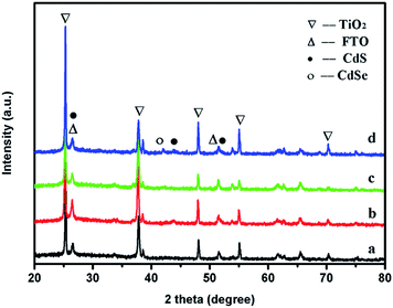 | ||
| Fig. 1 XRD patterns of (a) bare TiO2NSs, (b) TiO2NSs/CdS (30 min), (c) TiO2NSs/CdSe (10C) and (d) TiO2NSs/CdS (30 min)/CdSe (10C) samples. | ||
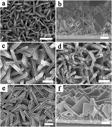
The vertically aligned {001} facets and the non-overlapping structures of the TiO2NSs are interlaced and interconnected. Fig. 1b shows the cross-section view of a TiO2NSs array film, which shows the vertical growth structure, and the thickness of the array film is about 3 μm. Fig. 2c and d show the top-section view of TiO2NSs/CdS (30 min) and TiO2NSs/CdSe (10C), respectively. Both samples retain their original morphology, but become relatively rough and possess uniform nanoparticles, indicating that CdS and CdSe QDs have been successfully deposited on the surface of the TiO2NSs array film. It is worth noting that the surface of the TiO2NSs array film was entirely covered with CdS QDs, but CdSe QDs were only adsorbed on a small section of the TiO2NSs surface, suggesting that the growth of CdSe on TiO2NSs is more difficult than that of CdS. Fig. 2e and f show the top view and cross-section view of TiO2NSs/CdS (30 min)/CdSe, respectively. A large number of CdS and CdSe QDs are deposited densely and uniformly on both the {001} and {101} facets of the TiO2NSs array film. In contrast to the CdSe single-sensitized samples, more CdSe QDs can be observed. This behaviour may be attributed to the fact that better lattice match between TiO2 and CdS assists the growth of CdSe, which is consistent with previous reports.32 Theoretical calculations have shown that the (110) plane of cubic CdS [(2 × 2) supercell parameters (11.65 × 8.24 Å2)] agrees best with the (101) plane of TiO2 [(2 × 2) supercell parameters (10.87 × 7.73 Å2)] with a lattice mismatch smaller than 7%. However, the mismatch between the (110) plane of cubic CdSe [(2 × 2) supercell parameters (12.11 × 8.56 Å2)] and the (101) plane of TiO2 is greater than 11%, suggesting that the growth of CdS on the TiO2 film is easier, and the growth of CdSe is difficult. This observation is also confirmed by the XRD results obtained in this study.
The composition and elemental distribution of the composite array films were investigated by elemental energy-dispersive spectroscopy (EDS) and EDS mapping. The EDS mapping images corresponding to the FESEM images in Fig. 2c–e are shown in Fig. S3–S5,† respectively. A typical EDS spectrum (Fig. S5g†) shows that the TiO2NSs/CdS (30 min)/CdSe (10C) sample is composed of Ti, O, Cd, S and Se elements. The EDS mapping images of Ti, O, Cd, S and Se elements are exhibited in Fig. S5b–f.† It can be seen that Ti, O, Cd, S and Se are homogenously distributed in the entire TiO2NSs/CdS (30 min)/CdSe (10C) sample, suggesting that the CdS and CdSe QDs are grown homogeneously onto the TiO2NSs array films. These results provide strong evidence for the successful coating of QDs on the surface of TiO2NSs array films.
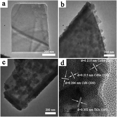 | ||
| Fig. 3 TEM images of (a) bare TiO2NSs, (b) TiO2NSs/CdS (30 min), and (c) TiO2NSs/CdS (30 min)/CdSe (10C). (d) HRTEM image of TiO2NSs/CdS (30 min)/CdSe (10C). | ||
Specifically, lattice fringes with interplanar spacing d (101) = 0.352 nm (Fig. 3d) is consistent with the anatase phase of TiO2 [JCPDS no. 21-1272]. The spacings of d (220) = 0.206 nm and d (220) = 0.215 nm correspond to the cubic phase of CdS [JCPDS no. 75-1546] and to the cubic phase CdSe [JCPDS no. 19-191], respectively.
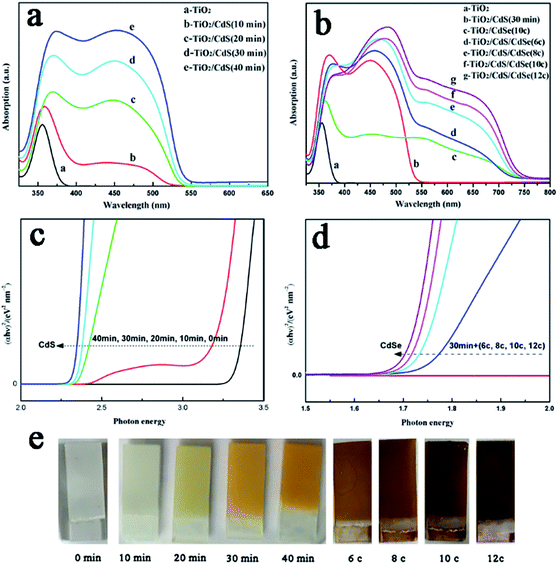
It should be noted that slight red shifts were observed with an increase in CdS deposition time or number of CdSe deposition cycles, corresponding to the growth of the QDs. As known from the quantum confinement effect, when the particle size decreases to the quantum scale, the number of atoms in a particle will significantly decrease, causing a larger gap between energy levels. Hence, the energy levels will change from a quasi-continuous phase to a split phase, and the energy gap will become wider, leading to the blue shift of the absorption. Therefore, it is thought that the growth of QDs is responsible for the slight red shift of the absorption edge.
The optical band gap Eg was calculated according to eqn (1), where α and ν are the absorption coefficient and the frequency, respectively.
| (αhν)2 = c(hν − Eg) | (1) |
The Eg values of photoelectrodes can be obtained by extrapolating the linear segment of the plots of (αhν)2-photon energy at α = 0. As illustrated in Fig. 4c and d, the calculated Eg of the TiO2NSs/CdS and TiO2NSs/CdS/CdSe films gradually decrease with an increase in CdS deposition time or number of CdSe deposition cycles.
3.2 Photovoltaic performance of the photoelectrodes
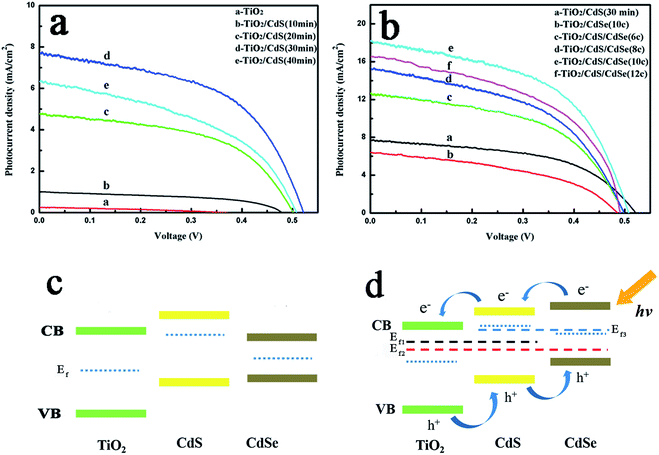
The photocurrent–voltage (J–V) curves of these devices are presented in Fig. 5 and the corresponding photovoltaic parameters are summarized in Table S1.†Fig. 5a shows the J–V curves of the TiO2NSs and TiO2NSs/CdS electrodes. The results indicate that the PCE of the devices is enhanced by increasing the CdS deposition time, which is due to the improved absorbance of visible light. However, when the deposition time reaches 40 min, the excessive amount of deposited CdS reduces the photovoltaic performance. This phenomenon may be attributed to the fact that excess deposited CdS would act as recombination centers for photo-generated carriers. The optimal deposition time found for the CdS-sensitized TiO2NSs photoelectrodes is about 30 min and the device exhibits an efficiency of 2.09%. The corresponding photovoltaic parameters are as follows: Voc = 0.52 V, Jsc = 7.68 mA cm−2, and FF = 0.52. We fabricated TiO2NSs/CdS/CdSe based on the TiO2NSs/CdS (30 min) photoelectrode and the corresponding J–V curves are shown in Fig. 4b. A similar phenomenon can be observed as previously discussed: the photocurrent density first increases and then decreases. When the number of SILAR cycles is 10C, the TiO2NSs/CdS/CdSe photoelectrode exhibits the highest efficiency of 4.77%, and the corresponding photovoltaic parameters are Voc = 0.51 V, Jsc = 18.22 mA cm−2, and FF = 0.52. It is worth noting that the TiO2NSs/CdSe (10C) sample shows much lower Jsc (6.42 mA cm−2) due to low coverage of CdSe on the TiO2NSs array film. All the TiO2NSs/CdS/CdSe photoelectrodes show higher efficiencies than the TiO2NSs/CdS electrode. Several factors are responsible for the enhanced photoelectric performance. First, the vertically aligned TiO2NSs array film retains both the advantage of sufficient surface area and photo-generated carrier transport path. Second, the significantly improved light absorption performance of the TiO2/CdS/CdSe photoelectrode due to the dense and uniform coverage of QDs on the TiO2NSs array film causes the increase in photocurrent density. Last, the energy level alignment at the TiO2NSs/CdS/CdSe interfaces produces a stepwise band edge structure, which can effectively separate and transfer the photo-generated carriers and induce higher resistance to the transport of excitons back to the electrolyte as shown in Fig. 5c and d. We also observed that Voc increased with CdS sensitization, but slightly decreased with the CdSe coating on TiO2NSs/CdS. The trend can be qualitatively evaluated from the shift in the Fermi level (Ef) because of the contact between CdS and CdSe. The variation of the Ef after CdS and CdSe sensitization is shown in Fig. 5c and d. Compared with bare TiO2NSs, the Ef shifts to more negative potentials upon sensitization with CdS for 30 min, which leads to an increase in Voc from 0.37 V to 0.52 V. When CdSe was deposited on the TiO2NSs/CdS (30 min) film, energy level realignment occurs in the TiO2NSs/CdS (30 min)/CdSe composite film photoelectrodes45 as shown Fig. 5d. However, the Ef of CdSe is less negative than that of CdS even after energy level realignment,12,46 which leads to the shift in the Ef of the TiO2NSs/CdS (30 min)/CdSe composite film to less negative values (from Ef1 to Ef2) and thus exhibits lower Voc than that of the TiO2NSs/CdS (30 min) composite film. In addition, the Voc of TiO2/CdSe with different layers is presented for better comparison. As shown in Fig. S6 and Table S1,† the Voc of TiO2/CdSe is lower than that of TiO2NSs/CdS (30 min)/CdSe. This is because Ef of CdSe is less negative than that of the realigned energy levels of CdS/CdSe (Ef3). Because the Ef of CdS and CdSe are both more negative than that of bare TiO2NSs, the Voc of TiO2NSs/CdS, TiO2NSs/CdSe, and TiO2NSs/CdS (30 min)/CdSe should also be larger than that of bare TiO2NSs.The monochromatic incident photon-to-electron conversion efficiency (IPCE) spectra (Fig. 6) clearly show that the photon-to-current responses of the TiO2NSs/CdSe (10C) and TiO2NSs/CdS (30 min)/CdSe (10C) devices exhibit significant red shifts compared with those of the TiO2NSs/CdS (30 min) device. The integrated Jsc for the corresponding devices, namely, TiO2NSs/CdS (30 min), TiO2NSs/CdSe (10C), and TiO2NSs/CdS (30 min)/CdSe (10C) are 7.34, 6.52 and 17.32 mA cm−2, respectively, which is consistent with the experimentally obtained Jsc. These results indicate that TiO2NSs/CdS (30 min)/CdSe (10C) photoelectrode not only has a broader light absorption range, but also has high IPCE value. These results also demonstrate that the stepwise band edge structure reduces charge recombination, resulting in more efficient photo-generated carrier separation and transfer. In addition, it is also demonstrated that the CdS QDs serve as a seed layer that promotes the growth of CdSe. The excellent IPCE value of the TiO2NSs/CdS/CdSe device manifested its great potential for the construction of high-performance QDSSCs.
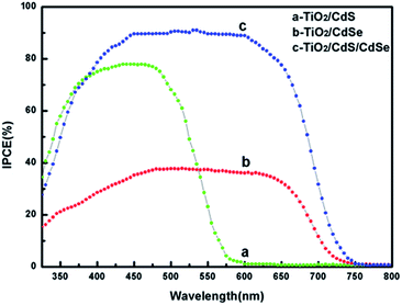 | ||
| Fig. 6 IPCE spectra of (a) TiO2NSs/CdS (30 min), (b) TiO2NSs/CdSe (10C), and (c) TiO2NSs/CdS (30 min)/CdSe (10C). | ||
Long-term stability is very important in the performance of solar cells. To prove the long-term stability of the photoelectrode, the photostability of TiO2NSs/CdS (30 min)/CdSe (10C) was measured for 1 h under continuous illumination. As shown in Fig. 7, a steady photocurrent is delivered by the device under 1 h-illumination with a drop in photocurrent of only 4% during this time. This result indicates that the TiO2NSs/CdS (30 min)/CdSe (10C) photoelectrode exhibits excellent long-term stability.
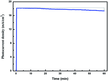 | ||
| Fig. 7 Photocurrent stability of TiO2NSs/CdS (30 min)/CdSe (10C) under continuous illumination of 100 mW cm−2. | ||
4. Conclusion
In summary, a vertically aligned TiO2NSs array film was applied in TiO2/CdS/CdSe solar cells for the first time. We demonstrated that the amount of CdS and CdSe QDs has a great effect on the photoelectric performance of the devices. When the CdS deposition time was 30 min and the number of CdSe deposition cycles was 10C, the highest efficiency of 4.77% was achieved under AM 1.5 G illumination with Voc = 0.51 V, Jsc = 18.22 mA cm−2, and FF = 0.52. The improved photoelectric performance is attributed to the excellent light absorption property and the effective separation and transfer of photo-generated charge. Moreover, the excellent IPCE value of the devices further confirmed the superiority of the composite photoelectrode based on vertically aligned TiO2NSs array films. The enhanced photoelectric performance demonstrates that the co-sensitized photoelectrode based on vertically grown TiO2NSs array films will play an essential role in the photovoltaic field.Conflicts of interest
There are no conflicts to declare.Acknowledgements
This study was financially supported by National Natural Science Foundation of China (No. 51272086). And the Technology Development Program of Jilin Province (Grant no. 20130206078GX).Notes and references
- M. Gratzel, Nature, 2001, 414, 338–344 CrossRef CAS PubMed.
- P. V. Kamat, J. Phys. Chem. Lett., 2013, 4, 908–918 CrossRef CAS PubMed.
- M. Ye, X. Gao, X. Hong, Q. Liu, C. He, X. Liu and C. Lin, Sustainable Energy Fuels, 2017, 1, 1217–1231 CAS.
- X. Wang, Z. Li, J. Shi and Y. Yu, Chem. Rev., 2014, 114, 9346–9384 CrossRef CAS PubMed.
- Z. Chen, D. Pan, Z. Li, Z. Jiao, M. Wu, C.-H. Shek, C. M. L. Wu and J. K. L. Lai, Chem. Rev., 2014, 114, 7442–7486 CrossRef CAS PubMed.
- D. Fattakhova-Rohlfing, A. Zaleska and T. Bein, Chem. Rev., 2014, 114, 9487–9558 CrossRef CAS PubMed.
- W. J. Ong, L. L. Tan, S. P. Chai, S. T. Yong and A. R. Mohamed, Nanoscale, 2014, 6, 1946–2008 RSC.
- Y. Zhao, H. Bala, W. Zhao, J. Chen, H. Li, W. Fu, G. Sun, J. Cao and Z. Zhang, Appl. Phys. Lett., 2014, 104, 013901 CrossRef.
- E. Guo, L. Yin and L. Zhang, CrystEngComm, 2014, 16, 3403–3413 RSC.
- Q. Wu, J. Hou, H. Zhao, Z. Liu, X. Yue, S. Peng and H. Cao, Dalton Trans., 2018, 47, 2214–2221 RSC.
- Y. Chen, Q. Tao, W. Fu, H. Yang, X. Zhou, S. Su, D. Ding, Y. Mu, X. Li and M. Li, Chem. Commun., 2014, 50, 9509–9512 RSC.
- S. Cheng, W. Fu, H. Yang, L. Zhang, J. Ma, H. Zhao, M. Sun and L. Yang, J. Phys. Chem. C, 2012, 116, 2615–2621 CAS.
- Y. Lai, Z. Lin, D. Zheng, L. Chi, R. Du and C. Lin, Electrochim. Acta, 2012, 79, 175–181 CrossRef CAS.
- Q. Chen, R. Tong, X. Chen, Y. Xue, Z. Xie, Q. Kuang and L. Zheng, Catal. Sci. Technol., 2018, 8, 1296–1303 CAS.
- H. G. Yang, C. H. Sun, S. Z. Qiao, J. Zou, G. Liu, S. C. Smith, H. M. Cheng and G. Q. Lu, Nature, 2008, 453, 638 CrossRef CAS PubMed.
- F. Li, J. Xu, L. Chen, B. Ni, X. Li, Z. Fu and Y. Lu, J. Mater. Chem. A., 2013, 1, 225 CAS.
- D. Wu, S. Zhang, S. Jiang, J. He and K. Jiang, J. Alloys Compd., 2015, 624, 94–99 CrossRef CAS.
- L. Jiang, L. Sun, D. Yang, J. Zhang, Y.-J. Li, K. Zou and W.-Q. Deng, ACS Appl. Mater. Interfaces, 2017, 9, 9576–9583 CAS.
- H. Zhou, L. Li, D. Jiang, Y. Lu and K. Pan, RSC Adv., 2016, 6, 67968–67975 RSC.
- J. Yu, J. Fan and K. Lv, Nanoscale, 2010, 2, 2144–2149 RSC.
- S. Hoang, S. P. Berglund, R. R. Fullon, R. L. Minter and C. B. Mullins, J. Mater. Chem. A., 2013, 1, 4307 CAS.
- P. K. Santra and P. V. Kamat, J. Am. Chem. Soc, 2012, 134, 2508–2511 CrossRef CAS PubMed.
- Y. Ding, T. Zhang, C. Liu, Y. Yang, J. Pan, J. Yao, L. Hu and S. Dai, Sustainable Energy Fuels, 2017, 1, 520–528 CAS.
- M. V. Vinayak, M. Yoosuf, S. C. Pradhan, T. M. Lakshmykanth, S. Soman and K. R. Gopidas, Sustainable Energy Fuels, 2018, 2, 303–314 CAS.
- T. R. Rana, S. Kim, J. Kim, K. Kim and J. H. Yun, Sustainable Energy Fuels, 2017, 1, 1981–1990 CAS.
- S. Kumar, M. Nehra, A. Deep, D. Kedia, N. Dilbaghi and K.-H. Kim, Renewable Sustainable Energy Rev., 2017, 73, 821–839 CrossRef CAS.
- J. H. Bang and P. V. Kamat, Adv. Funct. Mater., 2010, 20, 1970–1976 CrossRef CAS.
- Y. Lin, Y. Lin, Y. Meng, Y. Tu and X. Zhang, Opt. Commun., 2015, 346, 64–68 CrossRef CAS.
- J. Li, J. P. McClure, R. Fu, R. Jiang and D. Chu, Appl. Surf. Sci., 2018, 429, 48–54 CrossRef CAS.
- Z. Lu, J. Xu, X. Xie, H. Wang, C. Wang, S.-Y. Kwok, T. Wong, H. L. Kwong, I. Bello, C.-S. Lee, S.-T. Lee and W. Zhang, J. Phys. Chem. C, 2012, 116, 2656–2661 CAS.
- J. Zhang, C. Sun, S. Bai, R. Luo, A. Chen, L. Sun and Y. Lin, Electrochim. Acta, 2013, 106, 121–126 CrossRef CAS.
- B. Zhang, J. Zheng, X. Li, Y. Fang, L.-W. Wang, Y. Lin and F. Pan, Chem. Commun., 2016, 52, 5706–5709 RSC.
- X.-Q. Gong, A. Selloni, M. Batzill and U. Diebold, Nat. Mater., 2006, 5, 665 CrossRef CAS PubMed.
- S. S. Mali, R. S. Devan, Y.-R. Ma, C. A. Betty, P. N. Bhosale, R. P. Panmand, B. B. Kale, S. R. Jadkar, P. S. Patil, J.-H. Kim and C. K. Hong, Electrochim. Acta, 2013, 90, 666–672 CrossRef CAS.
- M. P. Genovese, I. V. Lightcap and P. V. Kamat, ACS Nano, 2012, 6, 865–872 CrossRef CAS PubMed.
- P. K. Santra, A. F. Palmstrom, J. T. Tanskanen, N. Yang and S. F. Bent, J. Phys. Chem. C, 2015, 119, 2996–3005 CAS.
- C. She, A. Demortière, E. V. Shevchenko and M. Pelton, J. Phys. Chem. Lett., 2011, 2, 1469–1475 CrossRef CAS.
- J. M. Azpiroz, E. Ronca and F. De Angelis, J. Phys. Chem. Lett., 2015, 6, 1423–1429 CrossRef CAS PubMed.
- X. Jin, H. Li, S. Huang, X. Gu, H. Shen, D. Li, X. Zhang, Q. Zhang, F. Li and Q. Li, J. Colloid Interface Sci., 2018, 510, 376–383 CrossRef CAS PubMed.
- S. A. Pawar, D. S. Patil, H. R. Jung, J. Y. Park, S. S. Mali, C. K. Hong, J.-C. Shin, P. S. Patil and J.-H. Kim, Electrochim. Acta, 2016, 203, 74–83 CrossRef CAS.
- X. Ma, Y. Shen, G. Wu, Q. Wu, B. Pei, M. Cao and F. Gu, J. Alloys Compd., 2012, 538, 61–65 CrossRef CAS.
- Y. Zhu, R. Wang, W. Zhang, H. Ge and L. Li, Appl. Surf. Sci., 2014, 315, 149–153 CrossRef CAS.
- Z. Peng, Y. Liu, Y. Zhao, K. Chen, Y. Cheng and W. Chen, Electrochim. Acta, 2014, 135, 276–283 CrossRef CAS.
- H. Yao, W. Fu, H. Yang, J. Ma, M. Sun, Y. Chen, W. Zhang, D. Wu, P. Lv and M. Li, Electrochim. Acta, 2014, 125, 258–265 CrossRef CAS.
- C.-F. Chi, H.-W. Cho, H. Teng, C.-Y. Chuang, Y.-M. Chang, Y.-J. Hsu and Y.-L. Lee, Appl. Phys. Lett., 2011, 98, 012101 CrossRef.
- Y.-L. Lee, C.-F. Chi and S.-Y. Liau, Chem. Mater., 2010, 22, 922–927 CrossRef CAS.
Footnote |
| † Electronic supplementary information (ESI) available. See DOI: 10.1039/c8se00084k |
| This journal is © The Royal Society of Chemistry 2018 |

