
Optimised heterojunctions between [100]-oriented rutile TiO2 arrays and {001} faceted anatase nanodomains for enhanced photoelectrochemical activity†
Alfonso
Ballestas-Barrientos
 a,
Xiaobo
Li
a,
Samuel
Yick
ab,
Anthony F.
Masters
a and
Thomas
Maschmeyer
*a
a,
Xiaobo
Li
a,
Samuel
Yick
ab,
Anthony F.
Masters
a and
Thomas
Maschmeyer
*a
aLaboratory of Advanced Catalysis for Sustainability, School of Chemistry, The University of Sydney, Sydney 2006, Australia. E-mail: thomas.maschmeyer@sydney.edu.au
bCSIRO Manufacturing, P.O. Box 218, Lindfield, NSW 2070, Australia
First published on 20th April 2018
Abstract
We report in this work the hydrothermal synthesis of [100]-oriented rutile TiO2 rods on FTO substrates. The presence of [100]-oriented rutile TiO2 nanorod arrays was confirmed using HRTEM and EBSD. It was found that by adjusting the concentration of HF, the growth of [100] oriented rutile TiO2 nanorod arrays and their heterojunctions with {001} faceted anatase TiO2 crystals can be achieved in a one-step synthesis procedure. The photoelectrochemical activity of the resulting thin films was tested in dihydrogen phosphate buffer (pH 7) and showed a dramatically increased activity. The photoelectrochemical activity, characterised using electrochemical impedance spectroscopy (EIS), revealed that contrary to the behaviour of the analogue anatase TiO2 phase, the presence of surface fluorine (F−) has a beneficial effect in the photoelectron transport properties within the rutile TiO2 phase. The methodology developed in this work also showcases the reliability of using Raman microscopy and EBSD in the detailed characterisation of surface defects which provides a new insight for the creation of new and improved photoanodes with enhanced photoelectrochemical activity for photoelectrochemical driven reactions.
Introduction
Non-renewable fuels such as coal, natural gas and petroleum remain as the dominant energy sources supporting global energy consumption. As energy demand increases, further reliance on these sources is expected, with the consequent increase of CO2 emissions. It is then imperative to create more efficient, accessible and more importantly, sustainable, ways to harness energy.With a high specific enthalpy of combustion (−286 kJ mol−1) and benign combustion product (water), molecular hydrogen remains the ideal renewable fuel when generated through the direct photo-catalysed or indirect (electrolysis) splitting of water.1 Among various catalysts, titanium dioxide (TiO2) functions as an effective photo-electro catalyst for the splitting of water as well as for the treatment of polluted air and water.2
It is known that the performance of TiO2 is strongly influenced not only by the presence of either one or both of the main TiO2 polymorphs; namely anatase and rutile TiO2 phases, but also by their degree of crystallinity and overall surface area.3–5 In addition, doping TiO2 crystals with transition and non-metals has been shown to be an effective strategy in improving the photoactivity6–9 as well as a means of creating oxygen vacancies by the production of highly active Ti3+ centres.10–12 Similarly, the formation of grain boundaries in polycrystalline TiO2 materials can improve their activity by the generation, at these boundary areas, of electric fields able to decrease the recombination rate of charge carriers.13
Following the crystal-facet engineering breakthrough made by Yang et al. using fluoride,14 the strategy of crystal growth in the presence of capping agents to induce the formation of high-surface-energy facets has become relevant for tailoring the properties of TiO2 for a variety of applications.2,15–17 This new synthetic strategy consists of altering the equilibrium crystal growth direction by using additives, or capping agents, which are adsorbed preferentially on high energy facets, thereby reducing their surface energies during growth and ultimately generating crystals with highly energetic exposed facets.16–22 By using this methodology, the synthesis of faceted TiO2 crystals has been explored for anatase14,18,20,23 and, to a lesser extent, for rutile TiO2.24–28 While these materials can be used for photocatalytic applications, their photoelectrochemical characterisation is limited by the ex situ deposition methodologies on conductive substrates during the preparation of photoanodes. The main challenges are two-fold, creating intimate contact between the TiO2 and the substrate, and controlling the orientation of the faceted crystals in order to ensure the exposure of the desired facet. In this sense, the in situ preparation of TiO2 films on conductive substrates can solve both of these issues by the direct nucleation and growth of oriented TiO2 crystals on Transparent Conducting Films (TCFs) or Ti foil by hydrothermal and anodisation methods.2 In the case of the rutile TiO2 phase, the direct hydrothermal growth of [001], [111] and [101] oriented crystals has been performed previously, as established using HRTEM and Raman spectroscopy as characterisation tools.10,12,26,29–31 In 2016, a modification of the method proposed by Liu and Aydil29 to produce [001] oriented TiO2 nanorod arrays was developed to hydrothermally synthesise [101] oriented rutile TiO2 nanorod arrays on FTO glass.31 They used TEM and tip-enhanced Raman to confirm the presence of the anatase phase. This allowed them to propose a mechanism for the enhancement in the photocatalytic activity in the (101) rutile-anatase TiO2 heterojunction.31 In spite of all these findings, and to our surprise, no hydrothermal method for the synthesis of a [100] oriented rutile TiO2 film has been reported. The properties of this facet have only been studied using commercial single crystals TiO2 (rutile) wafers doped with niobium oxide and having the desired facet cut and alkali-polished.32–35
In view of this, we report the first hydrothermal synthesis of [100] oriented rutile TiO2 nanorods array on FTO glass by using HF as capping agent. The use of HF in the synthesis of anatase films has been previously reported,14,20,22,23,36 however and as per our understanding, this is the first time the concentration of HF is controlled in order to achieve the formation of pure rutile TiO2 films. Furthermore in this work it is revealed that by adjusting the amount of HF in the reaction media we achieve the one step synthesis of both [100] rutile TiO2 and faceted {001} anatase TiO2 crystals resulting in a higher photoelectrochemical activity. The photoelectrochemical study revealed the beneficial effect of fluorine in the surface of rutile TiO2 while the opposite is observed for its analogous phase anatase.
To get a deeper insight regarding the crystal orientation, Electron Backscatter Diffraction (EBSD) was used on different areas of the films and the results correlated to XRD and site specific HRTEM. Although EBSD has become a popular technique in the analysis of materials in different fields such as ceramics, alloys, semiconductors and geology, its application in the study of crystal orientation on photocatalytic materials has hardly been exploited.37–39 One of the limitations of EBSD is the use of high acceleration voltages, which makes it unsuitable for materials with low conductivity. In this study, the high crystallinity of the TiO2 films allowed us to use lower acceleration voltages in the determination of the phase composition of the samples and the orientation of the crystals across different areas of the films. The results obtained in this work suggest for the first time that this technique can be effectively applied in the characterisation of films with photoelectrocatalytic applications, with special attention to the study of oriented crystalline films.
Experimental section
In a typical synthesis, 15 mL of deionized water was mixed with 15 mL of concentrated hydrochloric acid (32% by weight, Merck). To this, an aliquot of hydrofluoric acid (48% by weight, Sigma-Aldrich) was added and the solution stirred under ambient conditions for 5 min followed by the addition of 0.5 mL of titanium(IV) butoxide (97% Sigma-Aldrich). After stirring for another 5 min, the reaction mixture was separated into 3 × 10 mL solutions and each one was transferred to a Teflon-lined stainless steel autoclave. Finally, a piece of FTO substrate (F:SnO2, Tec 15, 15 Ω sq−1, Dyesol Limited), ultrasonically cleaned in successive baths of deionized water, acetone, and 2-propanol for 60 min, was placed at an angle against the wall of the Teflon-liner with the conducting side facing down. The hydrothermal synthesis was performed in air at 150 °C for 12 h in an electric oven. After synthesis, the autoclave was cooled to room temperature under flowing air. The FTO substrate was removed, rinsed extensively with deionized water and allowed to dry in ambient air. The amount of HF in the reaction mixture was changed from 0 to either 15 μL (0.05% v/v of the H2O![[thin space (1/6-em)]](https://www.rsc.org/images/entities/char_2009.gif) :HCl mixture) or 60 μL (0.2% v/v of the H2O:HCl mixture), with the corresponding samples being designated T0, T5 and T20. Defluorination of the samples was carried out after synthesis by thermally heating the samples to 600 °C at a ramping rate of 5 °C min−1 and then holding the temperature at 600 °C for 90 min. Thermally treated samples are referred to as T0-F, T5-F and T20-F, respectively.
:HCl mixture) or 60 μL (0.2% v/v of the H2O:HCl mixture), with the corresponding samples being designated T0, T5 and T20. Defluorination of the samples was carried out after synthesis by thermally heating the samples to 600 °C at a ramping rate of 5 °C min−1 and then holding the temperature at 600 °C for 90 min. Thermally treated samples are referred to as T0-F, T5-F and T20-F, respectively.
The crystal structure of the as-prepared film was examined by X-ray diffraction (XRD, PANalytical X'Pert PRO MPD) using Cu Kα (λ = 1.5419 Å) as the irradiation source. Morphological and lattice structural information were examined with Field Emission Scanning Electron Microscopy (FESEM, Zeiss ULTRA plus). The EBSD system was an Oxford Instruments AZtec v3.0 integrated EBSD and EDS system, equipped with a Nordlys Nano EBSD detector and an X-Max20 silicon drift EDS detector. Transmission Electron Microscopy (TEM) was performed using a JEOL 2200 at an acceleration voltage of 120 kV. Raman spectroscopy was performed using a Renishaw InVia Reflex System spectrometer (Renishaw plc). The power of the laser was 50 mW and the selected excitation wavelength was 488 nm with an exposure time of 5 s. X-ray photoelectron spectroscopy (XPS) was carried out using a Specs SAGE 150 system with the Mg Kα excitation at 1253.6 eV and a resolution of 0.8 eV. Both survey and narrow scans of Ti 2p, O 1s, F 1s and C 1s were obtained and the binding energies were corrected to the position of the C 1s peak defined as 284.60 eV. All photoelectrochemical (PEC) measurements were carried out at a scan rate of 10 mV s−1 using an eDAQ Potentiostat 466 system in a standard three electrode configuration using platinum mesh, Ag/AgCl (3 M) (BASi instruments, MF-2052) and the as-prepared samples as the counter, reference and working electrode, respectively. A buffer solution of 0.1 M Na2HPO4/NaH2PO4 adjusted to pH 7 was used as the electrolyte. Impedance measurements were performed with a BioLogic SP300 potentiostat in a similar setup as described in the cyclic voltammetry section. The frequency range applied was from 200 kHz to 10 mHz. The sinusoidal potential perturbation was 50 mV and the impedance spectra were analysed using the software package EC-Lab® V11.12. The illumination of 1 sun was simulated by a xenon lamp (Solar Light Co., XPS 400) and the irradiance of 100 mW cm−2 was checked using a photometer (Solar Light Co., PMA2100) connected to a calibrated pyranometer (Solar Light Co., PMA 2144).
Results and discussion
TiO2 crystals were hydrothermally synthesized using titanium(IV) butoxide as a starting material in the presence of a fixed amount of a 1:1 HCl:H2O mixture and different amounts of HF, the mixture heated at 150 °C for 12 h. XRD patterns (Fig. 1) show that at low HF concentrations (added aliquots of HF from 0 to 5 μL), only rutile TiO2 (SG, P42/mnm; JCPDS no. 88-1175, a = b = 0.4517 nm and c = 0.2940 nm)29 TiO2 was obtained. The enhancement of the (002) diffraction peak in the sample T0 (no HF added during synthesis) is related to the highly oriented crystals growing in the [001] direction perpendicular to the substrate surface.29 The diffractogram obtained for the T5 sample on the other hand showed only one main reflection corresponding to the (100) plane while the synthesis performed with a higher concentration of HF during the hydrothermal synthesis (0.2% v/v of the H2O:HCl mixture, sample T20) resulted in mixtures of anatase and rutile TiO2 phases. A lower intensity ratio between R(200) and the peak belonging to the FTO substrate was ascribed to the co-existence of anatase TiO2 and to the formation of a thinner TiO2 film (as shown later in Fig. 2e and h).
 | ||
| Fig. 1 XRD patterns for FTO glass (a) onto which TiO2 films were grown: (b) T0, (c) T5 and (d) T20. Note the intense 002 reflection for the T0 sample, described in the text. | ||
 | ||
| Fig. 2 SEM images of TiO2 films: T0 (a–c), T5 (d–f) and T20 (g–i). The images (c), (f) and (i) are those from heat treated samples T0-F, T5-F and T20-F, respectively. Scale bars correspond to 1 μm. | ||
It has been previously reported that high Cl− concentrations and strongly acidic media make the formation of the rutile TiO2 phase predominant at the expense of the anatase phase. By contrast, the presence of F− ions has been reported to promote anatase formation over that of rutile TiO2.2,20,26,28 For the sample T20, Grazing Incidence X-ray Diffraction (GIXRD, Fig. S1†) data were additionally collected with a grazing incidence angle of 1.5° in order to suppress the intense signal from the substrate. After calcination of the samples, the XRD patterns remained the same as shown in Fig. S2,† indicating that no change in the structure was induced by heating at the conditions described. The relative intensity of the R (002) diffraction peak with respect to the FTO diffraction peaks in the sample T5 increased after thermal treatment, a circumstance that indicates an improvement in the crystallinity of the film. The better crystallinity of the samples was also reflected in their optical properties as shown in Fig. S3.† In general, the thermally treated samples had lower energy offsets when compared to their untreated counterparts. However, this was also the case for the samples made without F− in the reaction medium. Therefore, these results are in this case consistent with the presence of surface F− not having a large impact on the band gap of the TiO2. Similar results have also been reported in previous studies in F− doped TiO2 samples and attributed to the fact that the energy levels of F 2p states of fluorine are below those of the O 2p in F-doped TiO2.40–43 The higher energy offsets in samples T20 and T20-F were related to the presence of anatase which has a larger energy band gap (3.0 and 3.2 eV for rutile and anatase TiO2 respectively).
The samples' morphologies were examined using SEM (Scanning Electron Microscopy). Fig. 2 shows the SEM images of the TiO2 films grown on FTO glass. Fig. 2a and b shows the formation of nanorods, which eventually tend to aggregate to form arrays by sharing their lateral facets. Sample T5 (Fig. 2d and e) consisted of nanorod structures with the additional formation of defects, which then grew outwards terminating in a hemispherical cap. Further addition of HF during the synthesis induced the formation of anatase in the form of microsheets (Fig. 2g–i). These results correlate well with the XRD patterns described above. From Fig. 2 it was evident that the T20 and T20-F films were thinner than those of the rest of the samples. While thinner films could be beneficial as they provide shorter distances for injected electrons to reach the FTO substrate, the reduction in bulk volume compromises the amount of light that can be absorbed by the film. The thickness of the sample plays an important role as it implies different widths in the space charge regions (also called the depletion layer) as discussed later in this work. The SEM images (Fig. 2f and i) also show that after calcination, pore formation occurred on the crystals' surfaces due to the erosion of F− ions. To ensure that F− ions had been completely removed, the elemental composition on the surface of the films was studied by using XPS of the uncalcined and calcined films (Fig. 3 and S4†). The XPS spectra of the calcined samples did not show any significant F 1s peaks, the absence of which indicates the annealing treatment was effective for both T5 and T20 samples. Atomic composition analyses (Fig. 3b, c and S4b†) further confirm the absence of F− on the surfaces of the calcined samples.
 | ||
| Fig. 3 XPS spectra measured for T5 (a and b) and T5-F (c) samples. (a) shows the full-scan XPS spectrum and (b and c) show the narrow scan for the F 1s peak for the samples T5 and T5-F respectively. | ||
EBSD was applied for the first time not only in the phase characterisation of the films but also in the determination of the crystal growth direction of TiO2 rods array. Fig. 4 show the band contrast (Fig. 4a), phase map (Fig. 4b) and orientation map (Fig. 4c–e) for the sample T0 made according to the original method proposed by Liu and Aydil.29 The band contrast and phase map indicate the presence of well-defined grains corresponding to the rutile TiO2 phase. The orientation map, showed as an inverse pole figure (IPF Z) was taken choosing the surface-normal direction as the reference sample direction and the Z axes of the crystal as viewing direction. The predominant red colour shown on the orientation map (Fig. 4c) clearly indicates the preferential orientation of the rods in one direction, which corresponds to the [001] crystal direction parallel to the sample normal as explained in the IPF legend (Fig. 4d). The contoured inverse pole figure (Fig. 4e) corroborates that all the grains were oriented in the [001] crystal direction parallel to the sample normal, this prevalent orientation is characteristic of a film with a strong texture. It is noteworthy that these results correlate well with the results shown in the XRD analysis so this technique could be used to characterised photoanodes' texture and phase composition.
 | ||
| Fig. 4 EBSD mapping obtained for sample T0 showing (a) pattern quality map, (b) phase mapping (red colour indicates the points where rutile was indexed from the transmission Kikuchi diffraction patterns, TKDPs) and (c) orientation map showing the Inverse Pole Figures (IPF) with respect to Z axis, perpendicular to the sample substrate (IPF ‖ Z), (d) IPF colour key used in the construction of the orientation map in (c). (e) shows the contoured inverse pole figures with respect to the X, Y and Z axes separately. | ||
Fig. 5 on the other hand, shows the results obtained for the sample T5. The pattern quality map (Fig. 5a) indicates well-defined grains produced by the lateral aggregation of individual TiO2 rods as well as grains with different sizes and shapes. The areas adjacent to the larger grains could not be resolved due to poor diffraction patterns caused by shadow effects of these large particles. The phase map (Fig. 5b) confirmed the predominant presence of TiO2 in the rutile phase throughout the entire film.
 | ||
| Fig. 5 EBSD mapping obtained for sample T5 showing (a) pattern quality map, (b) phase mapping (red colour indicates the points where rutile was indexed from the transmission Kikuchi diffraction patterns, TKDPs) and (c) orientation map showing the Inverse Pole Figures (IPF) with respect to Z axis, perpendicular to the sample substrate (see IPF colour key on Fig. 4d), (d) contoured IPF (with respect to X, Y and Z, separately). | ||
The orientation map shown as an inverse figure (Fig. 5c) clearly shows the prevalent orientation of the crystals with the [100] direction growth perpendicular to the sample substrate. Fig. 5c also revealed that the large grains grew with a different crystal orientation as it could be predicted from the Fig. 2d. The presence of grains with different orientation makes possible the formation of high-angle grain boundaries (disorientation angles higher than 15°) with a respective increase of the photoelectrochemical activity. With respect to this, Masayuki has artificially prepared bicrystalline TiO2 samples and studied the effect of grain boundaries on the photocatalytic activity of the samples.13 Masayuki's work revealed an enhanced charge separation on the samples where crystals' boundaries imperfections existed. These dislocations of the crystals induce the bending of the band structure,13 thereby suppressing the recombination of charge carriers and enhancing the photocatalytic activity of the samples. In the present work, the addition of HF during the synthesis induced the growth of a [100] oriented rutile TiO2 nanorods array with a high density of crystal boundaries by stabilizing the growth of grains in different crystals' direction.
HRTEM and SAED (Selected Area Electron Diffraction) were used in combination to test the EBSD results and get more information about the presence of grain boundaries. To do this a SEM-FIB system with a micromanipulator was used in order to extract a region of the film where big grain formation took place. The electron diffraction patterns could be indexed to the rutile TiO2 phase as shown in the insets of Fig. 6b and c. From both insets in Fig. 6 it is clear that both grains grew in the [100] crystal direction, however, the orientations of the two crystals were different. Overlapping of the two data sets (Fig. 6d) allowed the determination of the orientation relationship between the two grains, i.e. the crystal direction g1[100] is rotated by 57° with respect to the g2[100]. This translates in the formation of intergrown crystals with arbitrary orientations. These particles were distributed randomly on the surface and, as seen in Fig. 2d, they were formed at some point during the growth of the TiO2 rods.
 | ||
| Fig. 6 HRTEM study of T5: (a) SEM image showing a defect area and its HRTEM image (b) and a non-defect area with its HRTEM image (c); insets in (b) and (c) correspond to their respective SAED patterns and their combination is shown in (d). | ||
Raman spectroscopy (in the form of Raman microscopy) was used to reveal the distribution of surface energies along the surface of the [100] oriented rutile TiO2 nanorods array. This is achieved by mapping of the Raman spectra of TiO2 on various regions of the films. Fig. S5† shows a typical Raman spectrum measured for the T5 sample. As shown in this figure, four Raman vibrational modes were observed. These are attributed to the rutile TiO2 phase (tetragonal space group P42/mnm) and they corresponded to the Eg, multi-proton, A1g and B2g vibrational modes.44 It has been shown that the intensity ratios of different vibrational modes in the Raman spectrum can be related different facets energies.23,44 In the present study, the intensity ratios between the A1g and Eg vibrational modes of the rutile TiO2 phase were determined for all the spectra taken during the mapping study. In this interpretation, facets with lower surface energy will mostly present saturated 6c-Ti and 3c-O bonding modes, while surfaces with higher energy consist of unsaturated 5c-Ti and 2c-O bonding modes.44 As the symmetric stretching vibration (Eg) is enhanced by saturated modes, and considering that unsaturated 5c-Ti and 2c-O bonding modes exhibit higher B1g and A1g intensities, then a higher A1g/Eg intensity ratio indicates a higher surface energy related to different exposed facets.23
Fig. 7 shows the map of the A1g/Eg Raman intensity ratio for the T5 sample. The map taken for sample T5 indicates that facets with higher surface energy were formed where defect formation took place. These results show that HF can be used as a capping agent in the hydrothermal synthesis of TiO2 films used as photoanodes. The Raman mapping in Fig. 7 clearly indicates the stabilisation effect of HF in the formation of faceted crystals during the deposition on the FTO glass. This results in high surface energy facets being exposed due to the presence of coordinatively unsaturated Ti and O atoms.
 | ||
| Fig. 7 White light image (left) and map of the A1g/Eg Raman intensity ratio (right) for rutile T5 samples (the A1g/Eg Raman intensity ratio is depicted by colour changes as outlined in the legend). | ||
The EBSD data obtained for the T20 sample are shown in Fig. 8; from these data it is evident that the formation of both rutile and anatase TiO2 phases occurred in the T20 sample, the latter phase corresponding to the microsheets shown on the above mentioned figure as indicated by the phase map (Fig. 8c). Moreover, Fig. 8d–f revealed the simultaneous formation of rutile TiO2 [100] oriented crystals and {001} faceted anatase microsheets as shown by the contoured IPF (Fig. 8e–g). It has been shown that the synthesis of {001} faceted anatase microsheets can be achieved by using F− as a capping agent14,36,45 however in this work we are able to synthesise a facet specific rutile-anatase heterojunction in one single step with the preferential grow of {001} faceted anatase crystals. The photocurrents, as predictors of photoelectrochemical activity of the samples, were tested in neutral pH using a phosphate buffer as electrolyte.
 | ||
| Fig. 8 (a) SEM image of sample T20 indicating the area analysed by EBSD mapping, (b) pattern quality map of the magnified section of (a), (c) phase mapping (red and blue colours indicate the points where rutile and anatase were indexed respectively from the transmission Kikuchi diffraction patterns, TKDPs) and (d) orientation map showing the Inverse Pole Figures (IPF) with respect to Z axis, perpendicular to the sample substrate (see IPF colour key on Fig. 4d), (e and f) contoured IPF with respect to the Z axis for the rutile and anatase phase respectively. Figure (g) depicts the facet composition of the anatase TiO2 microsheets (shown in phase map, (c)). | ||
Fig. 9 shows the comparison between the photocurrent voltage curves of samples with and without thermal treatment. At this point it is important to mention that the use of other concentrations of HF during the synthesis of the TiO2 films resulted in lower photoelectrochemical activity. By adjusting the concentration of HF, the amount of anatase could be modified resulting in a lower photocurrent even for the calcined samples as shown Fig. S6 and S7.† These results indicate that by using 0.2% v/v of HF, the rutile to anatase TiO2 ratio was optimized, resulting in the highest photocurrent. In the absence of thermal defluorination, the T5 sample made of [100] oriented rutile TiO2 nanorods had the highest photocurrent efficiency. However, the T20 sample containing both anatase and rutile TiO2 phases prepared by further addition of HF (T20) during the hydrothermal synthesis exhibited a significant decrease in the photocurrent efficiency relative to the T5 sample. The samples with the lowest photocurrents/voltage were (i) those synthesised without using any F− capping agent (Fig. 9a) and (ii) the samples consisting mainly of anatase microsheets that were prepared using concentrations of HF higher than 0.2% v/v. It can be seen from these results that the phase obtained as well as the presence of F− on the surface play a significant role in the profiles of the photocurrent/voltage curves and hence likely photoelectrochemical activity of the TiO2 films.
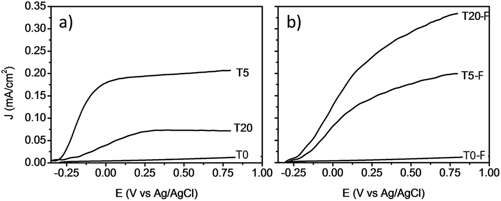 | ||
| Fig. 9 J–V plots of voltammograms at a light intensity of 100 mW cm−2 for TiO2 photoanodes without (left) and with (right) calcination. | ||
The removal of F− ions as a result of the calcination resulted in a higher photocurrent for the T20-F sample as can be seen from Fig. 9b. Previous literature suggests that the presence of F− ions on the surface of {001} faceted TiO2 nanosheets is detrimental to the photocatalytic activity of these materials.14,46–48 Thus, the present enhancement of the photocurrent efficiency could be related then to the detachment of surface F− ions. A recent study by Zhao and co-workers indicated that by annealing a layer of amorphous TiO2 deposited on FTO glass, the efficient growth of vertically aligned anatase TiO2 microsheets can be induced. The calcination of such a bilayer system resulted in an improved photoelectrochemical activity; however, no study has been reported regarding the effect of the presence of F− ions on the photocatalytic activity of these anatase TiO2 crystals with high energy surface facets.2,14,20,21,47 It is evident that the presence of F− on the surface of TiO2 based films has a different impact depending on the phase and the facet onto which it is bonded, resulting in different photoelectrochemical activity as shown on Fig. 9a and b. It is also likely that a higher surface area would result from the porosity induced by the escape of surface F− during the thermal treatment, as observed by Zou et al.21
A noteworthy aspect to consider regarding Fig. 9 is the shift of the onset potential for the thermally treated samples. This could be attributed to changes in the position of the conduction band of the films.12,49 The onset potentials were cathodically shifted for the T5 and T20-F samples compared to the T5-F and T20 samples respectively. This lower onset potential for the T5 and T20-F samples is consistent with the beneficial effect of F− on [100] oriented rutile TiO2, while the opposite is observed for the anatase TiO2 (resulting in a higher onset potential for the T20 sample). Another feature observed in Fig. 9 is the difference in the slopes for all the samples with and without thermal treatment. As the gradient of the photocurrent density vs. potential increases, the resistance for the charge transfer at the electrode/electrolyte interface is lower resulting in a better performance. To get further insight about the electron transport properties of the films at the electrode/electrolyte interface, electrochemical impedance spectroscopy (EIS) analysis was carried out in phosphate buffer and the typical Nyquist plots are shown in Fig. 10. It is evident that the arc radius for the T0 sample was considerably larger than those for the rest of the samples, T5 having by far the smallest radius. It is reported that the size of the arc radius in the Nyquist plot is related to the charge-transfer resistance at the electrode/electrolyte interface. In this sense, a smaller radius in the Nyquist plot is related to a lower resistance and better charge separation of electron–hole pairs.50,51 The impedance data set shown in Fig. 10 were fitted to an equivalent circuit model (Fig. 10c) using the Zfit package included in the EC-Lab V11.12® software with the results given in Table S1.† In this work, constant phase elements (CPEs) were used instead of capacitive elements to get the best fit (see fitting procedure details in footnote of Table S1†). In the circuit model shown in Fig. 10c, the resistance R1 simulates the solution resistance as well as other uncompensated resistances. Q1 simulates the capacity of the double electric layer and the charge transfer resistance. The R2 value represents the charge transfer resistance, which is the key parameter for this work. Interestingly, for the samples made using HF as capping agent, Q2 and R3 were necessary to be added to get the best fit, indicating the capacitance and resistance of the adsorbed layer of species (likely F−).52 As anticipated from the Nyquist plot of Fig. 10a, the charge transfer resistance on the surface of the photoanodes decreased drastically from the T0 to the T5 sample. The resistance estimated for the other samples showed similar values, but they were considerably below the R2 value obtained for the T0 sample. These results confirm that the presence of surface F− has a beneficial impact in the charge transfer properties of [100] oriented rutile TiO2 in comparison with its analogous anatase phase. Moreover, the a1 values were considerably smaller for the samples made using HF as capping agent, being the lowest for the T20 and T20-F samples. This effect has been observed on very thin samples, where the space charge layer is much smaller and the surface roughness becomes important in the capacity behaviour.52,53
 | ||
| Fig. 10 (a) Measured Nyquist plots for TiO2 base photoanodes with and without thermal calcination. Inset (b) indicates the magnified Nyquist plot of T5 sample and (c) shows the circuit model used to estimate the charge transfer resistance (R2) for the TiO2 samples. Measurement conditions as described in the Experimental section. | ||
The observation of Fig. 10 reveals that the film made with the [001] oriented rutile TiO2 nanorods array showed the highest charge transfer resistance while the T5 sample showed the lowest resistance. Moreover, thermal treatment of the T5 sample resulted in a higher resistance with respect to the untreated T5 sample indicating that surface F− ions are favourable for the photoelectrochemical activity of the [100] oriented rutile TiO2 array. While the Nyquist plot for the T20 sample indicates a higher resistance compared to the T5 sample, the results obtained for the T20-F seem not to be in accord with the higher photocurrent efficiency observed on the J–V plot shown on Fig. 9b. It is likely that the thinner depletion layer has a beneficial effect in the photoelectrochemical activity of the T20-F sample.
The photoelectrochemical study indicates that the charge transfer resistance at the electrode/electrolyte interface is dramatically lower for the [100]-oriented rutile TiO2 nanorod array reported in this work. However, Fig. 10 demonstrates that the resistance at the photoanode interface is not the mechanism for the enhancement of the activity found on the T20-F film. It is commonly found in the literature that the TiO2 anatase phase is more photoactive than is the rutile TiO2 phase. This fact is attributed to, among other parameters, differences in the electronic properties such as higher mobility of charge carriers for the anatase phase as well as a higher surface area and longer lifetimes of the electron–hole pairs.54,55 Interestingly, the growth of anatase microsheets on FTO using 1% v/v of HF resulted in a lower photocurrent with respect to the T20 sample (Fig. S6a†). The same effect was observed for the samples with thermal treatment (Fig. S6b†). It is relevant to mention that the heterojunction between the rutile and anatase phases has proven to have a synergetic effect on the photocatalytic activity of TiO2 based photocatalysts. This enhancement effect has also been observed between other TiO2 phases such as anatase and TiO2(B)56–58 and even between different materials59–61 as described by Zhu et al. Thus, the presence of both phases allows for a better electron–hole separation due to the higher energy of the conduction band for the anatase phase.62–65 Moreover, as the position of the conduction band in well-faceted crystals depends on the total surface energy,18,31,66 the formation of {001} faceted anatase crystals with high surface energy results in a higher energy conduction band for this phase.
Additionally, compared to the (001), (011) rutile TiO2 facets, the (100) facet has a much lower surface energy (28.9, 24.4 and 19.6 meV au−2, respectively),2 which lowers the energy of the conduction band in the rutile TiO2 phase. In this sense, the synthesis of rutile TiO2 films with exposed (100) facets in heterojunctions with {001} faceted anatase TiO2 crystals translates into a larger difference between the conduction band energies of the two phases and an improved charge separation at the interface of the two phases as depicted in Fig. 11. In this work, the synthesis of films consisting of an array of [100] oriented nanorods in conjunction with high energy {001} faceted anatase crystals is conveniently performed in a one-step synthesis resulting in a high photoelectrochemical activity after thermal removal of F− ions from the surface.
 | ||
| Fig. 11 Energy diagram of {001} faceted anatase microsheets in heterojunction with different rutile TiO2 facets (001 facets and the 100 facets made in this work). | ||
Finally, the photocurrent efficiency (η) calculated for the sample T20-F was estimated considering the pH used (pH 7) by the expression E(RHE) = EAg/AgCl + 0.059 pH + EoAg/AgCl (0.1976 V). The η value at 0.73 VRHE was 0.08%, which is lower than that reported for pristine TiO2 at the same voltage (0.37%)67 in NaOH 1 M as electrolyte. It is noteworthy that a comparison of the efficiency using NaOH as electrolyte for the samples made in this work was not possible since under this condition (high pH) defluorination of the photoanodes is induced. Further work is currently being performed by the authors to increase the photoelectrochemical efficiency of these films and to optimise the heterojunction between preferentially oriented rutile TiO2 and the anatase phase.
Conclusions
This work showcases the application of crystal and facet engineering combined with a set of characterization techniques (EBSD, site-specific HRTEM and Raman microscopy) to provide otherwise unobtainable insights in the development of materials for photoelectrochemical driven water splitting. The successful application of HF in the hydrothermal growth of TiO2 photoanodes on FTO glass to enhance the photoelectrochemical activity is described. The hydrothermal synthesis of [100] oriented rutile TiO2 nanorods was achieved for the first time by adjusting the concentration of HF to 0.05% v/v of HF during the reaction. Moreover, by increasing the concentration of HF to 0.2% v/v the intergrowth of these crystals and {001} faceted anatase TiO2 microsheets was accomplished in this work. This protocol gives the films with the best performance in phosphate buffer in water splitting which is expected for photoanodes presenting this kind of synergetic heterojunction. The study of the charge transfer resistance at the electrode/electrolyte interface using EIS, revealed that the presence of F− ions at the surface plays a key role in the charge transfer at the interface being unexpectedly beneficial in the case of [100] oriented rutile TiO2. Finally, to our knowledge this is the first time the hydrothermal synthesis of [100] oriented rutile TiO2 nanorods array is carried out and the co-growth of {001} faceted TiO2 anatase microsheets can be achieved in one step synthesis.Conflicts of interest
There are no conflicts to declare.Acknowledgements
The authors acknowledge the facilities and the scientific and technical assistance of the Australian Microscopy & Microanalysis Research Facility at the Australian Centre for Microscopy & Microanalysis at the University of Sydney. We also thank the Vibrational Spectroscopy Core Facility (VSCF) of the University of Sydney and the Commonwealth Scientific and Industrial Research Organisation (CSIRO). A. R. B.-B. also thanks the Australian Government Department of Education and Training for an Endeavour International Postgraduate Research Scholarship under the Grantee ID 4448_2015.References
- A. Fujishima and K. Honda, Nature, 1972, 238, 37–38 CrossRef CAS PubMed
.
- G. Liu, H. G. Yang, J. Pan, Y. Q. Yang, G. Q. Lu and H.-M. Cheng, Chem. Rev., 2014, 114, 9559–9612 CrossRef CAS PubMed
- X. Chen, Z. Zhang, L. Chi, A. K. Nair, W. Shangguan and Z. Jiang, Nano-Micro Lett., 2016, 8, 1–12 CrossRef CAS
- M. Gao, L. Zhu, W. L. Ong, J. Wang and G. W. Ho, Catal. Sci. Technol., 2015, 5, 4703–4726 CAS
- M. Matsuoka, M. Kitano, M. Takeuchi, K. Tsujimaru, M. Anpo and J. M. Thomas, Catal. Today, 2007, 122, 51–61 CrossRef CAS
- Z. Adriana, Recent Pat. Eng., 2008, 2, 157–164 CrossRef
- M. Pelaez, N. T. Nolan, S. C. Pillai, M. K. Seery, P. Falaras, A. G. Kontos, P. S. M. Dunlop, J. W. J. Hamilton, J. A. Byrne, K. O'Shea, M. H. Entezari and D. D. Dionysiou, Appl. Catal., B, 2012, 125, 331–349 CrossRef CAS
- B. Roose, S. Pathak and U. Steiner, Chem. Soc. Rev., 2015, 44, 8326–8349 RSC
- N. u. Saqib, R. Adnan and I. Shah, Environ. Sci. Pollut. Res., 2016, 23, 15941–15951 CrossRef CAS PubMed
- X. Liu, H. Zhang, X. Yao, T. An, P. Liu, Y. Wang, F. Peng, A. R. Carroll and H. Zhao, Nano Res., 2012, 5, 762–769 CrossRef CAS
- J.-Y. Ruzicka, F. A. Bakar, L. Thomsen, B. C. Cowie, C. McNicoll, T. Kemmitt, H. E. A. Brand, B. Ingham, G. G. Andersson and V. B. Golovko, RSC Adv., 2014, 4, 20649–20658 RSC
- H. Zhang, X. Liu, Y. Wang, P. Liu, W. Cai, G. Zhu, H. Yang and H. Zhao, J. Mater. Chem. A, 2013, 1, 2646–2652 CAS
- K. Masayuki, Appl. Phys. Express, 2008, 1, 101201 CrossRef
- H. G. Yang, C. H. Sun, S. Z. Qiao, J. Zou, G. Liu, S. C. Smith, H. M. Cheng and G. Q. Lu, Nature, 2008, 453, 638–641 CrossRef CAS PubMed
- W. Q. Fang, X. L. Wang, H. Zhang, Y. Jia, Z. Huo, Z. Li, H. Zhao, H. G. Yang and X. Yao, J. Mater. Chem. A, 2014, 2, 3513–3520 CAS
- C. Li, C. Koenigsmann, W. Ding, B. Rudshteyn, K. R. Yang, K. P. Regan, S. J. Konezny, V. S. Batista, G. W. Brudvig, C. A. Schmuttenmaer and J.-H. Kim, J. Am. Chem. Soc., 2015, 137, 1520–1529 CrossRef CAS PubMed
- S. K. Wallace and K. P. McKenna, J. Phys. Chem. C, 2015, 119, 1913–1920 CAS
- J. Pan, G. Liu, G. Q. Lu and H.-M. Cheng, Angew. Chem., Int. Ed., 2011, 50, 2133–2137 CrossRef CAS PubMed
- S. Yang, B. X. Yang, L. Wu, Y. H. Li, P. Liu, H. Zhao, Y. Y. Yu, X. Q. Gong and H. G. Yang, Nat. Commun., 2014, 5, 5355–5361 CrossRef CAS PubMed
- H. Zhang, Y. Wang, P. Liu, Y. Han, X. Yao, J. Zou, H. Cheng and H. Zhao, ACS Appl. Mater. Interfaces, 2011, 3, 2472–2478 CAS
- L. Pan, J.-J. Zou, S. Wang, X.-Y. Liu, X. Zhang and L. Wang, ACS Appl. Mater. Interfaces, 2012, 4, 1650–1655 CAS
- H. Wang, M. Liu, C. Yan and J. Bell, Beilstein J. Nanotechnol., 2012, 3, 378–387 CrossRef PubMed
- F. Tian, Y. Zhang, J. Zhang and C. Pan, J. Phys. Chem. C, 2012, 116, 7515–7519 CAS
- E. Bae, N. Murakami and T. Ohno, J. Mol. Catal. A: Chem., 2009, 300, 72–79 CrossRef CAS
- J. S. Chen and X. W. Lou, Chem. Sci., 2011, 2, 2219–2223 RSC
- K. Kakiuchi, E. Hosono, H. Imai, T. Kimura and S. Fujihara, J. Cryst. Growth, 2006, 293, 541–545 CrossRef CAS
- Z. Lai, F. Peng, H. Wang, H. Yu, S. Zhang and H. Zhao, J. Mater. Chem. A, 2013, 1, 4182–4185 CAS
- H. Wu, H. Li, J. Li, B. Lu, Y. Yang, W. Yuan, Y. Wang and Z. Zhang, CrystEngComm, 2015, 17, 7254–7257 RSC
- B. Liu and E. S. Aydil, J. Am. Chem. Soc., 2009, 131, 3985–3990 CrossRef CAS PubMed
- T. Sun, Y. Wang, M. Al-Mamun, H. Zhang, P. Liu and H. Zhao, J. Phys. Chem. C, 2015, 119, 17680–17686 CAS
- H. Sutiono, A. M. Tripathi, H.-M. Chen, C.-H. Chen, W.-N. Su, L.-Y. Chen, H. Dai and B.-J. Hwang, ACS Sustainable Chem. Eng., 2016, 4, 5963–5971 CrossRef CAS
- A. Y. Ahmed, T. Oekermann, P. Lindner and D. Bahnemann, Phys. Chem. Chem. Phys., 2012, 14, 2774–2783 RSC
- A. Imanishi, T. Okamura, N. Ohashi, R. Nakamura and Y. Nakato, J. Am. Chem. Soc., 2007, 129, 11569–11578 CrossRef CAS PubMed
- A. Imanishi, H. Suzuki, N. Ohashi, H. Kondoh, T. Ohta and Y. Nakato, J. Phys. Chem. C, 2009, 113, 17254–17261 CAS
- R. Nakamura, N. Ohashi, A. Imanishi, T. Osawa, Y. Matsumoto, H. Koinuma and Y. Nakato, J. Phys. Chem. B, 2005, 109, 1648–1651 CrossRef CAS PubMed
- B. Liu and E. S. Aydil, Chem. Commun., 2011, 47, 9507–9509 RSC
- M. Nishikawa, S. Yuto, T. Nakajima, T. Tsuchiya and N. Saito, Catal. Lett., 2017, 147, 292–300 CrossRef CAS
- D. Mateo, I. Esteve-Adell, J. Albero, J. F. S. Royo, A. Primo and H. Garcia, Nat. Commun., 2016, 7, 11819 CrossRef PubMed
-
Z. Chen, Y. Yang and H. Jiao, in Scanning Electron Microscopy, ed. V. Kazmiruk, InTech, Rijeka, 2012, ch. 4, DOI:10.5772/35267
- K. Yang, Y. Dai, B. Huang and M.-H. Whangbo, Chem. Mater., 2008, 20, 6528–6534 CrossRef CAS
- D. Li, H. Haneda, S. Hishita, N. Ohashi and N. K. Labhsetwar, J. Fluorine Chem., 2005, 126, 69–77 CrossRef CAS
- E. M. Samsudin and S. B. Abd Hamid, Appl. Surf. Sci., 2017, 391, 326–336 CrossRef CAS
- D. Li, H. Haneda, S. Hishita and N. Ohashi, Chem. Mater., 2005, 17, 2596–2602 CrossRef CAS
- J. Yan, G. Wu, N. Guan, L. Li, Z. Li and X. Cao, Phys. Chem. Chem. Phys., 2013, 15, 10978–10988 RSC
- Q. Li, T. Li, S. Chang, Q. Tao, B. Tian and J. Zhang, CrystEngComm, 2016, 18, 5074–5078 RSC
- X. Han, Q. Kuang, M. Jin, Z. Xie and L. Zheng, J. Am. Chem. Soc., 2009, 131, 3152–3153 CrossRef CAS PubMed
- Y. Lu, G. Wang, H. Zhang, Y. Zhang, S. Kang and H. Zhao, RSC Adv., 2015, 5, 55438–55444 RSC
- H. G. Yang, G. Liu, S. Z. Qiao, C. H. Sun, Y. G. Jin, S. C. Smith, J. Zou, H. M. Cheng and G. Q. Lu, J. Am. Chem. Soc., 2009, 131, 4078–4083 CrossRef CAS PubMed
- R. Beranek, Adv. Phys. Chem., 2011, 2011, 20 Search PubMed
- Z. Jiang, Y. Tang, Q. Tay, Y. Zhang, O. I. Malyi, D. Wang, J. Deng, Y. Lai, H. Zhou, X. Chen, Z. Dong and Z. Chen, Adv. Energy Mater., 2013, 3, 1368–1380 CrossRef CAS
- S. Zhu, T. Xu, H. Fu, J. Zhao and Y. Zhu, Environ. Sci. Technol., 2007, 41, 6234–6239 CrossRef CAS PubMed
-
H. Cesiulis, N. Tsyntsaru, A. Ramanavicius and G. Ragoisha, in Nanostructures and Thin Films for Multifunctional Applications: Technology, Properties and Devices, ed. I. Tiginyanu, P. Topala and V. Ursaki, Springer International Publishing, Cham, 2016, pp. 3–42, DOI:10.1007/978-3-319-30198-3_1
-
J. C. Alexander, in Surface Modifications and Growth of Titanium Dioxide for Photo-Electrochemical Water Splitting, Springer International Publishing, Cham, 2016, pp. 179–220, DOI:10.1007/978-3-319-34229-0_6
- D. A. H. Hanaor and C. C. Sorrell, J. Mater. Sci., 2011, 46, 855–874 CrossRef CAS
- Y. Kakuma, A. Y. Nosaka and Y. Nosaka, Phys. Chem. Chem. Phys., 2015, 17, 18691–18698 RSC
- D. Yang, H. Liu, Z. Zheng, Y. Yuan, J.-c. Zhao, E. R. Waclawik, X. Ke and H. Zhu, J. Am. Chem. Soc., 2009, 131, 17885–17893 CrossRef CAS PubMed
- H. Liu, Z. Zheng, D. Yang, X. Ke, E. Jaatinen, J.-C. Zhao and H. Y. Zhu, ACS Nano, 2010, 4, 6219–6227 CrossRef CAS PubMed
- D. Yang, J. Zhao, H. Liu, Z. Zheng, M. O. Adebajo, H. Wang, X. Liu, H. Zhang, J.-c. Zhao, J. Bell and H. Zhu, Chem.–Eur. J., 2013, 19, 5113–5119 CrossRef CAS PubMed
- D. Yang, H. Liu, L. Liu, S. Sarina, Z. Zheng and H. Zhu, Nanoscale, 2013, 5, 11011–11018 RSC
- L. Zhang, D. Jing, X. She, H. Liu, D. Yang, Y. Lu, J. Li, Z. Zheng and L. Guo, J. Mater. Chem. A, 2014, 2, 2071–2078 CAS
- Y. Zhu, J. Ren, X. Yang, G. Chang, Y. Bu, G. Wei, W. Han and D. Yang, J. Mater. Chem. A, 2017, 5, 9952–9959 CAS
- C.-y. Wang, R. Pagel, J. K. Dohrmann and D. W. Bahnemann, C. R. Chim., 2006, 9, 761–773 CrossRef CAS
- A. Zachariah, K. V. Baiju, S. Shukla, K. S. Deepa, J. James and K. G. K. Warrier, J. Phys. Chem. C, 2008, 112, 11345–11356 CAS
- D. C. Hurum, A. G. Agrios, K. A. Gray, T. Rajh and M. C. Thurnauer, J. Phys. Chem. B, 2003, 107, 4545–4549 CrossRef CAS
- T. Kawahara, Y. Konishi, H. Tada, N. Tohge, J. Nishii and S. Ito, Angew. Chem., Int. Ed., 2002, 41, 2811–2813 CrossRef CAS PubMed
- H. Xu, P. Reunchan, S. Ouyang, H. Tong, N. Umezawa, T. Kako and J. Ye, Chem. Mater., 2013, 25, 405–411 CrossRef CAS
- G. Wang, H. Wang, Y. Ling, Y. Tang, X. Yang, R. C. Fitzmorris, C. Wang, J. Z. Zhang and Y. Li, Nano Lett., 2011, 11, 3026–3033 CrossRef CAS PubMed
Footnote |
| † Electronic supplementary information (ESI) available: GIXRD pattern, light intensity experiments and Raman spectrum. See DOI: 10.1039/c8se00022k |
| This journal is © The Royal Society of Chemistry 2018 |