 Open Access Article
A rapid and cost-effective metallization technique for 3C–SiC MEMS using direct wire bonding
Abu Riduan
Md Foisal†
 *a,
Hoang-Phuong
Phan†
 a,
Toan
Dinh
 a,
Tuan-Khoa
Nguyen
 a,
Nam-Trung
Nguyen
 a and
Dzung Viet
Dao
ab
aQueensland Micro-Nanotechnology Centre, Griffith University, Queensland, Australia. E-mail: ar.mdfoisal@griffithuni.edu.au
bSchool of Engineering, Griffith University, Queensland, Australia
First published on 24th April 2018
Abstract
This paper presents a simple, rapid and cost-effective wire bonding technique for single crystalline silicon carbide (3C–SiC) MEMS devices. Utilizing direct ultrasonic wedge–wedge bonding, we have demonstrated for the first time the direct bonding of aluminum wires onto SiC films for the characterization of electronic devices without the requirement for any metal deposition and etching process. The bonded joints between the Al wires and the SiC surfaces showed a relatively strong adhesion force up to approximately 12.6–14.5 mN and excellent ohmic contact. The bonded wire can withstand high temperatures above 420 K, while maintaining a notable ohmic contact. As a proof of concept, a 3C–SiC strain sensor was demonstrated, where the sensing element was developed based on the piezoresistive effect in SiC and the electrical contact was formed by the proposed direct-bonding technique. The SiC strain sensor possesses high sensitivity to the applied mechanical strains, as well as exceptional repeatability. The work reported here indicates the potential of an extremely simple direct wire bonding method for SiC for MEMS and microelectronic applications.
1 Introduction
Silicon carbide (SiC) has emerged as a promising material for MEMS devices for harsh environment applications, thanks to its superior mechanical and electrical properties.1–3 Among the more than 200 poly-types of SiC, 3C–SiC is the most preferable poly-type for MEMS devices as it can be readily grown on a large commercial Si-substrate.4,5 Hence, the cost of a wafer is reduced significantly and, most importantly, 3C–SiC is compatible with conventional N/MEMS technologies.6,7The proper metallization of any device is very important to obtain exact and accurate responses. However, the metallization of MEMS devices generally requires multiple time-consuming processes (i.e., lithography and metal etching), expensive metal sources (e.g., Au, Ni, Al, and Ti), and specialized equipment, such as sputters and electron beam evaporators.8
On the other hand, wire bonding is one of the quickest and most cost-effective microjoining techniques, which provides the flexibility of modifying the design of microelectronic devices in a simple and reliable way.9–11 There are several wire bonding methods, such as thermoscompression, thermosonic, and ultrasonic bonding.12 However, ultrasonic wire bonding has several advantages over other techniques. For instance, it improves the bonding interface slip and facilitates the fretting mechanism to remove the surface oxide and contaminations from the film.9,13 Generally, for silicon based devices, the wire bonding is performed to connect metal wires to metal electrodes that are pre-deposited and patterned on the surface of silicon. A metal pad is required as Si has a relatively high oxidation rate, and it forms a native oxide layer, hindering the contact between the metal wire and the Si layer. However, a number of recent studies successfully demonstrated that direct wire bonding is feasible in wide band gap materials, such as GaN, owing to its excellent chemical inertness, which prevents the oxidation process occurring on the surface at room temperature.8 The capability of direct wire bonding offers notable advantages, and as such, it allows the characterization of materials right after the growth process, and also eliminates the metal depositing and etching process to significantly simplify the whole fabrication process for MEMS devices.14 Furthermore, direct wire bonding also enables the formation of electrical contacts for MEMS suspended structures (such as membranes, cantilever beams, and doubly-clamped bridges) formed by wet-etching, where the deposition and etching of metals on these released structures are impractical.
Employing the superior chemical inertness of SiC, this work demonstrates a fast, simple, and low-cost metallization technique using direct Al wire bonding onto a SiC surface. The proposed technique provides easy and efficient access to the characterization of electrical properties (for instance, Hall effect measurement) in epitaxial SiC films right after the CVD deposition process, and is applicable to the development of SiC based MEMS.
2 Device fabrication and experimental setup
A 280 nm thick p-type 3C–SiC material was grown on a Si (100) substrate (which has a carrier concentration of 5 × 1014 cm−3 and resistivity of 1 Ω cm) using low pressure chemical vapor deposition at 1000 °C.15,16 Trimethylaluminium (TMAl) was used as a source of p-type dopants in the in situ doping process. From the Hall measurement, the carrier concentration of the grown film was found to be 5 × 1018 cm−3 and the measured resistivity was 0.14 Ω cm.17 Subsequently, 3C–SiC resistors were fabricated using inductively coupled plasma etching with an etch rate of 100 nm min−1 in HCl and O2 plasma.18 The wafer was then diced into strips with dimensions of 80 mm × 8 mm × 0.625 mm to induce uniaxial stress in the [110] direction employing the bending method. Prior to wire bonding, the diced beam was cleaned with acetone and isopropanol and then dried out with nitrogen gas. Direct wire bonding was then applied to the SiC surface to connect the SiC resistors to the external copper-PCB electrodes using a wedge–wedge wire bonder (747630E-79, West Bond Inc.). The ultrasonic power was set at 350 mW for a duration of 30 ms to perform the Al wire to SiC bonding. To measure the pulling strengths of the bonded Al wires on the 3C–SiC surface, a manual pulling test (destructive mode) was performed with an electronic mass balance (FX-3000i, A&D Company Ltd.). I–V characteristics of the 3C–SiC sensor at high temperatures were measured using a semiconductor device analyzer (U2722A, Agilent Tech.) and a dehydrating oven (TD-500F, Thermoline Scientific).3 Results and discussion
A Bruker™ D8 advance X-ray diffraction (XRD) system was used to provide CuKα emission in the full 2θ–θ range of the XRD measurement. The acquisition angles of the 2θ–θ scan were in the range of 30° to 90° with an increment of 0.005° per step. The XRD measurement shows diffraction peaks at 35.6° and 90°, corresponding to the 3C–SiC (200) and 3C–SiC (400) orientations, as shown in Fig. 1. Additionally, besides these two peaks, only a peak at 69.1°, corresponding to Si (400), was observed. This result indicates that the SiC film was epitaxially grown on the (100) Si substrate. Furthermore, the Selected Area Electron Diffraction (SAED) image (inset of Fig. 1) also confirms that the grown SiC film is single crystalline.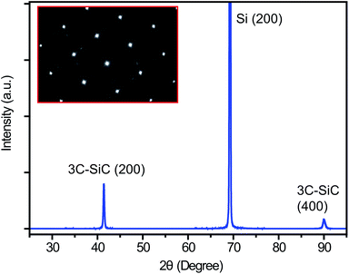 | ||
| Fig. 1 (a) X-ray diffraction pattern of the grown 3C–SiC film on a Si (100) substrate. The inset shows the SAED image. | ||
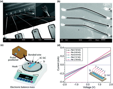
Fig. 2(a) shows an SEM image of the SiC resistors, where the first bond was formed on SiC and the second bond was formed on an external copper-PCB pad. The inset of Fig. 2(a) illustrates an SEM image of the tail of the wire bond formed on the SiC film with a surface area of approximately 50 μm × 50 μm. Fig. 2(b) shows the wire bonding where both first and second bonds were formed on the SiC surface, which can be utilized to interconnect different devices on the same chip. Fig. 2(c) shows the experimental setup to measure the bond strength between the 3C–SiC surface and the Al wires. The pulling force was measured by mounting a bonded SiC/Si chip onto an electronic mass balance (both first and second bonds were connected on the 3C–SiC surface as shown in Fig. 2(b)). Subsequently, a micro-positioner with a hook-tip was employed to pull the center of the wire with each moving step being set at 3 μm. The applied pulling-force was monitored using an electronic balance; the bonding strength was found when the wire started to detach from the SiC surface. Accordingly, the bond strength ranged from 12.6–14.5 mN.
Similarly, for comparison, the bond strength of the directly bonded Al wire on the deposited Al contact of SiC was also measured and it was observed that the strength was in the range of 31.2–38.6 mN, which is 59–62% higher than that between the directly bonded Al wire and the 3C–SiC surface. However, the bond strength between the direct Al wire bonding and the SiC surface is comparable to that of the standard minimum bond pull limit (14.7 mN) of Al wires that are 25 μm in diameter.19
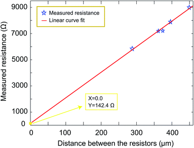
The electrical properties of the bonded wire shown in Fig. 2(d) were then investigated using the Agilent™ U2722A analyzer. The linear behavior of the current–voltage characteristics represents an excellent ohmic contact between the directly bonded Al wires and the 3C–SiC surface, as shown in Fig. 2(d). Furthermore, it is also evident that under a constantly applied voltage, the measured current was found to be inversely proportional to the distance between the bonded pads. Subsequently, the contact resistance between the Al wire and the 3C–SiC film was also measured using a TLM (Transmission Line Measurement) technique and the contact resistivity was found to be approximately 3.32 × 10⁻³ Ω cm2 (Fig. 3).
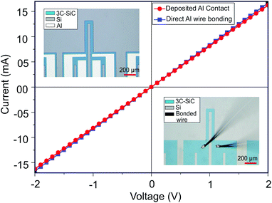
We also compared the resistance of the SiC resistors fabricated using the bonding method to that using the standard one with the metal pad formed by aluminium deposition and etching. The top inset in Fig. 4 shows a SiC resistor with metal electrodes, where an Al layer with a thickness of 300 nm was sputtered using Surrey Nano Systems-γ. From the I–V curve (red line in Fig. 4), the resistance of the SiC with Al electrodes was found to be 1210 kΩ. Subsequently, the deposited Al electrodes were completely removed using TMAH, and the direct wire bonding was performed on SiC, as shown in the bottom inset of Fig. 4. The resistance of the SiC resistor formed using direct wire bonding (solid blue line) was found to be almost the same as that of the SiC resistors with the Al electrode. This indicates the small contact resistance of direct bonding, and also implies the possibility of using this novel method for SiC MEMS applications without the requirement for metal electrodes on SiC.
In addition, to test the feasibility of using direct wire bonding on 3C–SiC devices under high temperature environments, the 3C–SiC film was transferred from the Si substrate onto a glass substrate using an anodic bonding process,1,20 to prevent the leakage through the SiC/Si junction at high temperatures.21,22 The electrical contacts were then prepared by direct wire bonding to the transferred 3C–SiC film. As observed in the I–V characteristics (Fig. 5), the current through the 3C–SiC resistor increased as the temperatures were raised, and the contact between the Al wire and the SiC resistor retained its linear behavior at high temperatures, which is a desired property for applications at elevated temperatures. Furthermore, after cooling down to room temperature, the device showed the same I–V characteristics as under the initial room temperature conditions, demonstrating the repeatable and stable behavior of the device at high temperatures.
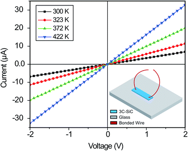 | ||
| Fig. 5 Current–voltage response of a 3C–SiC resistor on a glass substrate at different temperatures. The inset shows a schematic of the 3C–SiC/glass resistor. | ||
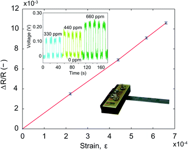
To demonstrate the application of the direct wire bonding method, a SiC strain sensor was developed utilizing the piezoresistive effect. The bottom inset of Fig. 5 shows a SiC on Si cantilever, where the SiC strain sensors were patterned into U-shape structures, as illustrated in the inset of Fig. 4. Direct wire bonding was employed to make contact with the copper PCB placed on the clamp of the SiC/Si cantilever. The piezoresistive effect of the fabricated 3C–SiC resistor was measured using the bending beam method, where the uniaxial stress was induced in the [110] direction.23,24 It was observed that the relative resistance change increased linearly with increasing strain. This is a desirable property for p-type 3C–SiC, as the uniaxial stress was applied in the longitudinal direction, which means that the direction of the current flowing through the resistor and that of the applied stress were the same. Furthermore, the responses showed excellent repeatability at constant strain levels, as shown in the top inset of Fig. 6.
4 Conclusions
In conclusion, this study successfully demonstrated the feasibility of direct wire bonding for 3C–SiC MEMS devices, such as strain sensors for high temperature applications. It is observed experimentally that the bonded wires were physically and electrically stable under stress and high temperature conditions. Direct wire bonding also provides quick and easy access to the electrical properties of a 3C–SiC film just after CVD deposition. In addition, the metallization of SiC MEMS devices with direct Al wire bonding is more cost-effective and time-efficient compared to that of the conventional metallization process, which requires expensive and complicated fabrication processes. Therefore, the study presented here promises an efficient, cost-effective, and mechanically stable wiring technique for 3C–SiC based MEMS devices using direct wire bonding.Conflicts of interest
There are no conflicts to declare.Acknowledgements
This work was performed in part at the Queensland node of the Australian National Fabrication Facility, a company established under the National Collaborative Research Infrastructure Strategy to provide nano- and microfabrication facilities for Australia’s researchers. This work has been partially supported by Griffith University’s New Researcher Grants and Australian Research Council grants LP150100153 and LP160101553.References
- H.-P. Phan, H. H. Cheng, T. Dinh, B. Wood, T.-K. Nguyen, F. Mu, H. Kamble, R. Vadivelu, G. Walker, L. Hold, A. Iacopi, B. Haylock, D. V. Dao, M. Lobino, T. Suga and N.-T. Nguyen, ACS Appl. Mater. Interfaces, 2017, 9, 27365–27371 CrossRef PubMed.
- S. Liu, H. Liu, Z. Huang, M. Fang, Y. G. Liu and X. Wu, RSC Adv., 2016, 6, 24267–24272 RSC.
- D. V. Dao, H.-P. Phan, A. Qamar and T. Dinh, RSC Adv., 2016, 6, 21302–21307 RSC.
- A. Qamar, H.-P. Phan, D. V. Dao, P. Tanner, T. Dinh, L. Wang and S. Dimitrijev, IEEE Electron Device Lett., 2015, 36, 708–710 Search PubMed.
- A. R. M. Foisal, A. Qamar, H.-P. Phan, T. Dinh, T.-K. Nguyen, P. Tanner, E. W. Streed and D. V. Dao, ACS Appl. Mater. Interfaces, 2017, 9, 39921–39925 CrossRef PubMed.
- A. R. M. Foisal, H.-P. Phan, T. Kozeki, T. Dinh, T.-K. Nguyen, A. Qamar, M. Lobino, T. Namazu and D. V. Dao, RSC Adv., 2016, 6, 87124–87127 RSC.
- H.-P. Phan, A. Qamar, D. V. Dao, T. Dinh, L. Wang, J. Han, P. Tanner, S. Dimitrijev and N.-T. Nguyen, RSC Adv., 2015, 5, 56377–56381 RSC.
- H. So and D. G. Senesky, Appl. Surf. Sci., 2016, 387, 280–284 CrossRef.
- Y. Takahashi and M. Inoue, J. Electron. Packag., 2002, 124, 27–36 CrossRef.
- J. Y. Lee, Y. C. Chen and M. S. Lin, Method of wire bonding over active area of a semiconductor circuit, U.S. Pat., 9,142,527, 2015.
- N. Zommer, Solderless die attach to a direct bonded aluminum substrate, U.S. Pat., 8,716,864, 2014.
- B. Gehman, IEEE Trans. Compon., Hybrids, Manuf. Technol., 1980, 3, 375–383 CrossRef.
- G. Harman and J. Albers, IEEE Trans. Parts, Hybrids, Packag., 1977, 13, 406–412 CrossRef.
- H. So and D. G. Senesky, J. Phys. D: Appl. Phys., 2016, 49, 285109 CrossRef.
- L. Wang, S. Dimitrijev, J. Han, P. Tanner, A. Iacopi and L. Hold, J. Cryst. Growth, 2011, 329, 67–70 CrossRef.
- S. A. Kukushkin and A. V. Osipov, J. Phys. D: Appl. Phys., 2014, 47, 313001 CrossRef.
- H.-P. Phan, D. V. Dao, P. Tanner, L. Wang, N.-T. Nguyen, Y. Zhu and S. Dimitrijev, Appl. Phys. Lett., 2014, 104, 111905 CrossRef.
- A. Qamar, H.-P. Phan, J. Han, P. Tanner, T. Dinh, L. Wang, S. Dimitrijev and D. V. Dao, J. Mater. Chem. C, 2015, 3, 8804–8809 RSC.
- Department of Defense, MIL-STD-883E Test Method Standard Microcircuits, Method 2011.7, 1996 Search PubMed.
- C. Tudryn, S. Schweizer, R. Hopkins, L. Hobbs and A. J. Garratt-Reed, J. Electrochem. Soc., 2005, 152, E131–E134 CrossRef.
- M. Placidi, A. Pérez-Tomás, M. Zielinski, P. Godignon, J. Millán, X. Jordà, N. Mestres and G. Abadal, J. Micromech. Microeng., 2010, 20, 115007 CrossRef.
- C.-H. Wu, C. A. Zorman and M. Mehregany, IEEE Sens. J., 2006, 6, 316–324 Search PubMed.
- H.-P. Phan, T. Dinh, T. Kozeki, T.-K. Nguyen, A. Qamar, T. Namazu, N.-T. Nguyen and D. V. Dao, Appl. Phys. Lett., 2016, 109, 123502 CrossRef.
- H.-P. Phan, T.-K. Nguyen, T. Dinh, G. Ina, A. R. Kermany, A. Qamar, J. Han, T. Namazu, R. Maeda, D. V. Dao and N.-T. Nguyen, Appl. Phys. Lett., 2017, 110, 141906 CrossRef.
Footnote |
| † These authors contributed equally to this work. |
| This journal is © The Royal Society of Chemistry 2018 |

