
 Open Access Article
 This Open Access Article is licensed under a Creative Commons Attribution-Non Commercial 3.0 Unported Licence
Large-size and high performance visible-light photodetectors based on two-dimensional hybrid materials SnS/RGO
Renfu Zhuo *,
Shiyong Zuo,
Weiwei Quan,
De Yan,
Baisong Geng,
Jun Wang and
Xuehu Men
*,
Shiyong Zuo,
Weiwei Quan,
De Yan,
Baisong Geng,
Jun Wang and
Xuehu Men
School of Physical Science and Technology, Lanzhou University, Lanzhou, Gansu 730000, China. E-mail: zhuorf@lzu.edu.cn; Tel: +86-931-8912719
First published on 3rd January 2018
Abstract
We report a facile solvothermal method to synthesize two-dimensional hybrid materials consisting of layered SnS nanosheets and reduced graphene oxide (SnS/RGO). Large-size photodetectors with a channel length/width = 2 mm/7 mm are fabricated on Si/SiO2 substrates, showing an excellent photoresponsivity of 0.18 A W−1 under visible-light illumination with a detectivity of 4.18 × 10¹⁰ Jones, as well as fast rise and decay times (τrise = τdecay = 0.4 s). SnS/RGO hybrids are therefore promising candidates for potential applications in optoelectronics and low cost, high performance, and reliable photodetectors.
Introduction
The development of 2-dimensional (2D) graphene and layered metal chalcogenide nanosheets has created extensive interest in photodetection in the past few years because of their high carrier mobility, convenient material fabrication and compatibility with semiconductor electronics.1,2 For photon energy utilization purposes, the optically active materials should not only have high absorption coefficient through the whole solar spectrum, but also have the ability to suppress the fast electron–hole recombinations.3–5 Therefore numerous attempts have been made to combine these 2D nanosheets with semiconductor nanostructures, this kind of hybrid photodetectors achieves ultrahigh responsivity due to the synergism between the strong absorption of semiconducting nanostructures and the extremely fast conduction of carriers within the 2D nanosheets.6–9 These hybrid photodetectors, such as graphene/PbS,6 graphene/ZnO,7 MoS2/PbS,8 SnS2/PbS9 et al. have already demonstrated outstanding performance. Unfortunately, all of them are on the micron scales and the fabrication must undergo extremely complex and precise processes for example, 2D nanosheets synthesized by chemical vapour deposition must transfer onto substrates, 2D nanosheets prepared by exfoliation are all on the micron scales, and photodetectors with micro-size channel length which assembled on substrates must use photolithography, all of which are unfit for large-size device fabrication.SnS is considered to be an excellent material for its layered structural-related semiconducting and optical properties. It has an absorption coefficient near the fundamental absorption edge in the order of 104 cm−1, and it can absorb almost the entire visible and the near-infrared range of the solar spectrum.10–13 In addition, SnS is a low-cost, nontoxic, earth-abundant, and heavy-metal free material for optoelectronic devices, and has shown promising applications in lithium-ion batteries,10 photodetectors11 and photocatalysts.13 Different morphologies of SnS, such as nanoflowers, nanoribbons, nanoparticles and nanoflakes, have been synthesized on the several substrates as large-size SnS films.12–17 The large-size SnS films based photodetectors have been established with high Ilight/Idark ratio, excellent stability and fast rise and decay times. However, their photoresponsivity is still relatively low, almost at the level of mA W−1. Another kind of micro-size single SnS nanoribbon/nanosheet based photodetectors, having also been reported by several groups exhibit relatively high photoresponsivity above the level of A W−1.17–22 But such single SnS nanoribbon/nanosheet based photodetectors are on the micron scales and their fabrication must undergo extremely complex and precise processes, which is not suitable for large-scale applications. Nevertheless, all of these reports show that SnS nanostructures are good candidates for high performance photodetectors.
To the best of our knowledge, SnS/RGO hybrids have rarely been reported as photodetector. Herein, we report a facile solvothermal method to synthesize the SnS/RGO hybrid nanosheets. By drop-casting SnS/RGO hybrid nanosheets on Si/SiO2 substrates as large-size photodetectors, enhanced visible-light photosensitivity is obtained.
Experimental
Preparation of SnS/RGO hybrid nanosheets
Natural graphite powder was oxidized to graphite oxide (GO) by the modified Hummers' method. The SnS/RGO hybrid nanosheets were prepared by a solvothermal route according to previous reports.10 In a typical synthesis of the SnS/RGO hybrid, 20 mg of graphite oxide was dispersed into 30 ml ethylene glycol solution by ultra-sonication for 60 min. Next, 226 mg SnCl2·2H2O (1 mmol) and 210 mg citric acid were added to the solution and then stirred for 60 min. Finally, 2 ml (NH3)2S was added to the solution, which was further stirred for 5 min, and then transferred to a 40 ml Teflon-lined stainless steel autoclave. After heating at 463 K for 18 h and naturally cooled to the room temperature, the black product was filtered and washed several times with deionized water and absolute ethanol, and then dried at 333 K for 24 h to obtain the two dimensional (2D) hybrid SnS/RGO.Characterization
The morphology and structure were observed by transmission electron microscopy (TEM: JEM-2100) operated at 200 kV. The crystal structures of the as-synthesized products were characterized by X-ray diffraction (XRD) on a Philips X'Pert Pro Diffractometer. The Raman spectra were recorded with a Jobin YVON HR800UV Laser Raman spectrometer. The X-ray photoelectron spectroscopy (XPS) data were determined on Thermo Scientific XPS spectrometers.The fabrication of photodetectors
The as-synthesized SnS/RGO hybrid nanosheets were dispersed into toluene and dropped onto Si substrates with 300 nm thick SiO2 layer (1 cm × 1 cm), electrodes of Ag (100 nm) using a metal mask were deposited by DC sputtering to form a channel of L/W = 2 mm/7 mm. The final devices were annealed at 400 K for 2 h with the protection of argon gas in order to remove residues and enhance the metallic contacts. The current–voltage (I–V) characteristics were studied by using a Keithley 4200SCS-CVU semiconductor parameter analyzer. For photodetection, a broadband laser-driven light source (EQ-99, Energetiq) calibrated by an UV-enhanced silicon photodiode provided an incident light, while the current were recorded by a current meter Keithley (2410), an attenuator and a power meter to get different intensities of the incident beam, and the spot effective area was determined to be 0.01 cm2.Results and discussion
The XRD pattern of the SnS/RGO hybrid nanosheets is shown in Fig. 1(a). Clearly, all reflection peaks can be indexed to pure SnS with orthorhombic phase (JCPDS 39-0354). No other peaks were observed in the XRD pattern, indicating that the as-synthesized products were in the pure phase. The (001) peak of GO at around 2θ = 10.2° is absent, which indicates that the present solvothermal reaction not only produces the SnS nanosheets but also simultaneously reduces the GO. Fig. 1(b) shows the Raman spectra of SnS/RGO, with the peak at 213.8 cm−1 which is related to the Ag vibration mode of SnS. Also, two typical carbon peaks are observed: the G band (1592.3 cm−1) and the D band (1349.1 cm−1). As we know, the G band is the response of the in-plane stretching motion of symmetric sp2 C–C bonds, whereas the D band results from the disruption of the symmetrical hexagonal graphitic lattice.10 | ||
| Fig. 1 (a) The XRD patterns; (b) the Raman spectra of the SnS/RGO hybrid nanosheets. | ||
The morphology and microstructure of the as-prepared SnS/RGO hybrids were studied by field emission scanning electron microscopy (SEM) and transmission electron microscopy (TEM). The SEM image in Fig. 2(a) reveals the 2D morphology of the SnS/RGO hybrids. Fig. 2(b) reveals the TEM image of SnS/RGO hybrid nanosheets, it clearly shows curved SnS nanosheets dispersed on large RGO substrates. Fig. 2(c) and (d) display the high-magnification TEM image selected from Fig. 2(b). The SnS shows a well-layered structure, supported on the RGO surface. There are lattice fringes with lattice spacings of 0.28 nm (inset of Fig. 2(d)), corresponding to the (040) plane of SnS.18 Because of the weak van der Waals interaction, SnS shows a well-layered structure with the thickness of 2–10 nm, which indicates that each sheet is composed of 8–40 layers of SnS along the b-axis. This weakly bound interlayer characteristic, the nucleation and the subsequent growth of SnS atoms on the lattice along the b-axis, lead to the formation of the SnS/RGO hybrid nanosheets.18,23
 | ||
| Fig. 2 (a) The SEM image; (b–d) the TEM images of the SnS/RGO hybrid nanosheets. | ||
To further evaluate the SnS/RGO hybrid nanosheets, X-ray photoelectron spectroscopy (XPS) was performed, as shown in Fig. 3(a). The peaks of Sn are shown in Fig. 3(b). It can be seen that the two strong peaks at around 486.6 and 495.0 eV can be attributed to Sn 3d5/2 and 3d3/2 respectively, which agrees well with the reference data of Sn2+ in SnS. No evidence of Sn4+ (binding energy at 485.9 eV) was detected in the spectra.11 The S 2p3/2 at 161.8 eV (Fig. 3(c)) and S 2s1/2 at 223.5 eV are attributed to the binding energies of SnS. In Fig. 3(d), the spectrum C 1s can be deconvoluted into four peaks, which are ascribed to the sp2 bonded carbon (C–C, 284.6 eV and C![[double bond, length as m-dash]](https://www.rsc.org/images/entities/char_e001.gif) C, 285.1), the epoxy/hydroxyl groups (C–O, 286.9 eV) and the carboxyl groups (CO, 289 eV). Under the solvothermal condition, the increased temperature and autogenous pressure led to the reduction of graphene oxide into RGO, but the C–O or CO of the interfacial bonding was still left after the reduction.10,24
C, 285.1), the epoxy/hydroxyl groups (C–O, 286.9 eV) and the carboxyl groups (CO, 289 eV). Under the solvothermal condition, the increased temperature and autogenous pressure led to the reduction of graphene oxide into RGO, but the C–O or CO of the interfacial bonding was still left after the reduction.10,24
 | ||
| Fig. 3 XPS results of SnS/RGO hybrid nanosheets. | ||
The optical image and the schematic of the device of SnS/RGO hybrid nanosheets based photodetector is shown in Fig. 4(a). Fig. 4(b) presents the transfer characteristics (Ids–Vg) of the device with SnS/RGO in the dark and under visible-light illumination (P = 10 mW cm−2, Vds = 5 V), respectively. In comparison, the corresponding transfer curves of the undecorated device with pure RGO are also plotted in Fig. 4(b). All devices exhibit typical n-type semiconducting behaviour. We find that the electrical properties of RGO after SnS decoration become very sensitive to light. To preclude the possibility of intrinsic photoresponses of RGO, we first detect the electrical properties of RGO before SnS decoration when visible light is switched on and off. We don't observe the obvious current changes under light irradiation, which set the foundation for the following studies of the charge transfer at the SnS/RGO interfaces. After SnS decoration, the devices show a slight conductance decrease, most likely due to the scattering effect for carriers created by SnS which are intimately covered on RGO surfaces.25 Noticeably, upon light irradiation, obvious increase in source-drain current (Ids) occurred regardless of the gate bias in the device based on SnS/RGO. Previous studies have demonstrated that the incident visible light generated delocalized electron–hole pairs over the SnS nanosheets.11 The photogenerated holes behave as coulomb traps, the electrons in SnS could penetrate through the interface to the RGO conductive channel, which resulted in the n-type carrier concentration increase in the SnS/RGO hybrid devices. The mobility of the carriers can be calculated by:
 | (1) |
 | ||
| Fig. 4 (a) The optical image and schematic of a representative device. (b) The transfer characteristics (Ids–Vg) of the photodetectors based on RGO and SnS/RGO in the dark and under visible-light illumination, P = 10 mW cm−2. | ||
Fig. 5(a) shows the output characteristics (Ids–Vds) of the photodetector based on RGO and SnS/RGO in dark and under illumination (P = 10 mW cm−2, Vg = 0 V), respectively. The plots show a linear increase of the current with the applied voltage, indicating an ohmic contact between the SnS/RGO and Ag electrodes. In addition, a pronounced increase of the photocurrent under illumination is observed after SnS decoration, suggesting a strong absorption of SnS and effective charge transfer between the SnS decoration and the RGO channel. Fig. 5(b) shows the Ids–Vds curves of the SnS/RGO under illumination with different light intensities. It is found that the conductance and slopes of I–V curves presented monotonic increase according to the light power density, which meant higher sensitivity of the device illuminated by higher power intensity at a higher bias voltage. A higher power intensity and higher voltage can drive photon-generated charge carriers to reach the electrodes faster, suppressing recombination of hole–electron pairs.21,27 This phenomenon suggests that the photocurrent is mainly determined by the amount of photon-generated carriers under illumination.
 | ||
| Fig. 5 (a) Output characteristics Ids–Vds of the photodetectors based on RGO and SnS/RGO in the dark and under visible-light illumination. (b) Ids–Vds curves of SnS/RGO with different light intensities. | ||
In Fig. 6(a), the photocurrent (Iph = Ilight − Idark) of SnS/RGO as a function of the light intensity is plotted, measured at Vds = 5.0 V, Vg = 0 V. It can be seen that the device is very sensitive to the illumination power. By fitting the experimental data, it can be expressed by a power-law equation Iph ∝ P0.68, demonstrating the efficiency of the photogenerated charge carriers.26,28 The performance of the photodetector is generally judged by several parameters, such as the responsivity (R), detectivity (D*), response rate, and stability. Among the above parameters R, defined as the amount of photocurrent generated per unit area per unit illumination intensity, can be given by R = Iph/PS,20 where S is the effective illumination area. According to this formula, a remarkable responsivity about 0.18 A W−1 (P = 0.12 mW cm−2, Vds = 5.0 V, Vg = 0 V) is obtained. This high photoresponsivity may result from the efficient absorption and optimized device configuration. In addition, the dependence of the photoresponsivity on the light power intensity irradiated on the device is depicted in Fig. 6(b). The phenomenon that the responsivity decreases as the light intensity increases is frequently observed in photoconductivity photodetectors. Under high-power illumination, the numbers of photogenerated carriers available for extraction will be reduced, which is caused by the Auger process or the saturation of recombination/trap states that influence the lifetime of the generated carriers.26 Moreover, considering the fact that it is impractical to compare and evaluate directly the responsivity of photodetectors fabricated from other 2D materials, unless the measurements are done under similar environmental conditions. Thus, another important parameter, detectivity, was also investigated. The specific detectivity (D*) defined as a measure of the least detectable radiant power, can be expressed as:28
 | (2) |
 | ||
| Fig. 6 (a) Plot of photocurrent, (b) corresponding responsivity and detectivity of the device versus light intensities, measured at Vds = 5.0 V, Vg = 0 V. | ||
The dependence of the current on time under alternating dark and illumination conditions (100 mW cm−2) with ON/OFF switch cycle of 100 s is shown in Fig. 7(a). The photocurrent increases to a stable value under illumination, and then dramatically decreases to its initial value as the illumination is turned off, thereby showing excellent stability and reproducible characteristics. Ilight/Idark ratio of about 14, a rise time and a decay time both of 0.4 s are obtained, indicating the rapid photoresponse characteristics (Fig. 7(b)).
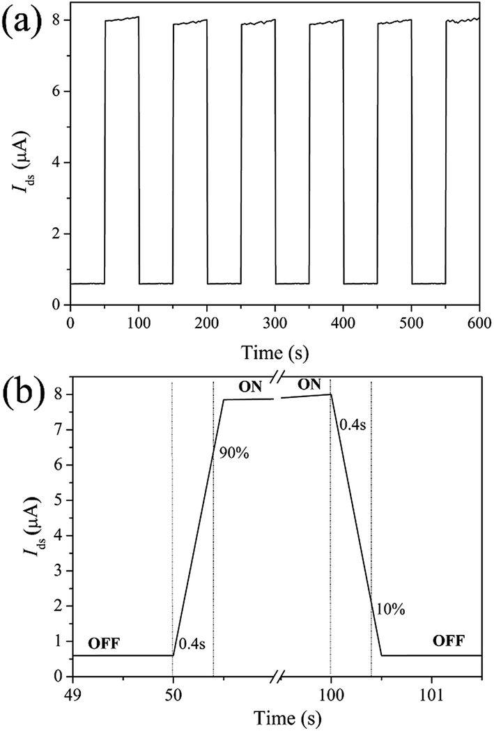 | ||
| Fig. 7 (a) Time response of the SnS/RGO device illuminated with and without light (100 mW cm−2). (b) Rise and decay time. All measured at Vds = 5.0 V, Vg = 0 V. | ||
The performance of the SnS/RGO hybrid nanosheets photodetector in comparison with previously reported large-size SnS film based devices is summarized in Table 1. It is clear that the key parameters of our device are much higher than that of SnS film based large-size photodetectors,12–17 and are also close to that of single SnS nanoribbon/nanosheet based complex micron-size photodetectors.11,18–22 The enhanced photoresponse may be attributed to several reasons. The good ohmic contacts should contribute to a rapid diffusion of the charge carriers, and therefore, accelerate the transportation of carriers and increase the response speed. Furthermore, a large specific surface area of the SnS/RGO nanosheets can promote a fast, effective separation of photocarriers and defer the electron–hole recombinations simultaneously to prolong the photoexcited carrier lifetime, resulting in the high responsivity and detectivity.22 More significantly, the synergism between the strong absorption of SnS and the fast conduction of electrons within the RGO would be beneficial to the separation of electron–hole pairs and thus to the higher photocurrent and faster response rate.9,28
| Large-size SnS film based photodetector | Responsivity [A W−1] | Detectivity [Jones] | Power density [mW cm−2] | Ilight/Idark | Rise/decay time [s] | References |
|---|---|---|---|---|---|---|
| SnS nanoflowers on FTO | 7.05 × 10⁻⁴ | — | 100 | — | 0.5/0.5 | 12 |
| SnS nanoribbons on PET | 8.7 × 10⁻⁴ | — | 100 | 22 | 5.4/1.8 | 13 |
| SnS films on glass | 4.0 × 10⁻⁴ | 7.1 × 10⁷ | 60 | 1.32 | 1.2/3.0 | 14 |
| SnS nanoflakes on PET | 4.0 × 10⁻⁶ | — | 25 | 14 | 0.53/0.5 | 15 |
| SnS nanoparticles on Si/SiO2 | 1.7 × 10⁻³ | — | 50 | 1.2 | 0.45/0.56 | 16 |
| SnS nanoflakes on glass | — | — | 38 | 8 | 0.44/0.5 | 17 |
| SnS/RGO hybrid nanosheets on Si/SiO2 | 0.18 | 4.18 × 10¹⁰ | 0.12 | 1.4 | 0.4/0.4 | This work |
Conclusions
In summary, a simple solvothermal procedure is demonstrated to prepare SnS/RGO hybrid nanosheets. The large-size photodetectors based on the nanocomposites exhibits an excellent photoresponsivity of 0.18 A W−1 under visible-light illumination with a detectivity of 4.18 × 10¹⁰ Jones. The SnS/RGO hybrids thus show promising potential for cost effective, environmental friendly, less toxic, and naturally occurring optical, electronic, and optoelectronic devices.Conflicts of interest
There are no conflicts to declare.Acknowledgements
This work was supported by the Natural Science Foundation for Young Scientists of Gansu Province, China (Grant No. 1506RJYA220), the National Natural Science Foundation of China (Grant No. 51335010), the Fundamental Research Funds for the Central University (lzujbky-2017-175 and lzujbky-2016-116), the Lanzhou Chengguan District Scientific Reaserch Foundation (cgkj2015-5-1).Notes and references
- A. Ferrari, F. Bonaccorso, V. Fal'ko, K. Novoselov and S. Roche, et al., Nanoscale, 2015, 7, 4598–4810 RSC.
- H. Chen, H. Liu, Z. Zhang, K. Hu and X. Fang, Adv. Mater., 2016, 28, 403–433 CrossRef CAS PubMed.
- K. Hu, H. Chen, M. Jiang, F. Teng, L. Zheng and X. Fang, Adv. Funct. Mater., 2016, 26, 6641–6648 CrossRef CAS.
- X. Fang, L. Hu, K. Huo, B. Gao, L. Zhao, M. Liao, P. K. Chu, Y. Bando and D. Golberg, Adv. Funct. Mater., 2011, 21, 3907–3915 CrossRef CAS.
- J. Chao, S. Xing, Z. Liu, X. Zhang, Y. Zhao, L. Zhao and Q. Fan, Mater. Res. Bull., 2018, 98, 194–199 CrossRef CAS.
- Z. Sun, Z. Liu, J. Li, G. Tai and S. Lau, Adv. Mater., 2012, 24, 5878–5883 CrossRef CAS PubMed.
- D. Son, B. Kwon, D. Park, W. Seo, Y. Yi, B. Angadi, C. Lee and W. Choi, Nat. Nanotechnol., 2012, 7, 465–471 CrossRef CAS PubMed.
- D. Kufer, I. Nikitskiy, T. Lasanta, G. Navickaite and F. Koppens, Adv. Mater., 2015, 27, 176–180 CrossRef CAS PubMed.
- L. Gao, C. Chen, K. Zeng, C. Ge, D. Yang, H. Song and J. Tang, Light: Sci. Appl., 2016, 5, e16126 CrossRef CAS.
- S. Li, J. Zheng, S. Zuo, Z. Wu, P. Yan and F. Pan, RSC Adv., 2015, 5, 46941–46946 RSC.
- Z. Deng, D. Cao, J. He, S. Lin, S. M. Lindsay and Y. Liu, ACS Nano, 2012, 6, 6197 CrossRef CAS PubMed.
- J. Chao, Z. Xie, X. B. Duan, Y. Dong, Z. R. Wang, J. Xu, B. Liang, B. Shan, J. H. Ye, Di Chen and G. Z. Shen, CrystEngComm, 2012, 14, 3163 RSC.
- J. Chao, Z. Wang, X. Xu, Q. Xiang, W. Song, G. Chen, J. Hu and D. Chen, RSC Adv., 2013, 3, 2746–2753 RSC.
- T. S. Reddy and M. C. S. Kumar, RSC Adv., 2016, 6, 95680–95692 RSC.
- M. S. Mahdi, K. Ibrahim, A. Hmood, N. M. Ahmed, S. A. Azzez and F. I. Mustafa, RSC Adv., 2016, 6, 114980–114988 RSC.
- F. Lu, J. Yang, R. Li, N. Huo, Y. Li, Z. Wei and J. Li, J. Mater. Chem. C, 2015, 3, 1397–1402 RSC.
- M. S. Mahdi, K. Ibrahim, A. Hmood, N. M. Ahmed, F. I. Mustafa and S. A. Azzez, Mater. Lett., 2017, 200, 10–13 CrossRef CAS.
- J. Wang, G. Lian, Z. Xu, C. Fu, Z. Lin, L. Li, Q. Wang, D. Cui and C. Wong, ACS Appl. Mater. Interfaces, 2016, 8, 9545–9551 CAS.
- X. Zhou, Q. Zhang, L. Gan, H. Li, J. Xiong and T. Zhai, Adv. Sci., 2016, 3, 1600177 CrossRef PubMed.
- X. Zhou, L. Gan, Q. Zhang, X. Xiong, H. Li, Z. Zhong, J. Han and T. Zhai, J. Mater. Chem. C, 2016, 4, 2111–2116 RSC.
- J. Xia, D. Zhu, X. Li, L. Wang, L. Tian, J. Li, J. Wang, X. Huang and X. Meng, Adv. Funct. Mater., 2016, 26, 4673–4679 CrossRef CAS.
- Z. Jia, S. Li, J. Xiang, F. Wen, X. Bao, S. Feng, R. Yang and Z. Liu, Nanoscale, 2017, 9, 1916–1924 RSC.
- S. S. Shinde, A. Sami, D. Kim and J. Lee, Chem. Commun., 2015, 51, 15716–15719 RSC.
- X. An, J. C. Yu and J. Tang, J. Mater. Chem. A, 2014, 2, 1000–1005 CAS.
- D. Zhang, L. Gan, Y. Cao, Q. Wang, L. Qi and X. Guo, Adv. Mater., 2012, 24, 2715–2720 CrossRef CAS PubMed.
- P. Yu, X. Yu, W. Lu, H. Lin, L. Sun, K. Du, F. Liu, W. Fu, Q. Zeng, Z. Shen, C. Jin, Q. Wang and Z. Liu, Adv. Funct. Mater., 2016, 26, 137–145 CrossRef CAS.
- Y. Fu, G. Gou, X. Wang, Y. Chen, Q. Wan, J. Sun, S. Xiao, H. Huang, J. Yang and G. Dai, Appl. Phys. A, 2017, 123, 299 CrossRef.
- X. Zhou, Q. Zhang, L. Gan, H. Li and T. Zhai, Adv. Funct. Mater., 2016, 26, 4405–4413 CrossRef CAS.
| This journal is © The Royal Society of Chemistry 2018 |