
CVD growth of continuous and spatially uniform single layer graphene across the grain boundary of preferred (111) oriented copper processed by sequential melting–resolidification–recrystallization
Indu
Sharma
,
Sanjay R.
Dhakate
and
Kiran M.
Subhedar
 *
*
Advanced Carbon Products, Division of Advanced Materials and Devices, Academy of Scientific and Innovative Research (AcSIR)-NPL, CSIR-National Physical Laboratory (NPL), New Delhi-12, India. E-mail: kmsubhedar@gmail.com; kms@nplindia.org; Tel: +91-11-45721090
First published on 9th April 2018
Abstract
The properties of the catalyst used for CVD growth have a significant influence on the quality of the graphene grown. Single crystallinity or preferred (111) orientation with a smooth surface is the most essential criterion for the growth of high quality graphene on a copper substrate. Herein, the effective strategy of pre-heat treatment of the copper substrate for the growth of improved quality single layer graphene is demonstrated. The sequential melting, resolidification and recrystallization with a controlled slow cooling rate leads to preferred (111) oriented grain growth in the copper substrate, which was confirmed with XRD studies. The grain growth evolution and strain relaxation, correlated with surface smoothening, were inferred from AFM studies. The Raman spectroscopy measurement signifies the improved quality of the CVD grown graphene which is almost free from the multilayer patches that are usually associated with the routine CVD growth process. The Raman mapping carried out directly on the graphene/copper surface reveals spatial continuity and uniformity of graphene quality across the copper grain boundaries over a large area, which signifies the importance of the strain relaxed improved surface morphology with a uniform catalytic and crystallographic environment of the underlying surface. The electrical characterization corroborates the result of improved quality of graphene grown on recrystallized copper. Hence, a feasible process of high quality graphene growth was achieved with a simple but effective strategy of preheat treatment involving melting, resolidification and recrystallization of the copper substrate.
Introduction
Since the discovery of single layer graphene with extraordinary properties,1–3 the technological developments in the synthesis of graphene have evolved from trial and hit based micromechanical exfoliation to large scale chemical vapour deposition (CVD) based techniques. Amongst these, the CVD growth of graphene on a copper substrate is the most consistent, easily controllable and more importantly scalable technique.4–7 However, until now the quality of the CVD grown graphene has not matched that of micromechanically exfoliated graphene. The electronic and mechanical properties of exfoliated graphene are far better than those of CVD grown graphene.8–11 The comparatively inferior properties of CVD grown graphene are usually attributed to the presence of crystalline defects and mechanical deformations in the graphene layer.12,13 The properties of the copper catalyst such as its surface morphology, crystallographic structure and microscopic orientation, have a pronounced influence on the carrier mobility, grain boundaries etc. of the CVD grown graphene. The surface roughness of the underlying copper significantly contributes to the quality of the graphene.14–16 The crystallographic orientations of the copper substrate have a pivotal role in the CVD growth of graphene. The (111) plane of FCC copper was found to produce the best single layer graphene because of several reasons, such as the fact that it minimizes the free energy and maintains a hexagonal symmetry with minimum lattice mismatch with graphene.17–20 Hence, it is very much essential to use either a single crystalline or preferred (111) oriented copper substrate for the CVD growth of graphene, both of which are very costly for a scalable CVD process. However, the most widely used cheap and commercially available cold worked copper foils are polycrystalline in nature with poor crystallinity and with very high induced strain. Chemical or electropolishing and annealing can solve the problem of surface roughness and crystallinity only to some extent because polishing can achieve the mere smoothening of the surface, but it is ineffective in removing the induced strain which is associated with a cold rolling process. The annealing process can induce grain growth which is again limited by the size of the grain and its orientation.21,22 The other approaches which have been adopted so far to get desirable and preferred Cu(111) orientation and CVD growth of high quality graphene include the annealing of copper in the presence of hydrogen or carrying out the CVD growth on a melted copper substrate, which yields a high quality sample.23,24 However, in the former approach the change in crystallographic orientation of copper to the desired (111) orientation is favored by removal of the surface copper oxide layer with the aid of annealing in the presence of hydrogen. The said recrystallization has been carried out without melting of the available copper, which might not remove all surface irregularities, and there might not be an ultra smooth surface which is required to reduce the nucleation density, an essential condition for growth of high quality graphene, and also there could be the presence of remnant strain, which was induced during the manufacturing process of the foil and may again influence the quality of the CVD grown graphene. In the later approach the CVD growth of single layer graphene on melted copper is no more a self limiting process as the copper evaporates severely at and above its melting point making the Cu surface very unstable and also the generated copper vapors contribute to an excess of carbon adatoms which could result in the growth of bilayer or multilayer graphene. Hence, a more feasible and suitable approach for high quality graphene growth by CVD should be sequentially to recrystallize the commercially available copper substrate into a preferred oriented (111) substrate by melting and subsequently to grow single layer graphene at optimum growth temperature instead of growing it on melted copper.In light of this, in the present investigation, a single step process for CVD growth of improved quality graphene on a preferred (111) orientated smooth and recrystallized copper substrate processed by high temperature heat treatment of commercially available coarsely crystalline copper foil has been demonstrated. A simple and effective approach of sequential melting, resolidification and recrystallization of commercially available copper was employed which produces Cu(111). XRD and AFM studies were carried out to understand the crystallographic orientation, surface roughness and related strain relaxation of the copper substrate. The quality of the graphene was studied using Raman spectroscopy. The Raman mapping technique was utilized to understand the uniformity and spatial properties of the graphene across the copper grain boundaries.
Experimental section
The growth of graphene was carried out on 25 μm thick copper foil (99.8% pure, Alfa Aesar #13382). The foil was thoroughly cleaned with acetone, acetic acid, DI water and IPA. The copper foil was placed inside a quartz reactor in the isothermal zone of a custom built thermal CVD system and evacuated, filled with argon and again pumped down to 0.005 mbar, then heated further under hydrogen flow of 12 sccm at a pressure of 0.18 mbar. Prior to graphene growth the copper foil was sequentially heat treated for melting, resolidification and recrystallization of the copper substrate and finally CVD growth was carried out at 1045 °C. In other experiments the foil was only annealed at different tempratures from 980 to 1050 °C to study the effect of annealing temperature on the average grain size. The average grain size was estimated with the Average Grain Intercept (AGI) method using optical microscope images. In this method, the grain or domain size for a given material is quantified by drawing a set of randomly positioned line segments on the micrograph, counting the number of times each line segment intersects a grain boundary, and finding the ratio of intercepts to line length. For the growth of graphene at 1045 °C, methane was introduced with a flow rate of 4 sccm for an initial time period of 3 minutes followed by an increase in its flow rate to 25 sccm with a total growth time of 30 minutes. After growth the samples were cooled down to 100 °C. Methane flow was turned off at 650 °C and hydrogen flow below 100 °C. Finally, the as grown graphene was transferred onto a silicon oxide substrate using our established procedure.25 An optical microscope (Zeiss Axiolab A1) was used to study the grain growth and estimate the size of the grains of the copper substrate. X-ray diffraction (XRD) was performed using the Rigaku Diffractometer with CuKα radiation (λ = 1.54 Å). Surface morphology was studied using an Atomic Force Microscope (AFM, Multimode-V Veeco) and surface roughness was analysed with Research Nanoscope-7.20 software. The micro-Raman mapping was performed under ambient conditions with a Renishaw InVia Raman microscope equipped with a 514 nm (2.41 eV) wavelength excitation laser and 2400 lines per mm grating. A laser beam size of ∼1 μm with a ×50 objective lens was used. The electrical contact pads were deposited on the graphene on the Si/SiO2 substrate by thermal evaporation of Au using a physical shadow masking technique. The electrical current–voltage chatactristics were measured using the two probe method with a Kiethely source meter.Results and discussion
To improve the quality of the graphene growth by CVD, the effect of annealing of the copper substrate on its crystallinity was studied. Fig. 1 shows the surface morphology of the copper substrate as received, and the samples preheat treated at 1000 and 1050 °C and resolidified and recrystallized. These samples are referred to as T0, T1000, T1050 and TRSC respectively. The ‘as received’ sample does not show any visible domains of copper and only shows the processing lines resulting from a cold rolling process. However, the annealed samples show grain growth of copper. The grain size increases systematically with an increase in annealing temperature from 980 to 1060 °C. The variation of the average grain size as a function of inverse temperature is shown in Fig. 2. The observed linear relationship clearly indicates that the annealing induced grain growth is a consequence of a temperature activated diffusion process. The temperature dependent reaction rate is governed by the Arrhenius equation, | (1) |
 | ||
| Fig. 1 Optical images of (a) the as-received copper foil (T0), the samples annealed at (b) 1000 °C (T1000) and (c) 1050 °C (T1050), and (d) the resolidified and recrystallized sample (TRSC) (scale bar-50 μm). | ||
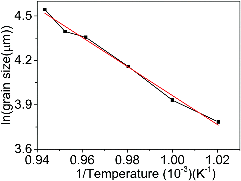 | ||
| Fig. 2 Arrhenius plot for variation of average grain size as a function of inverse temperature. | ||
The activation energy according to eqn (1) extracted for the annealing induced grain growth process was found to be 0.845 eV which is considerably lower than the corresponding value for bulk copper (1.28 eV).26 The possible reason for the obtained lower values of activation energy could be the strain originating from grain boundaries. Indeed the cold rolling in a foil manufacturing process induces high strain in the foil and in the present case it is found that even high temperature annealing could not to reduce the strain in the foil significantly.
To investigate further, prior to growth of graphene the Cu substrate was heated to 1080 °C which is very close to its melting point (1084.6 °C). At this temperature the copper is in a semi-molten state but not in a complete liquid state. Further small increase in the temperature leads to complete melting of copper and its ball formation takes place because of its dewetting with the supporting quartz plate on which the foil is rested during heat treatment. The copper foil was kept there at 1080 °C for 10 min and then cooled down to 1000 °C for its resolidification and recrystallization. X-ray diffraction (XRD) was carried out for samples with different heat treatment processes. Fig. 3 shows the XRD pattern of the as-received (T0) copper foil, the annealed samples T1000 and T1050, and the resolidified and recrystallized sample (TRSC). The T0 and other annealed samples show a dominant (002) peak along with small intensity (111) and (220) peaks. However, the TRSC sample shows only the (111) peak implying that the melting and subsequent resolidification of the copper substrate leads to recrystallization of the copper foil. The XRD patterns of the recrystallized copper consistently show a single peak of (111) with complete suppression of peaks of other planes which are otherwise present before recrystallization. In order to confirm spatial variations of the crystallographic structure the same sample was measured a few times such that the data is collected from different areas of the sample. The results of these measurements on the same sample and also in different samples recrystallized with similar pre-treatment conditions show consistent results and confirm the formation of preferred oriented copper (111). It is noteworthy to mention that the solidification was carried out with slow cooling (with rate less than 3 °C per minute) which could have resulted in the complete recrystallization of copper. Interestingly the recrystallization comes up with preferred (111) oriented domains. The Cu generally crystallizes in the simple FCC crystal structure, where the low index (100), (110), and (111) surfaces have the lowest surface energy. Furthermore, Robinson et al.27 have reported that the Cu(111) orientation has a lower surface energy among the lower index crystalline surface. Secondly, the dewetting of copper in a molten state during heat treatment is very crucial as the weaker interaction of the foil with the supporting quartz plate leads to minimization of interfacial energy. Usually for the grain growth there exist grain orientation specific driving forces. The top and bottom surface of the foil are associated with the excess free energy γs. The bottom surface will have additional excess free energy γi arising from its interface with the supporting quartz plate. Both γs (the energy of the free surface) and γi depend strongly on the orientation of the grain with respect to the plane of the foil. Typically, for FCC metals on amorphous substrates like quartz or fused silica, both γs and γi are minimized for grains with (111) texture, implying that growth of grains with (111) texture is generally preferred over growth of grains with other orientations.28 This can result in the development of bimodal grain size distributions,29 in which the large grains have γs and γi minimizing orientations. Furthermore, large grains consume all other grains, resulting in a population of grains with a monomodal size distribution which here is the preferred (111) orientation of copper grains with respect to the plane of the foil. This recrystallization of copper with preferred (111) orientation is very crucial for further growth of graphene by the CVD technique.
 | ||
| Fig. 3 XRD pattern of the as-received (T0) copper foil, the annealed samples T-1000 and T-1050, and the resolidified and recrystallized sample (TRSC). | ||
The induced strain in the material has a pronounced effect on its surface morphology and the signatures of the strain relaxation can be easily seen from surface roughness variations. Fig. 4 shows atomic force microscope (AFM) images of the as-received (T0) copper foil, annealed samples T-1000 and T-1050 and the resolidified and recrystallized sample (TRSC). The morphology of the ‘as received’ sample shows grooves on the surface which were also observed from optical images. The T-1000 and T-1050 samples show an improvement in surface morphology with decreasing surface roughness. The AFM image of TRSC shows a very flat and smooth surface as a consequence of melting and resolidification of the copper foil. The average surface roughness (Ra) and root mean square surface roughness (Rq) estimated for T0, T-1000, T-1050 and TRSC are tabulated in Table 1. The surface roughness values were found to decrease more drastically for the resolidified and recrystallized sample (Ra from 56.7 to 1.4 nm) compared to the other annealed samples indicating significant relaxation of the induced strain in the foil. The observed correlation of surface roughness with induced strain is consistent with earlier studies.30,31 The employed sequence of resolidification and recrystallization of the copper substrate leads to strain relaxation with a smooth surface and preferred (111) oriented grain growth. Here getting the strain relaxed smooth surface of the resolidified and recrystallized copper substrate is the other critical and important aspect which further contributes for a better quality of CVD grown single layer graphene because the smooth surface with reduced edges and enhanced terraces reduces the nucleation density and leads to the growth of graphene with less grain boundary effects.32–34
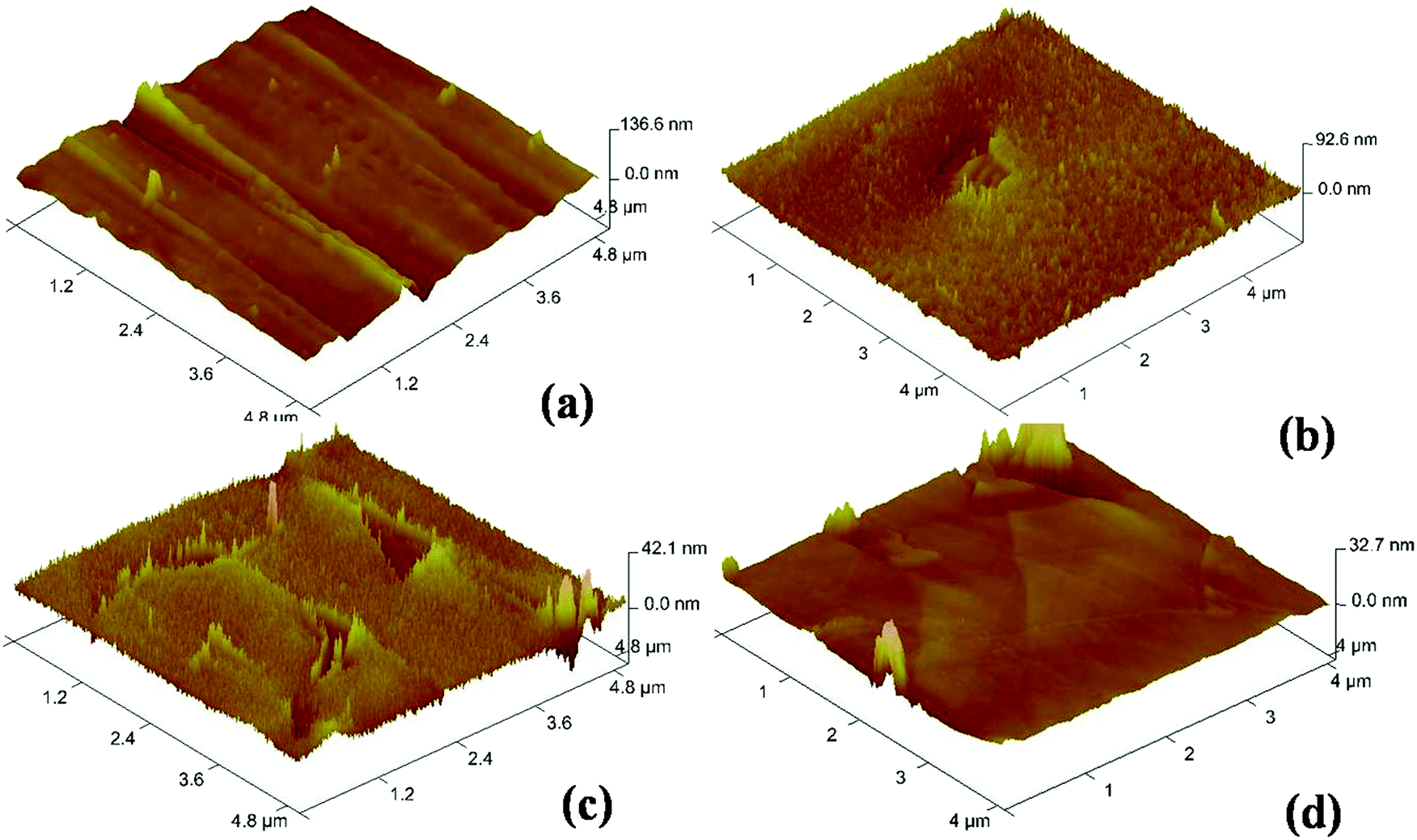 | ||
| Fig. 4 Atomic force microscope (AFM) images of (a) the as-received (T0) copper foil, the annealed samples (b) T-1000 and (c) T-1050, and (d) the resolidified and recrystallized sample (TRSC). | ||
| Sample | R a (nm) | R q (nm) |
|---|---|---|
| T0 | 56.7 | 69.4 |
| T-1000 | 39.9 | 47.6 |
| T-1050 | 11.2 | 14.8 |
| TRSC | 1.44 | 3.17 |
The precondition of the copper substrate like its grain size and crystallographic orientation, crystallinity, and surface morphology has pronounced effects on the properties of CVD grown graphene. The Cu(111) plane produces graphene with superior quality, with fewer defects and minimal coverage of multilayer patches and having a high coverage of a single layer.17,19 Hence, the resolidification and recrystallization process which results in strain relaxed Cu(111) orientation with a smooth surface which is very much crucial for the growth of high quality graphene on commercially available copper foil and hence the process was further used to preheat treat the Cu substrate prior to the CVD growth of graphene.
The CVD growth of graphene is reported in a wide window of temperatures ranging from 850 to 1090 °C. Though the higher growth temperature produces better graphene, the CVD growth process at very high temperature leads to a higher fraction of multilayer regions because at a high temperature around its melting point the evaporation rate of Cu is very high even in a high or atmospheric pressure CVD growth process and the catalytic activity of the resulting copper in the vapor phase contributes to multilayer graphene. In our low pressure CVD growth process, we tried to grow the graphene on melted copper at 1080 °C which leads to the growth of a discontinuous graphene layer or patches which are again of multilayer nature because of the catalytic activity of copper vapors and extremely unstable copper surface as a result of severe evaporation of copper atoms at this high temperature and low growth pressure. Hence, prior to growth of graphene and after melting at 1080 °C, the Cu substrate was slowly cooled down to 1000 °C (TS) and stabilized at this temperature for ten minutes and again increased to its growth temperature, TG of 1045 °C and CVD growth was carried out. The melting followed by slow cooling resulting in recrystallization which is very much crucial for getting uniform single layer graphene of high quality. The employed growth scheme is as shown in Fig. 5. Here, in addition to preferred orientation of the Cu substrate and its surface improvement, the sequence of melting, resolidification and recrystallization is also very much important for the actual CVD process for high quality graphene growth. There are other reported methods35,36 to produce monocrystalline Cu(111) in which the Cu foil is either annealed for a long time of about 12 hours at annealing temperature or the starting Cu foil is chemically polished and then annealed at a temperature below its melting point and the process is repeated several times so as to get a single (111) domain. This makes the whole process as time and energy consuming. Furthermore, the process is prone to contamination because of the involved chemical treatment or long duration of the process. In contrast the present work demonstrates a fast process which produces a copper domain with a preferred orientation of (111) although with a limited size. However, interestingly during CVD growth on this preferred oriented copper substrate, the single layer graphene grows without any impediment across the domain boundary of preferred oriented Cu(111). The spatial uniformity of graphene quality across the Cu(111) domain was then further confirmed with Raman mapping.
 | ||
| Fig. 5 Schematic of the stepwise process employed for CVD growth of graphene with melting, resolidification and recrystallization. | ||
Different characterization techniques are being used to judge the quality of graphene. Raman spectroscopy is the best and most commonly used technique to decide the ultimate quality of the graphene on the basis of induced defects, number of layers, doping of impurities and even incorporated strain etc. In Raman spectroscopy the quality of the graphene is judged from evaluation of different parameters such as peak position, peak width (FWHM) and relative ratios of the intensity for the G, 2D and D peaks.37,38 The stress in the sample can lead to a red or blue shift in the position of the 2D peak depending upon the nature of the strain like compressive or tensile. Charge carrier doping also shows similar effects. The intensity ratios ID/IG and I2D/IG are the measures used for determining the quality of a single layer of graphene. The Raman mapping of these quantities gives the spatial uniformity of the graphene quality. Fig. 6 shows (a) Raman spectra of CVD grown single layer graphene on the Si/SiO2 substrate with a prior process of resolidification and recrystallization (the inset of the figure shows the corresponding image) and its corresponding Raman mapping images for peak intensity ratios (b) ID/IG and (c) I2D/IG, (d) 2D peak FWHM (cm−1) and (e) 2D peak position (cm−1). The I2D/IG and ID/IG ratios derived from D, G and 2D peak mapping are around 3.2 and 0.1 respectively indicating the superior quality of the CVD grown graphene. The average of the I2D/IG and ID/IG ratios taken for a number of samples is about 3 and 0.1 respectively showing reproducibility of the process. Furthermore, the 2D peak has a FWHM of about 29 cm−1 usually about the same for exfoliated graphene indicating the high quality of the CVD grown single layer graphene. The position of the 2D peak is at 2685 cm−1 and without any energy shift in the Raman shift again indicating the graphene without doping or induced strain. The variation of colour contrast in the optical micrograph of the graphene transferred onto the Si/SiO2 wafer can be used to distinguish the single layer and multilayer graphene easily39 and this concept is used to estimate the percentage of single layer coverage over a large area, which in the case of the recrystallized sample is about 98%.
 | ||
| Fig. 6 (a) Raman spectra of CVD grown single layer graphene on the Si/SiO2 substrate with a prior process of resolidification and recrystallization (the inset is the corresponding photograph) and its corresponding Raman mapping images for peak intensity ratios (b) ID/IG and (c) I2D/IG, (d) 2D peak FWHM (cm−1) and (e) 2D peak position (cm−1) (the area selected for mapping is 10 by 10 μm). | ||
Furthermore, to understand the quality of graphene with respect to the copper grains on which it is grown and its uniformity across the grain boundaries, Raman mapping was carried out directly on the graphene/copper surface to reveal the spatial continuity and uniformity of the graphene properties across the copper grain boundary. The ID/IG and I2D/IG ratios are used for determining the quality of graphene which in turn are influenced by the properties of the copper surface such as its roughness and its crystallographic orientations. Hence, the difference in grain orientation or difference in their nature and density of defects and smoothness is expected to get reflected in the measured properties of graphene across the grain boundaries of copper. Moreover, the grain boundary associated with such graphene gives significant D peak intensity.13 Hence, the presence of graphene grain boundaries is expected to show its signatures in the Raman mapping. Fig. 7 shows (a) an optical image of graphene on copper across the grain boundary area in which Raman mapping (red shaded area) was carried out and (b) its Raman spectra, and the mapping of intensity ratios (c) ID/IG and (d) I2D/IG derived from Raman mapping of G, 2D and D peaks for CVD graphene grown on a resolidified and recrystallized copper substrate across the grain boundary. The mapping of ID/IG and I2D/IG ratios does not show any abrupt variation or discontinuity across the copper grain boundary implying that the underlying copper surface of different grains provides a consistent environment for the CVD growth of the continuous and uniform single layer graphene without grain boundaries across the copper grain boundary. This indicates that the neighboring grains have uniform crystallographic properties in terms of their surface roughness and related strain, catalytic properties and defects which are mainly controlled by crystallographic orientations. This evidentially confirms the growth of high quality uniform single layer graphene which was supported by the XRD and AFM results again confirming strain relaxed, smooth surface and preferred orientation of (111) copper grains by resolidification and recrystallization of the copper substrate.
 | ||
| Fig. 7 (a) Optical image of graphene on copper across the grain boundary area which is selected for Raman mapping (red shaded area) and (b) its Raman spectra. The intensity ratios (c) ID/IG and (d) I2D/IG derived from Raman mapping of the G, 2D and D peaks for the CVD graphene grown on a resolidified and recrystallized copper substrate across the grain boundary (the area selected for mapping is 10 by 12 μm). | ||
Finally, the electrical measurements on CVD graphene grown on the resolidified and recrystallized copper substrate were carried out. Fig. 8 shows the plot of the current–voltage (I–V) characteristics of CVD grown graphene transferred onto a Si/SiO2 (300 nm) substrate. The measured current–voltage (I–V) characteristics using a two-probe method give a graphene resistance value of 1.6 kΩ. This observed value of resistance is consistent with values reported in the literature.40,41 Moreover, the measured value in the present investigation was obtained from the two probe measurement method which also includes the contact resistance of the electrical contacts to graphene in addition to the graphene resistance. Hence, the actual resistance of the graphene should be less than the measured value of 1.6 kΩ. An empirical relation between carrier mobility (μ) and full width at half maxima (FWHM) of the 2D peak (Γ2D) has been developed based on measured data of carrier mobility and different parameters in Raman spectroscopy for five types of CVD graphene prepared using different catalysts, feed gases, and CVD methods.42 Based on this analysis they found that the FWHM of the 2D peak was closely related to the carrier mobility regardless the type of graphene. In particular, the logarithmic value of the mobility due to long-range scattering shows a linear relationship with the FWHM of the 2D peak as follows,
log![[thin space (1/6-em)]](https://www.rsc.org/images/entities/char_2009.gif) μ = α + β·Γ2D μ = α + β·Γ2D | (2) |
| logμ = 12.157 − 0.116·Γ2D | (3) |
 | ||
| Fig. 8 Current–voltage (I–V) characteristics of CVD graphene grown on a resolidified and recrystallized copper substrate. | ||
In the present investigation the estimated carrier mobility (μ) of the CVD graphene grown on the recrystallized copper substrate using eqn (3) was found to be 6580 cm2 V−1 s−1 for the measured 2D peak FWHM (Γ2D) of about 29 cm−1 for graphene on the SiO2 substrate. This estimated value of carrier mobility is reasonably superior compared to other reported CVD grown graphene samples. Moreover, the obtained carrier mobility is comparable to the mechanically exfoliated samples which are generally supposed to be of the best quality. This proves the worth of the very much essential process of melting–resolidification–recrystallization of the copper substrate for producing high quality graphene by the CVD technique.
Conclusions
An effective strategy of preheat treatment of a copper substrate for the growth of improved quality single layer graphene is demonstrated. The sequential melting, resolidification and recrystallization with a controlled cooling rate leads to preferred (111) oriented grain growth in the copper substrate and was confirmed with XRD studies. The possible reason for the preferred (111) oriented grain growth in copper is the low surface energy of the lower index (111) plane and minimization of interfacial energy resulting from weak interaction of the FCC copper surface with the quartz substrate. The grain growth evolution and strain relaxation with surface smoothening was inferred from AFM studies. The Raman spectroscopy measurement signifies improved quality of the CVD grown graphene which is almost free from the multilayer patches that are associated with the usual CVD growth process. The Raman mapping carried out directly on the graphene/copper surface reveals spatial continuity and uniformity of the graphene quality across the copper grain boundaries, which confirmed the results of surface improvement with a uniform catalytic and crystallographic environment of the underlying surface. It signifies the importance of the employed pre-treatment of melting, resolidification and recrystallization which leads to a single step and feasible CVD process for high quality continuous graphene growth with a simple but effective strategy. The electrical characterization and estimated high carrier mobility corroborates the high quality of the CVD grown graphene on the recrystallized copper substrate. The present study will advance the understanding about the relevance of the structure and surface properties of the copper substrate for the quality of the graphene grown and will help to establish a better CVD process for growth of improved quality single layer graphene, which is still a challenging task.Conflicts of interest
There are no conflicts to declare.Acknowledgements
The authors are thankful to CSIR for supporting this work. One of the authors IS is thankful to CSIR for giving CSIR-SRF. The authors are thankful to Sandip Singh for his help in AFM measurements.References
- K. S. Novoselov, A. K. Geim, S. V. Morozov, D. Jiang, Y. Zhang, S. V. Dubonos, I. V. Grigorieva and A. A. Firsov, Science, 2004, 306, 666–669 CrossRef CAS PubMed.
- K. S. Novoselov, A. K. Geim, S. Morozov, D. Jiang, M. Katsnelson, I. Grigorieva, S. Dubonos and A. A. Firsov, Nature, 2005, 438, 197–200 CrossRef CAS PubMed.
- A. K. Geim and K. S. Novoselov, Nat. Mater., 2007, 6, 183–191 CrossRef CAS PubMed.
- X. Li, W. Cai, J. An, S. Kim, J. Nah, D. Yang, R. Piner, A. Velamakanni, I. Jung, E. Tutuc, S. K. Banerjee, L. Colombo and R. S. Ruoff, Science, 2009, 324, 1312–1314 CrossRef CAS PubMed.
- X. Li, C. W. Magnuson, A. Venugopal, R. M. Tromp, J. B. Hannon, E. M. Vogel, L. Colombo and R. S. Ruoff, J. Am. Chem. Soc., 2011, 133, 2816–2819 CrossRef CAS PubMed.
- S. Bae, H. Kim, Y. Lee, X. Xu, J.-S. Park, Y. Zheng, J. Balakrishnan, T. Lei, H. R. Kim and Y. I. Song, Nat. Nanotechnol., 2010, 5, 574–578 CrossRef CAS PubMed.
- Z. Yan, J. Lin, Z. Peng, Z. Sun, Y. Zhu, L. Li, C. Xiang, E. L. Samuel, C. Kittrell and J. M. Tour, ACS Nano, 2012, 6, 9110–9117 CrossRef CAS PubMed.
- K. S. Novoselov, V. Fal, L. Colombo, P. Gellert, M. Schwab and K. Kim, Nature, 2012, 490, 192–200 CrossRef CAS PubMed.
- S. Morozov, K. Novoselov, M. Katsnelson, F. Schedin, D. Elias, J. A. Jaszczak and A. Geim, Phys. Rev. Lett., 2008, 100, 016602 CrossRef CAS PubMed.
- N. Cernetic, S. Wu, J. A. Davies, B. W. Krueger, D. O. Hutchins, X. Xu, H. Ma and A. K. Y. Jen, Adv. Funct. Mater., 2014, 24, 3464–3470 CrossRef CAS.
- X. Zhang, A. Hsu, H. Wang, Y. Song, J. Kong, M. S. Dresselhaus and T. s. Palacios, ACS Nano, 2013, 7, 7262–7270 CrossRef CAS PubMed.
- P. Y. Huang, C. S. Ruiz-Vargas, A. M. van der Zande, W. S. Whitney, M. P. Levendorf, J. W. Kevek, S. Garg, J. S. Alden, C. J. Hustedt and Y. Zhu, Nature, 2011, 469, 389–392 CrossRef CAS PubMed.
- Q. Yu, L. A. Jauregui, W. Wu, R. Colby, J. Tian, Z. Su, H. Cao, Z. Liu, D. Pandey and D. Wei, Nat. Mater., 2011, 10, 443–449 CrossRef CAS PubMed.
- Z. Luo, Y. Lu, D. W. Singer, M. E. Berck, L. A. Somers, B. R. Goldsmith and A. C. Johnson, Chem. Mater., 2011, 23, 1441–1447 CrossRef CAS.
- D. Lee, G. D. Kwon, J. H. Kim, E. Moyen, Y. H. Lee, S. Baik and D. Pribat, Nanoscale, 2014, 6, 12943–12951 RSC.
- G. D. Kwon, E. Moyen, Y. J. Lee, Y. W. Kim, S. H. Baik and D. Pribat, Mater. Res. Express, 2017, 4, 015604 CrossRef.
- J. D. Wood, S. W. Schmucker, A. S. Lyons, E. Pop and J. W. Lyding, Nano Lett., 2011, 11, 4547–4554 CrossRef CAS PubMed.
- A. T. Murdock, A. Koos, T. B. Britton, L. Houben, T. Batten, T. Zhang, A. J. Wilkinson, R. E. Dunin-Borkowski, C. E. Lekka and N. Grobert, ACS Nano, 2013, 7, 1351–1359 CrossRef CAS PubMed.
- L. Zhao, K. T. Rim, H. Zhou, R. He, T. F. Heinz, A. Pinczuk, G. W. Flynn and A. N. Pasupathy, Solid State Commun., 2011, 151, 509–513 CrossRef CAS.
- L. Tao, J. Lee, H. Chou, M. Holt, R. S. Ruoff and D. Akinwande, ACS Nano, 2012, 6, 2319–2325 CrossRef CAS PubMed.
- M. D. S. L. Wimalananda, J.-K. Kim and J.-M. Lee, Carbon, 2016, 108, 127–134 CrossRef.
- K. P. Sharma, S. M. Shinde, M. S. Rosmi, S. Sharma, G. Kalita and M. Tanemura, J. Mater. Sci., 2016, 51, 7220–7228 CrossRef CAS.
- Y. A. Wu, Y. Fan, S. Speller, G. L. Creeth, J. T. Sadowski, K. He, A. W. Robertson, C. S. Allen and J. H. Warner, ACS Nano, 2012, 6, 5010–5017 CrossRef CAS PubMed.
- J. Hu, J. Xu, Y. Zhao, L. Shi, Q. Li, F. Liu, Z. Ullah, W. Li, Y. Guo and L. Liu, Sci. Rep., 2017, 7, 45358 CrossRef CAS PubMed.
- K. M. Subhedar, I. Sharma and S. R. Dhakate, Phys. Chem. Chem. Phys., 2015, 17, 22304–22310 RSC.
- S. Ganapathi, D. Owen and A. Chokshi, Scr. Metall. Mater., 1991, 25, 2699–2704 CrossRef.
- Z. R. Robinson, P. Tyagi, T. M. Murray, C. A. Ventrice Jr, S. Chen, A. Munson, C. W. Magnuson and R. S. Ruoff, J. Vac. Sci. Technol., A, 2012, 30, 011401 Search PubMed.
- C. V. Thompson and R. Carel, J. Mech. Phys. Solids, 1996, 44, 657–673 CrossRef CAS.
- H. Frost, C. Thompson and D. Walton, Acta Metall. Mater., 1992, 40, 779–793 CrossRef CAS.
- A. Perron, O. Politano and V. Vignal, Surf. Interface Anal., 2008, 40, 518–521 CrossRef CAS.
- M. R. Stoudt and R. E. Ricker, Metall. Mater. Trans. A, 2002, 33, 2883–2889 CrossRef.
- Q. Yuan, B. I. Yakobson and F. Ding, J. Phys. Lett., 2014, 5, 3093–3099 CAS.
- J. Gao, J. Yip, J. Zhao, B. I. Yakobson and F. Ding, J. Am. Chem. Soc., 2011, 133, 5009–5015 CrossRef CAS PubMed.
- S. Wang, H. Hibino, S. Suzuki and H. Yamamoto, Chem. Mater., 2016, 28, 4893–4900 CrossRef CAS.
- V. L. Nguyen, B. G. Shin, D. L. Duong, S. T. Kim, D. Perello, Y. J. Lim, Q. H. Yuan, F. Ding, H. Y. Jeong, H. S. Shin, S. M. Lee, S. H. Chae, Q. A. Vu, S. H. Lee and Y. H. Lee, Adv. Mater., 2015, 27, 1376–1382 CrossRef CAS PubMed.
- L. Brown, E. B. Lochocki, J. Avila, C.-J. Kim, Y. Ogawa, R. W. Havener, D.-K. Kim, E. J. Monkman, D. E. Shai, H. I. Wei, M. P. Levendorf, M. Asensio, K. M. Shen and J. Park, Nano Lett., 2014, 14, 5706–5711 CrossRef CAS PubMed.
- A. C. Ferrari, J. Meyer, V. Scardaci, C. Casiraghi, M. Lazzeri, F. Mauri, S. Piscanec, D. Jiang, K. Novoselov and S. Roth, Phys. Rev. Lett., 2006, 97, 187401 CrossRef CAS PubMed.
- A. C. Ferrari and D. M. Basko, Nat. Nanotechnol., 2013, 8, 235–246 CrossRef CAS PubMed.
- P. Blake, E. Hill, A. Castro Neto, K. Novoselov, D. Jiang, R. Yang, T. Booth and A. Geim, Appl. Phys. Lett., 2007, 91, 063124 CrossRef.
- I. Kazuyuki, K. Masayuki, S. Tadashi and A. Yuji, Jpn. J. Appl. Phys., 2013, 52, 06GD08 CrossRef.
- S. Kumar, A. Kumar, A. Tripathi, C. Tyagi and D. K. Avasthi, J. Appl. Phys., 2017, 123, 161533 CrossRef.
- Y. S. Woo, D. W. Lee and U. J. Kim, Carbon, 2018, 132, 263–270 CrossRef CAS.
| This journal is © the Partner Organisations 2018 |