
FeP nanoparticles: a new material for microwave absorption
Michael
Green
 a,
Lihong
Tian
ab,
Peng
Xiang
c,
James
Murowchick
d,
Xinyu
Tan
*c and
Xiaobo
Chen
*a
a,
Lihong
Tian
ab,
Peng
Xiang
c,
James
Murowchick
d,
Xinyu
Tan
*c and
Xiaobo
Chen
*a
aDepartment of Chemistry, University of Missouri, Kansas City, MO 64110, USA. E-mail: chenxiaobo@umkc.edu
bHubei Collaborative Innovation Center for Advanced Organochemical Materials, Ministry of Education Key Laboratory for the Synthesis and Applications of Organic Functional Molecules, Hubei University, Wuhan 430062, China
cCollege of Materials and Chemical Engineering, Hubei Provincial Collaborative Innovation Center for New Energy Microgrid, China Three Gorges University, Yichang, 443002, China. E-mail: tanxin@ctgu.edu.cn
dDepartment of Geosciences, University of Missouri, Kansas City, MO 64110, USA
First published on 3rd April 2018
Abstract
Microwave absorbing materials play a critical role within the realms of information and homeland security in times of both peace and international conflicts; as such, discovering new materials for microwave absorption is of critical importance due to their applications in civil and military technologies. In this study, we report for the first time FeP nanoparticles as a promising material for microwave absorption. The FeP nanoparticles, fabricated through a facile thermal phosphorization process, display impressive microwave absorption performance with a reflection loss of −37.68 dB at 13.6 GHz, indicating a large absorption efficiency over 99.9%. As the thickness of the microwave absorber increases from 1.0 to 6.0 mm, the microwave absorbing peak frequency (fmax) shifts to lower frequencies monotonically, and the critical absorbing peak width (Δf10: peak width at RL = −10 dB) increases monotonically, while the reflection loss stays below −33.0 dB. This indicates a robust performance across a tunable frequency range from 8.86 to 15.1 GHz for microwave absorption. These characteristics demonstrate that FeP nanoparticles may act as a new and promising microwave absorbing material.
Introduction
As conflicts between intellectual powers continue to place the global community in a continuous state of peril, the protection of homelands and citizens has become a much more challenging task for those countries involved in the struggle to assert their national sovereignty and international dominance. As a consequence, global players continue to rely on cyber security and advanced technologies for defensive protection. Meanwhile, the recent reporting of information leaking has exposed the current state of security as lacking, and now exclaims a sort of necessity for the continued innovation within the realm of information protection. Thus, the development of more sophisticated and higher quality microwave absorbing or radar shielding materials provides one potential solution to several of the nuanced sub-problems at hand. These materials have been utilized to effectively protect information in transport across a physical domain as well as safeguard warships and aircrafts through stealth. For example, the outside of the devices or equipment can be coated with microwave absorbing materials to reduce the electromagnetic interference between electrical components and circuits in many electronics, and to reduce the radar reflecting signature of aircraft, warships and tanks.1–3 Therefore, discovering materials with good microwave absorbing properties is a top priority in our quest to effectively protect our welfare and national security.So far, various materials and composites have been explored for microwave absorption, including single-walled and multi-walled carbon nanotubes (CNTs),3–9 graphite,10 carbon fiber,11 carbon black,9 graphene,12,13 conducting polymers,14,15 C–Sn,16 Fe3O4,17,18 MnO2,19 BaTiO3/polyaniline,20 Ag–Ni0.5Zn0.5Fe2O4,21 BaCe0.05Fe11.95O19,22 (Li0.5Fe0.5)0.7Zn0.3Fe2O4,23 MnFe2O4,14 MnFe2O4–TiO2,24etc. Microwave absorbing materials are normally categorized into carboneous materials and ferrite materials, and the main mechanisms are dipole rotations and magnetic domain resonance. The phenomenon is overall due to the dielectric and magnetic losses upon the interaction with the incident microwave electromagnetic fields within those given materials. For example, Zhao et al. studied the microwave absorption, and complex permittivity and permeability of epoxy composites containing Ni-coated and Ag nanowire filled carbon nanotubes, and found that the microwave absorption enhancement of Ni-coated CNTs/epoxy composites is attributed to the dielectric and magnetic losses within the composite, and the microwave absorption of Ag nanowire-filled CNTs/epoxy composites is mainly attributed to the dielectric loss rather than the magnetic loss.3 Yusoff et al. found that the microwave absorbing properties of (Li0.5Fe0.5)0.7Zn0.3Fe2O4 is improved with the addition of CuO and MgO.23 Chen et al. reported that broadband and tunable high-performance microwave absorption can be achieved with ultralight and highly compressible graphene foams. These examples are just some of the reports that represent the exciting progress in this field of microwave absorbing materials.12 Fe-Encapsulated CNTs and CNTs of different helicities have been reported with excellent microwave absorption performance.25–27
Different from those carbonaceous or ferrite materials, we have recently found that simple oxide materials, such as TiO228–31 and ZnO,31 as well as complex dielectric oxides such as BaTiO332 nanoparticles, can possess impressive microwave absorption performances after their dielectric properties are largely modified by hydrogenation (heating in a hydrogen-containing environment) at elevated temperatures, via the perturbation of their lattice structures and defect formation, which induces apparent charge accumulation in the crystalline/disordered interfaces and the internal electric field of the materials.33 To explain the improvement in the overall microwave absorption performance of those hydrogenated nanoparticles, we proposed a so-called collective-movement-of-interfacial-dipole mechanism (CMID), where the dipoles across the crystalline/disordered interfaces can “echo” with the incident electromagnetic field, so as to amplify the microwave absorption, in an analogy to the plasmonic resonance on the surface of metallic nanoparticles. Despite those exciting discoveries, new microwave absorption materials are highly needed, as every material seems to offer some unique advantages and disadvantages intrinsic to the material, and thus may be suitable only for microwave absorption applications within certain frequency ranges. Recently, many excellent strategies have been developed in making monodispersed nanoparticles.34–38
This study reports for the first time that FeP nanoparticles are a promising material for microwave absorption application. FeP has recently been reported as a promising electrocatalyst for hydrogen production from electrochemical water splitting and as such has attracted much attention.39–41 For example, Callejas et al. found that FeP/Ti exhibited a small overpotential of 50 mV to reach a benchmark current density of 10 mA cm−2 in 0.5 M H2SO4 for an electrochemical hydrogen evolution reaction,41 where FeP was obtained by reacting Fe(CO)5 with trioctylphosphine in mixed oleylamine and 1-octadecene.41 We recently reported that uncapped FeP nanoparticles can be synthesized by reacting Fe2O3 with NaH2PO2,39 with satisfied activity for the hydrogen evolution reaction.39 Here, we report that FeP nanoparticles also have an impressive capacity for microwave absorption. A large reflection loss of −37.68 dB can be observed at 13.6 GHz, which correlates with an absorption efficiency of over 99.9%. Meanwhile, the microwave absorbing peak frequency (fmax) can be adjusted as a function of the thickness of the FeP absorber. For example, fmax can be tuned from 15.1 to 8.86 GHz as the thickness increases from 1.0 to 6.0 mm, while maintaining a high reflection loss below −33.0 dB (absorption efficiency over 99.9%). As such, FeP nanoparticles not only act as a new material for microwave absorption, but also show great promise as a high-performance material for microwave absorption due to their potential to be fine-tuned.
Results and discussion
Fig. 1 shows the X-ray diffraction (XRD) patterns of the FeP nanoparticles with the FeP standard (JCPDF No. 65-2595). The well-matched diffraction patterns indicated the successful formation of FeP nanoparticles. The sharp diffraction peaks suggest that the FeP nanoparticles were highly crystallized. The average crystalline size was about 26.1 nm, estimated with the Scherrer equation, using the diffraction (011) and (211) peaks at 32.78 and 48.37°, respectively. These FeP nanoparticles were obtained through a thermal phosphorization process based on our previous work.39 Briefly, α-Fe2O3 and NaH2PO2·H2O were heated in argon at 350 °C for 3 h, then washed in HCl and dried at 100 °C. The high-temperature phosphorization reaction of α-Fe2O3 with the PH3 gas produced from NaH2PO2 allowed the formation of highly crystalline FeP nanoparticles.39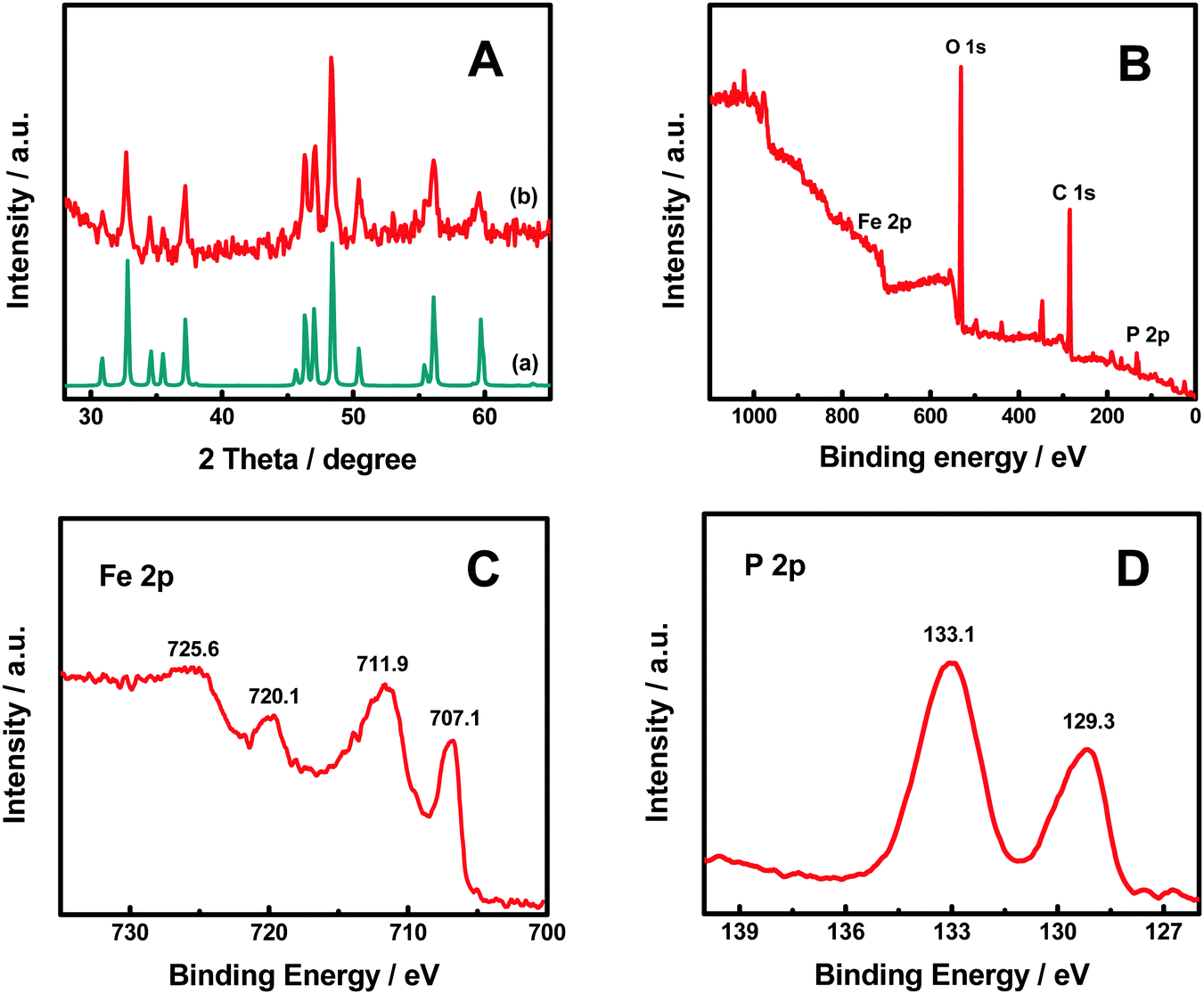 | ||
| Fig. 1 (A) XRD patterns of (a) the FeP nanoparticles and (b) the FeP standard (JCPDF No. 65-2595), (B) XPS survey, (C) Fe 2p core-level, and (D) P 2p core-level XPS spectra of the FeP nanoparticles. | ||
The X-ray photoelectron spectroscopy (XPS) survey spectrum in Fig. 1B revealed that Fe, P, O and C elements were present in the FeP nanoparticles. The oxygen is potentially related to ferric hydroxides/oxides, or absorbed water on the surface. The two peaks at 707.1 and 720.1 eV in the Fe 2p spectrum in Fig. 1C correlate with the 2p3/2 and 2p1/2 of Fe3+ ions in the FeP;39 the other two peaks at 711.9 and 725.6 eV were likely from the 2p3/2 and 2p1/2 of Fe3+ ions likely in the form of FeO(OH) on the surface of the FeP nanoparticles.39 The peaks at 129.3 and 133.1 eV in the P 2p spectrum in Fig. 1D were from the 2p3/2 and 2p1/2 of P3− ions in the FeP nanoparticles.39
The transmission electron microscopy (TEM) image (Fig. 2A) shows that the FeP nanoparticles were aggregated with a primary particle size of about 50 to 60 nm. As the average crystallite size was about 26.1 nm based on the XRD analysis, each particle had 2–3 crystalline domains. The high-resolution transmission electron microscopy (HRTEM) image (Fig. 2B) displayed clear lattice fringes with a spacing value of 0.290 nm from the (002) crystal plane of the FeP nanoparticles, indicating the high crystallinity of the FeP nanoparticles.
 | ||
| Fig. 2 (A) TEM and (B) HRTEM images of FeP nanoparticles. | ||
Fig. 3A shows the reflection loss (RL) curves of the FeP nanoparticles in the frequency range of 1.0–18.0 GHz. The FeP nanoparticles were embedded in paraffin wax for the measurements. Paraffin wax is transparent in the testing frequency range and does not have much absorption.3 As demonstrated for all samples tested with thickness between 1.0 and 6.0 mm, a large reflection loss peak is observed with minimal values between −30 and −40 dB, and sizable sections of the tested frequency range are below −10 dB. RL of −10 dB means that the reflection loss is 90%, and RL of −30 and −40 dB means that the reflection loss is 99.9 and 99.99 percent, respectively. In other words, RL of −10 dB indicates that absorption is 90%, and RL of −30 and −40 dB means absorption is 99.9 and 99.99%. As such Fig. 3A indicates that the FeP nanoparticles demonstrate a very impressive overall microwave absorption performance. The 2D contour plot of RL vs. f & d in Fig. 3B clearly demonstrates the evolution of the microwave absorption as the frequency and thickness vary.
 | ||
| Fig. 3 (A) The RL curves of the FeP nanoparticle absorbers in the frequency (f) range of 1.0–18.0 GHz, (B) the 2D contour plot of RL vs. f & d, (C) the relationships of the microwave absorbing peak frequency (fmax/GHz), (D) the maximum absorbing peak value (RLmax/dB) and (E) the critical absorbing peak width (Δf10/GHz) with the thickness (d/mm) of the FeP nanoparticle absorbers. The dashed green lines in (B)–(D) are the visual guidelines. | ||
To better understand the microwave absorption performance of FeP nanoparticles, Fig. 3C displays the relationship between the microwave absorbing peak frequency (fmax/GHz) and the thickness (d/mm) of the FeP nanoparticle absorbers. Clearly, as the thickness increases, the peak frequency shifts to lower values. Specifically, as the thickness of the absorber increased from 1.0 to 6.0 mm, the peak frequency decreased almost linearly from 15.1 to 8.86 GHz, as can be seen from the straight dashed green line shown in the graph.
The relationships between the maximum absorbing peak value (RLmax/dB) and the thickness (d/mm) are shown in Fig. 3D. Apparently, all the FeP absorbers under test with thickness between 1.0 and 6.0 mm have a RLmax value between −30 and −40 dB, or a maximal absorption efficiency between 99.9 and 99.99 percent. This indicates that as long as those FeP nanoparticles are prepared with a thickness within such a range, good microwave absorption efficiency would be readily achieved. This characteristic gives us large flexibility and feasibility in coating a target surface without worrying so much on the fine controls of the thickness to meet an absorbing capability requirement, because more commonly, a small change in the thickness of the absorbing material will largely affect the efficiency of the absorption.3–24
Fig. 3E displays the relationship between the critical absorbing peak width (Δf10/GHz) and the thickness (d/mm) of the FeP nanoparticle absorbers. Here, the RL of −10 dB is used as a critical value, as it indicates that 90% of the incident microwave electromagnetic field is effectively neutralized with respect to detection. Therefore, the frequency range with a RL value of −10 dB or more is expressed as the critical absorbing peak width (Δf10/GHz). The larger the Δf10 width, the more useful the coating is, as it can shield microwave radiation in a broader frequency range.
As shown in Fig. 3E, when the thickness of the absorber becomes bigger, the critical absorbing peak width (Δf10/GHz) increases in a pseudo-linear fashion. Specifically, Δf10 was enhanced from about 2.90 to 9.60 GHz as the thickness increased from 1.0 to 6.0 mm. This indicates that the thickness of the FeP microwave absorber could be used to effectively expand the effective shielding frequency range.
To further understand the microwave absorption performance of the FeP nanoparticles, their dielectric and magnetic properties are analyzed, as they are related to the reflection loss (RL) value through the following equations:
| RL (dB) = 20 log |(Zin − Z0)/(Zin + Z0)| | (1) |
| Zin = Z0(μr/εr)1/2tanh [j(2πfd/c)(μrεr)1/2] | (2) |
Fig. 4A shows the complex permittivity (ε′, ε′′, tg![[thin space (1/6-em)]](https://www.rsc.org/images/entities/char_2009.gif) δε) of the FeP nanoparticles in the frequency range of 1.0–18.0 GHz. The ε′ value starts with 17.7 at 1.0 GHz, gradually increases to 18.7 at 14.1 GHz and then decreases to 14.0 at 18.0 GHz; the ε′′ value climbs slowly from 0.62 at 1.0 GHz to 1.76 at 12.0 GHz and then quickly shoots up to 11.5 at 18.0 GHz; tgδε gradually changes from 0.03 at 1.0 GHz to 0.10 at 12.0 GHz and then quickly soars to 0.81 at 18.0 GHz, with a similar trend as ε′′. ε′, ε′′ and tgδε = ε′′/ε′ reflect the stored, lost electrical energy and the power loss ratio within the medium. The above results suggest that the FeP nanoparticles have an increasing stored electrical energy as the frequency of the incident electromagnetic field increased. This seems to indicate that, as the frequency of the incident field is increased, the echoes of the electric field, or dipoles in the FeP nanoparticles to the oscillating field, were catching up more rapidly. The intensification of ε′′ and tgδε as a function of frequency suggests that the consumed electrical energy also increased with respect to the said frequency.
δε) of the FeP nanoparticles in the frequency range of 1.0–18.0 GHz. The ε′ value starts with 17.7 at 1.0 GHz, gradually increases to 18.7 at 14.1 GHz and then decreases to 14.0 at 18.0 GHz; the ε′′ value climbs slowly from 0.62 at 1.0 GHz to 1.76 at 12.0 GHz and then quickly shoots up to 11.5 at 18.0 GHz; tgδε gradually changes from 0.03 at 1.0 GHz to 0.10 at 12.0 GHz and then quickly soars to 0.81 at 18.0 GHz, with a similar trend as ε′′. ε′, ε′′ and tgδε = ε′′/ε′ reflect the stored, lost electrical energy and the power loss ratio within the medium. The above results suggest that the FeP nanoparticles have an increasing stored electrical energy as the frequency of the incident electromagnetic field increased. This seems to indicate that, as the frequency of the incident field is increased, the echoes of the electric field, or dipoles in the FeP nanoparticles to the oscillating field, were catching up more rapidly. The intensification of ε′′ and tgδε as a function of frequency suggests that the consumed electrical energy also increased with respect to the said frequency.
 | ||
| Fig. 4 (A) The complex permittivity (ε′, ε′′, tgδε) and (B) complex permeability (μ′, μ′′, tgδμ) of FeP nanoparticles in the frequency range of 1.0–18.0 GHz. | ||
The permeability parameters (μ′, μ′′, and tgδμ) of the FeP nanoparticles are shown in Fig. 4B. The μ′ increases from 0.99 at 1.0 GHz to 1.03 at 4.5 GHz, then decreases to 0.82 at 16.8 GHz and finally climbs to 0.91 at 18.0 GHz; the μ′′ decreases from 0.09 at 1.0 GHz to 0.02 at 12.0 GHz and then increases to 0.57 at 18.0 GHz; tgδμ starts with 0.09 at 1.0 GHz and gradually decreases to 0.02 at 12.0 GHz, only to then surge to 0.63 at 18.0 GHz. The change of tgδμ with respect to the frequency matches well with that of μ′′ with the frequency. Since μ′, μ′′ and tgδμ (which is μ′′/μ′) reflect the stored magnetic energy, lost magnetic energy, and the power loss ratio within the medium, these results suggest that the stored magnetic energy slightly spirals up with the frequency from 1.0 to 12.0 GHz, but then falls off from 12.0 to 16.8 GHz, only to subsequently reclimb from 16.8 to 18.0 GHz, while the lost magnetic energy and the magnetic power loss ratio drop slightly from 1.0 to 12.0 GHz, but then increase from 12.0 to 18.0 GHz. From Fig. 4A and B, we can see that both ε′′ (and tgδε) and μ′′ (and tgδμ) grew slowly from 1.0 to 12.0 GHz, but shot up rapidly from 12.0 to 18.0 GHz.
In order to understand the microwave absorption performance of the FeP nanoparticles, we have further examined their electrical conductivity (σ) and the skin-depth (δ) of microwave radiation in the FeP nanoparticles. The σ curve in the frequency range of 1–18 GHz is shown in Fig. 5A. The σ is calculated with σ (S m−1) = 2πfε0ε′′, where ε0 is the free space permittivity (8.854 × 10⁻¹² F m−1), f is the frequency (Hz), and ε′′ is the imaginary component of permittivity.1,42σ increases gradually from 0.03 to 1.08 S m−1 as the frequency changes from 1.0 to 12.0 GHz and then to 11.56 S m−1 at 18.0 GHz. The σ values indicate that the FeP nanoparticles have good electrical conductivity in the microwave frequency range, or in other words, there is an efficient electrical relaxation channel for the incoming microwave radiation in the FeP nanoparticles, which allows the decay of the microwave radiation as it enters the FeP nanoparticles. This is verified with the δ curve of the microwave radiation as shown in Fig. 5B. The δ value is calculated with (δ/m) = (πfμ0μrσ)−1/2, where μ0 is the permeability of free space (4π × 10−7 H m−1), μr is the relative permeability, and σ is the electrical conductivity (S m−1).1,42δ decreases monotonically from 78.18 to 4.56 mm as the frequency increases from 1.0 to 18.0 GHz. The δ value indicates how deep the microwave radiation needs to go inside the materials to get its intensity decayed to 1/e times. The small δ values in larger frequency ranges indicates that the microwave radiation with higher frequency decays faster inside the FeP nanoparticles, consistent with the large RL values in the higher frequency range.
 | ||
| Fig. 5 (A) σ and (B) δ curve of the FeP nanoparticles in the frequency range of 1.0–18.0 GHz. (C) A schematic illustration of the microwave absorption of FeP nanoparticles. | ||
On the other hand, as shown in eqn (1), the RL is largely controlled by Zin – the input impedance of the absorber which itself depends on (μr/εr)1/2, (μrεr)1/2 and d – the thickness of the absorber (eqn (2)). Our studies show that RL is determined by the coplay of those three major variables. A good match of μr, εr and d is commonly believed to ultimately determine the efficiency of a given microwave absorber.3–24 As seen from Fig. 4A and B, μr and εr in the frequency range change in the opposite directions as the frequency changed, but in the high frequency range, they change in the same direction. This suggests that (μrεr)1/2 has a small variation in the lower frequency range but a large value in the higher frequency range, while (μr/εr)1/2 has an opposite trend. Since the effective microwave absorption mainly occurs in the high frequency range, this observation indicates that the product of μr and εr (μrεr) might play a big role in the microwave absorption of FeP nanoparticles. Meanwhile, as the thickness of the FeP absorber is increased from 1.0 to 6.0 mm, the overall RL is maintained as constant. This indicates that the thickness may not play a big role in the efficiency of the absorption, so long as the thickness is larger than some critical value. Fig. 5C displays the schematic illustration of the microwave absorption mechanism of the FeP nanoparticles. As the microwave radiation encounters the FeP nanoparticles, it echoes with polar rotations and likely with some magnetic domain resonance. The existence of the polar rotations can be seen from the large tgδε and σ values which indicate the efficient electrical relaxation of the microwave radiation inside the FeP nanoparticles. Similarly, the existence of the magnetic domain resonance can be foreseeable based on the large tgδμ values, especially at higher frequencies. The sources of the polar rotations can be traced back to the apparently polar Fe–P bonds, the asymmetrical lattice structure of the FeP nanoparticles, and the apparent asymmetrical structure on the surface and in the interfaces between adjacent nanoparticles, causing internal and interfacial polarization. The sources of the magnetic resonance can be understood in that there are unpaired electrons in the Fe3+ 3d orbitals which can apparently induce spin states to echo with the incoming electromagnetic field of the microwave radiation. The efficient decay of the microwave radiation can be seen from the small δ value and the large RL curves. As shown in Fig. 3B and D, a thicker absorber can shift the absorbing frequency to a lower frequency, as well as widen the absorbing ranges, therefore making the FeP nanoparticles a promising and tunable microwave absorbing material.
Conclusions
In summary, we have shown for the first time that FeP nanoparticles prepared through a thermal phosphorization process display large microwave reflection losses and high absorption performance. A large reflection loss of −37.68 dB at 13.6 GHz has been obtained with a large absorption efficiency of over 99.9%. Furthermore, the thickness of the FeP nanoparticle microwave absorber can be used to tune both the microwave absorbing peak frequency (fmax) between 15.1 and 8.86 GHz and the critical absorbing peak width (Δf10: peak width at RL = −10 dB), while keeping a large reflection loss below −30.0 dB to maintain a high absorption performance. These characteristics thus show that FeP nanoparticles can act as a new and promising microwave absorbing material.Experimental
The FeP nanoparticles were obtained through a thermal phosphorization process following our previous work.31 Briefly, suitable amounts of α-Fe2O3 and NaH2PO2·H2O were ground and heated in argon at 350 °C for 3 h, followed by a thorough wash in HCl and a drying process at 100 °C. The crystal structure of the formed FeP nanoparticles was examined on a Rigaku Miniflex X-ray Diffractometer (XRD) with a Cu Kα (λ = 0.15418 nm) radiation source. The morphologies and crystallinity of the FeP nanoparticles were studied with transmission electron microscopy (TEM) and high resolution transmission electron microscopy (HRTEM). XPS data were collected using a Kratos Axis 165 X-ray photoelectron spectrometer with an Al/Mg dual-anode X-ray source, using a photon beam of 1486.6 eV. All the spectra were calibrated to the carbon peak at 284.6 eV from the carbon tape used to fix the sample. The complex permittivity and permeability of the FeP nanoparticles were measured in the frequency range of 1.0–18.0 GHz using a HP8722ES network analyzer at room temperature with ring-shaped samples containing 60 wt%. Nanoparticles dispersed in paraffin wax, which was cast into a ring mold with a thickness of 1.0–6.0 mm, an inner diameter of 3 mm, and an outer diameter of 7 mm. 60 wt% was chosen as the concentration in order to maintain consistency with other samples in our previous studies.28–32 The size of the ring was carefully controlled by polishing after the ring was pressed. Parrafin wax is transparent to microwave radiation and is commonly used as the dispersing matrix for microwave absorption measurements.Conflicts of interest
The authors herein declare no conflicts of interest.Acknowledgements
X. C. appreciates the support from the U. S. National Science Foundation (DMR-1609061), and the College of Arts and Sciences, University of Missouri-Kansas City. L. T. thanks the National Natural Science Foundation of China (No. 51302072) and China Scholarship Council for their financial support. X. Tan thanks the support from the National Natural Science Foundation of China (11374181).Notes and references
- D. Micheli, Radar absorbing materials and microwave shielding structures design: By using multilayer composite materials, nanomaterials and evolutionary computation, LAP LAMBERT Academic Publishing, 2011 Search PubMed.
- Y. Duan and H. Guan, Microwave absorbing materials, Pan Stanford, Singapore, 2016 Search PubMed.
- D.-L. Zhao, X. Li and Z.-M. Shen, Compos. Sci. Technol., 2008, 68, 2902 CrossRef CAS.
- L. Deng and M. Han, Appl. Phys. Lett., 2007, 91, 023119 CrossRef.
- Z. Fan, G. Luo, Z. Zhang, L. Zhou and F. Wei, Mater. Sci. Eng., B, 2006, 132, 85 CrossRef CAS.
- T. H. Ting, Y. N. Jau and R. P. Yu, Appl. Surf. Sci., 2012, 258, 3184 CrossRef CAS.
- Z. Liu, G. Bai, Y. Huang, F. Li, Y. Ma, T. Guo, X. He, X. Lin, H. Gao and Y. Chen, J. Phys. Chem. C, 2007, 111, 13696 CAS.
- M. H. Al-Saleh and U. Sundararaj, Carbon, 2009, 47, 1738 CrossRef CAS.
- M. H. Al-Saleh, W. H. Saadeh and U. Sundararaj, Carbon, 2013, 60, 146–156 CrossRef CAS.
- X. Ji, M. Lu, F. Ye and Q. Zhou, Adv. Mech. Eng. Appl., 2012, 3, 294 Search PubMed.
- T. Zou, N. Zhao, C. Shi and J. Li, Bull. Mater. Sci., 2011, 34, 75 CrossRef CAS.
- Y. Zhang, Y. Huang, T. Zhang, H. Chang, P. Xiao, H. Chen, Z. Huang and Y. Chen, Adv. Mater., 2015, 27, 2049 CrossRef CAS PubMed.
- X. Bai, Y. Zhai and Y. Zhang, J. Phys. Chem. C, 2011, 115, 11673 CAS.
- L. Olmedo, P. Hourquehie and F. Jousse, Adv. Mater., 1993, 5, 373 CrossRef CAS.
- P. Chandrasekhar and K. Naishadham, Synth. Met., 1999, 105, 115 CrossRef CAS.
- Z. H. Wang, Z. Han, D. Y. Geng and Z. D. Zhang, Chem. Phys. Lett., 2010, 489, 187 CrossRef CAS.
- O. Chiscan, I. Dumitru, P. Postolache, V. Tura and A. Stancu, Mater. Lett., 2012, 68, 251 CrossRef CAS.
- A. Yan, Y. Liu, Y. Liu, X. Li, Z. Lei and P. Liu, Mater. Lett., 2012, 68, 402 CrossRef CAS.
- B. Lan, M. Sun, T. Lin, G. Cheng, L. Yu, S. Peng and J. Xu, Mater. Lett., 2014, 121, 234 CrossRef CAS.
- C. C. Yang, Y. J. Gung, W. C. Hung, T. H. Ting and K. H. Wu, Compos. Sci. Technol., 2010, 70, 466 CrossRef CAS.
- C.-H. Peng, H.-W. Wang, S.-W. Kan, M.-Z. Shen, Y.-M. Wei and S.-Y. Chen, J. Magn. Magn. Mater., 2004, 284, 113 CrossRef CAS.
- C. Sun, K. Sun and P. Chui, J. Magn. Magn. Mater., 2012, 324, 802 CrossRef CAS.
- A. N. Yusoffa and M. H. Abdullah, J. Magn. Magn. Mater., 2004, 269, 271 CrossRef.
- H.-M. Xiao, X.-M. Liu and S.-Y. Fu, Compos. Sci. Technol., 2006, 66, 2003 CrossRef CAS.
- R. C. Che, L.-M. Peng, X. F. Duan, Q. Chen and X. L. Liang, Adv. Mater., 2004, 16, 401 CrossRef CAS.
- X. Qi, J. Xu, Q. Hu, W. Zhong and Y. Du, Mater. Sci. Eng., B, 2015, 198, 108 CrossRef CAS.
- X. Qi, Y. Yang, W. Zhong, Y. Deng, C. Au and Y. Du, J. Solid State Chem., 2009, 182, 2691 CrossRef CAS.
- T. Xia, C. Zhang, N. A. Oyler and X. Chen, Adv. Mater., 2013, 25, 6905 CrossRef CAS PubMed.
- T. Xia, C. Zhang, N. A. Oyler and X. Chen, J. Mater. Res., 2014, 29, 2198 CrossRef CAS.
- L. Tian, J. Xu, M. Just, M. Green, L. Liu and X. Chen, J. Mater. Chem. C, 2017, 5, 4645 RSC.
- T. Xia, Y. Cao, N. A. Oyler, J. Murowchick, L. Liu and X. Chen, ACS Appl. Mater. Interfaces, 2015, 7, 10407 CAS.
- L. Tian, X. Yan, J. Xu, P. Wallenmeyer, J. B. Murowchick, L. Liu and X. Chen, J. Mater. Chem. A, 2015, 3, 12550 CAS.
- J. Dong, R. Ullal, J. Han, S. Wei, X. Ouyang, J. Dong and W. Gao, J. Mater. Chem. A, 2015, 3, 5285 CAS.
- Y. Chen, D. Yang, Y. J. Yoon, X. Pang, Z. Wang, J. Jung, Y. He, Y. W. Harn, M. He, S. Zhang, G. Zhang and Z. Lin, J. Am. Chem. Soc., 2017, 139, 12956 CrossRef CAS PubMed.
- Y. Chen, Y. Yoon, X. Pang, Y. He, J. Jung, C. Feng, G. Zhang and Z. Lin, Small, 2016, 12, 6714 CrossRef CAS PubMed.
- C. Feng, X. Pang, Y. He, Y. Chen, G. Zhang and Z. Lin, Polym. Chem., 2015, 6, 5190 RSC.
- X. Liu, J. Ioccozia, Y. Wang, X. Cui, Y. Chen, S. Zhao, Z. Li and Z. Lin, Energy Environ. Sci., 2017, 10, 402 CAS.
- X. Li, J. Iocozzia, Y. Chen, S. Zhao, X. Cui, W. Wang, H. Yu, S. Lin and Z. Lin, Angew. Chem., Int. Ed., 2018, 57, 2046 CrossRef CAS PubMed.
- L. Tian, X. Yan and X. Chen, ACS Catal., 2016, 6, 5441 CrossRef CAS.
- Y. Xu, R. Wu, J. Zhang, Y. Shi and B. Zhang, Chem. Commun., 2013, 49, 6656 RSC.
- J. F. Callejas, J. M. McEnaney, C. G. Read, J. C. Crompton, A. J. Biacchi, E. J. Popczun, T. R. Gordon, N. S. Lewis and R. E. Schaak, ACS Nano, 2014, 8, 11101 CrossRef CAS PubMed.
- M. Green, L. Tian, P. Xiang, J. Murowchick, X. Tan and X. Chen, Mater. Today Nano Search PubMed , accepted.
| This journal is © the Partner Organisations 2018 |