Universality of the giant Seebeck effect in organic small molecules†
Hirotaka
Kojima
 *a,
Ryo
Abe
a,
Fumiya
Fujiwara
a,
Mario
Nakagawa
a,
Kohtaro
Takahashi
a,
Daiki
Kuzuhara
 b,
Hiroko
Yamada
 a,
Yumi
Yakiyama
 c,
Hidehiro
Sakurai
 c,
Tatsuya
Yamamoto
d,
Hidenori
Yakushiji
d,
Masaaki
Ikeda
d and
Masakazu
Nakamura
 *ae
*ae
aGraduate School of Materials Science, Nara Institute of Science and Technology, Ikoma, Nara 630-0192, Japan. E-mail: kojimah@ms.naist.jp; mnakamura@ms.naist.jp; Fax: +81-743-72-6047; Tel: +81-743-72-6031
bDepartment of Materials Science and Engineering, Faculty of Science and Engineering, Iwate University, Morioka, Iwate 020-8551, Japan
cDivision of Applied Chemistry, Graduate School of Engineering, Osaka University, Suita, Osaka 565-0871, Japan
dCenter for Innovative Research, Nippon Kayaku Co., Ltd, Tokyo 115-8588, Japan
eResearch Center of Integrative Molecular Systems, Institute for Molecular Science, Okazaki, Aichi 444-8787, Japan
First published on 22nd February 2018
Abstract
To explore the universality of the giant Seebeck coefficient (>100 mV K−1) found in our previous study with pure C60 thin films, the thermoelectric properties of high-mobility small-molecule organic semiconductors and their temperature dependencies are investigated. Consequently, various pure organic semiconductors exhibited similar large Seebeck coefficients within the temperature range of 300–360 K. The magnitude of the Seebeck coefficient, its intense temperature dependence, and correlation with the activation energy of electrical conductivity are unique and cannot be elucidated by currently known physical models of thermoelectricity.
Recent years have seen the development of thermoelectric (TE) materials as a means for harvesting electricity from heat typically wasted in daily life. To harvest this widespread waste heat, fabrication of flexible and large-area devices at low cost is required. Organic-based materials are advantageous owing not only to their compatibility with printed flexible devices but also to their low thermal conductivity. Although polymeric semiconductors/conductors1–6 and some charge-transfer complexes7–12 are relatively well investigated, small-molecule semiconductors have not been studied enough because of the difficulty in obtaining high conductivity crystals or thin films without chemical doping, which is necessary to satisfy the conventional criteria; the power factor is maximized when a semiconductor is heavily doped.13–16
The performance of TE materials is in general determined by the dimensionless figure of merit, ZT = α2σT/κ (α: Seebeck coefficient, σ: electrical conductivity, κ: thermal conductivity, and T: absolute temperature), or the power factor, PF = α2σ. A small κ in organic materials is therefore an advantage to obtain high ZT.17 In terms of σ, organic materials are not superior to inorganic materials because of their low carrier mobility and the ineffective carrier doping. However, the loss of ZT through a low σ can possibly be compensated for by finding novel phenomena or materials to obtain a high α, because ZT is proportional to the square of α. In organic solids, not only the carrier but also the phonon, or molecular vibration, tends to localize within a molecule, which increases the chance of the interaction between them. It is therefore natural to expect unknown thermoelectric phenomena to be found in organic materials. In spite of this, the thermoelectricity of organic solids has not been well studied even from the scientific point of view, while inorganic solids have been studied for more than a hundred years.
In our previous work, we have reported a giant Seebeck effect (GSE) in pure C60 thin films, where α reaches over 150 mV K−1.18 C60 is not strictly an organic material but its packing structure and electronic nature are similar to organic small molecules. The GSE must therefore also appear in organic molecular solids. Herein, the TE properties, such as Seebeck coefficient and electrical conductivity, are broadly surveyed for various small-molecule organic semiconductors with relatively high carrier mobilities. Several representative organic semiconductors are selected in which the conduction type in a crystalline state distributes from one- to three-dimensional, and long alkyl chains are introduced into some of the skeletons, to test the influence of the expansion and the structural modulation by temperature on the GSE (Fig. 1). Here, the dimensionality of the conduction was tuned by changing the proportion of molecules from rod-like to disk-like because a wider molecular plane tends to induce a stronger π-stacking nature.19–21 The requirements and characteristics of the GSE are shown and discussed for the future study on the physical and chemical origins of this unique phenomenon.
Purified organic semiconducting materials were used in the experiments. Details of the materials used in this work are described in the Experimental procedure section. All of the thin-film samples were prepared by vacuum deposition using a Knudsen cell in a measurement chamber (Fig. 2a), which was evacuated down to ultra-high vacuum (<10−7 Pa). The thin film was deposited onto a glass substrate with a pair of pre-wired gold/chromium electrodes with 30/3 nm thicknesses, respectively. Each electrode was separated so as to form an “i”-shape, which is necessary to avoid the interference between the temperature and thermoelectromotive force measurements for highly resistive samples (Fig. 2b). The temperature difference was measured by two K-type (alumel/chromel) thermocouples fixed on the small dots of the “i”-shaped electrodes. The thermoelectromotive force (output voltage, ΔV) was measured between the long bars of the “i”-shaped electrodes through copper wires. The gap of the electrodes (L) was 5 mm, which is long enough to ignore the influence of the contact on the conductance and Seebeck measurements. During the Seebeck measurements, a uniform and one-dimensional temperature gradient was applied to the top plate of the sample folder using a small heater and the “i”-shaped electrodes were aligned perpendicular to the temperature gradient to guarantee the accuracy of the temperature difference (ΔT) between two contacting electrodes. The conductance and Seebeck coefficient of the sample were measured in situ using a source measurement unit (Keithley 6430) and a lab-made differential amplifier22 connected to a digital multimeter (Keithley 2000), respectively. Either of two measurement systems was connected to the contacting electrodes from outside of the chamber depending on the type of measurement. Owing to the electrode design and the high-input-impedance differential amplifier, this system can measure the Seebeck coefficient of a resistive sample even up to 1014 Ω. Thicknesses of the films were measured using a stylus profilometer after the in situ electrical and thermoelectric measurements to calculate electrical conductivities.
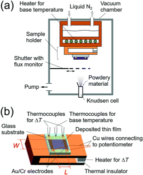 | ||
| Fig. 2 Schematic illustrations of (a) the measurement chamber and (b) the sample holder used in this work. | ||
Fig. 3 shows a typical time profile of the ΔV and ΔT. ΔV is almost correctly proportional to ΔT, except the transient behaviour until the temperature distribution of the sample folder reaches an equilibrium state. ΔV is tolerably stable over 10 min at each ΔT step. This indicates that the GSE is a steady-state phenomenon against the application of the temperature difference. The Seebeck coefficient is defined as α = −ΔV/ΔT and the sign of α calculated as shown in Fig. 3 is negative, indicating that the dominant carrier of this sample, C8BTBT, is the electron.
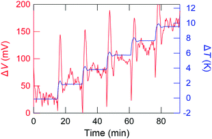 | ||
| Fig. 3 A typical time profile of temperature difference (ΔT) and thermoelectromotive force (ΔV) during the Seebeck measurement for C8BTBT. | ||
α and σ of the materials tested in this work are summarized in Fig. 4. The connected circles from left to right correspond to the values at lower to higher temperatures for all of the samples where σ increased monotonically with temperature (see also Fig. S1, ESI†). Most of the compounds tend to give negative Seebeck coefficients (filled circles) even though some of them are known as p-channel materials in field-effect transistors (FETs). The difference in the polarity is not surprising because the channel type in an FET is mainly determined by the injection barrier from the electrodes, but the sign of the Seebeck coefficient reflects the contribution to the bulk conductivity.
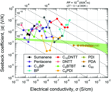 | ||
| Fig. 4 Seebeck coefficient (α) and electrical conductivity (σ) of small-molecule organic semiconductors and their temperature dependence. Filled and open circles denote negative and positive Seebeck coefficients, respectively. The connected circles from left to right correspond to from a lower to higher temperature for all of the samples. The range and step of the measurement temperature for each compound are described in the Experimental section. The green region shows predicted values by the conventional thermoelectric theory for non-degenerate semiconductors calculated with γ = −0.5, m*/m0 = 1, and μ = 0.01–1 cm2 V−1 s−1.18 | ||
A green-highlighted area in Fig. 4 indicates the predicted range of α(σ) by the conventional theory for non-degenerate semiconductors, which is expressed by:
 | (1) |
According to the conventional theory, eqn (1) can be also expressed as:
 | (2) |
| Compound | HOMO (eV) | LUMO (eV) | E g (eV) | λ e (meV) | λ h (meV) |
|---|---|---|---|---|---|
| Pentacene | −4.61 | −2.40 | 2.21 | 132 | 94 |
| DNTT | −5.19 | −1.82 | 3.37 | 205 | 132 |
| PDI | −6.11 | −3.58 | 2.53 | 246 | 152 |
| PDA | −6.47 | −3.92 | 2.55 | 252 | 146 |
| BP | −4.70 | −2.28 | 2.42 | 158 | 54 |
In some inorganic materials, the so-called phonon drag enhances α at low temperature.25 The contribution of the phonon drag is known to become maximum at around TD/4,26 where TD is the Debye temperature. However, even if it appears also in the organic solids used in this work, its contribution must be negligible in the temperature range, 300–400 K, because the TD of typical organic semiconductors is lower than 300 K, e.g. 125–216 K for pentacene27,28 and 63 K for rubrene.29 Therefore, the GSE must have arisen from a different principle from that for such inorganic materials.
Here, we would like to consider the reason why the GSE was not observed in perylene derivatives. Among the two-dimensional grazing-incidence X-ray diffraction (2D-GIXD) patterns obtained from the thin films used in this work (Fig. S3, ESI†), the tendency to align the molecular planes parallel to the substrate (often referred to as “face-on” orientation) was the strongest in perylene derivatives. The parallel orientation means that the Seebeck coefficient was measured along a lower mobility direction. The Seebeck measurements along the high-mobility direction are therefore assumed to be important to exhibit the GSE.
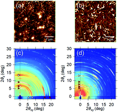
To confirm this assumption, a differently oriented BP film was tested using a flattened sapphire substrate, because some planar molecules are known to change their orientations by controlling the atomic-scale flatness of the substrate.30 The atomic step-terrace structure is formed on the sapphire surface by annealing the substrate at 1000 °C for 10 hours in an oxygen atmosphere (Fig. S4, ESI†). When BP was deposited onto this substrate, smooth grains were observed in wide areas, in which the molecules are in parallel orientation, while sharp needle-like grains, in which they are in the near-perpendicular orientation, were dominant on the glass substrate (Fig. 5a and b). As a result, the ratio of parallel-orientation grains on the flattened-sapphire substrate (69%) is larger than that on the glass substrate (46%), which is also in good agreement with the difference in the GIXD patterns (Fig. 5c and d). The temperature dependence of the Seebeck coefficients for the differently oriented BP films is shown in Fig. 6. On the flattened-sapphire substrate, the Seebeck coefficient is suppressed to an ordinary value, 1–10 mV K−1, in a lower temperature range under 360 K, which is in contrast to the large Seebeck coefficient on the glass substrate. However, in a higher temperature range, the GSE, of which the peak value is relatively low, appears even for the film on the flattened-sapphire substrate. These results suggest that the increase in the parallel-orientation grains decreases the chance of the connections of the perpendicular-orientation grains along the current path and thereby suppress the appearance of the GSE. Some of other molecules, e.g. C12BP and C10DNTT, also form thin films with mixed orientations (Fig. S3(b) and (f), ESI†) but exhibited a large Seebeck coefficient. This can be also explained by the ratio of the parallel-orientation grains in these films, which is similar to that of the BP on the glass substrate.
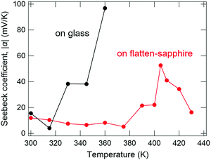 | ||
| Fig. 6 Temperature dependence of the Seebeck coefficient of BP thin films on glass and flatten sapphire substrates. | ||
Next, we would like to discuss the meaning of an empirically determined condition necessary for the observation of the GSE: low conductivity. As a general tendency, the GSE commonly exhibits low conductivity, as shown in Fig. 3 (σ < 10−5 S cm−1), which corresponds to a carrier concentration of ca. 6 × 1014 cm−3 if a typical mobility of the thin films of these materials was assumed to be 0.1 cm2 V−1 s−1. Under such a low carrier concentration, more localized states, or shallow traps, govern the conductivity and the carrier transport become hopping-like.31 On the other hand, when the carrier concentration becomes high, e.g. >1019 cm−3 as in the channel region of FETs, more delocalized states are also occupied by the carriers and the carrier transport becomes band-like. Accordingly, the two different mechanisms of carrier transport coexist in the intermediate concentration range. The Seebeck coefficient in such a case can be expressed by the two-band model:
 | (3) |
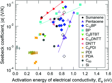
When the hopping-like transport is dominant, the electrical conductivity frequently becomes a thermally activated type with an approximated formula: σ = σ0![[thin space (1/6-em)]](https://www.rsc.org/images/entities/char_2009.gif) exp(−Ea/kBT). We therefore calculated the material and temperature dependences of the activation energy of electrical conductivity (Ea) by calculating ∂
exp(−Ea/kBT). We therefore calculated the material and temperature dependences of the activation energy of electrical conductivity (Ea) by calculating ∂![[thin space (1/6-em)]](https://www.rsc.org/images/entities/char_2009.gif) ln
ln![[thin space (1/6-em)]](https://www.rsc.org/images/entities/char_2009.gif) σ/∂(1/T) and found the similarity in the temperature dependences of α and Ea (Fig. S2, ESI†). Fig. 7 summarizes the relationship between α and Ea for all of the samples measured in this work. For comparison, α and Ea values of the n-type silicon crystal measured at different temperatures are also plotted. In the case of normal Seebeck materials including silicon, α is always around 1 mV K−1 and is independent of Ea. However, in the case of giant Seebeck materials, there is a trend where log
σ/∂(1/T) and found the similarity in the temperature dependences of α and Ea (Fig. S2, ESI†). Fig. 7 summarizes the relationship between α and Ea for all of the samples measured in this work. For comparison, α and Ea values of the n-type silicon crystal measured at different temperatures are also plotted. In the case of normal Seebeck materials including silicon, α is always around 1 mV K−1 and is independent of Ea. However, in the case of giant Seebeck materials, there is a trend where log![[thin space (1/6-em)]](https://www.rsc.org/images/entities/char_2009.gif) α becomes proportional to Ea. The meaning of proportionality is still an open question at this stage. However, the large Ea and its significant variation by temperature could be a key issue to understanding the transport phenomena in the giant Seebeck materials.
α becomes proportional to Ea. The meaning of proportionality is still an open question at this stage. However, the large Ea and its significant variation by temperature could be a key issue to understanding the transport phenomena in the giant Seebeck materials.
Electrical conductivity is in general expressed by
| σ = enμ, | (4) |
 | (5) |
 | (6) |
 | (7) |
Substituting eqn (5)–(7) for (4), the strong temperature-dependent factor of the conductivity under high temperature and low electric field can be approximated by
 | (8) |
λ values estimated for isolated molecules by normal modes analysis38 are, however, only 0.1–0.3 meV (Table 1), a quarter of which seems to be too small to contribute to the large variation of Ea by temperature. Therefore, in real materials, we have to consider a more complicated polaron hopping accompanied with lattice distortion. A similar mechanism was investigated in a charge-transfer complex and the Seebeck coefficient tends to be relatively large.39 Excess Ea is therefore considered to arise from not only polarization of the surrounding molecules but also a long-range lattice distortion, which was not accounted for in the above calculations. As mentioned above, the conventional transport equations/calculations that treat electron and phonon transports separately cannot reproduce the extremely large α. We have to consider the assistance of molecular vibrations to understand the extraordinarily large energy per carrier. An essential condition for the GSE is, therefore, considered to be the strong coupling between the carrier and phonon in the system. A novel theoretical approach which combines charge and phonon transport from the Schrödinger equation would be necessary to completely elucidate the GSE.
Finally, it should be noted that the large α, >100 mV K−1, is beneficial also for application in flexible TE generators. Instead of the small α, <0.1 mV K−1, to maintain the maximum PF in conventional TE materials, the GSE gives a chance to use the extremely large α where PF becomes another maximum. This means that the novel TE generators with GSE materials can output >1 V against a temperature difference of 10 K only by a single uni-leg cell. As a result, an innovatively simple structure of the TE generator modules could be realized without fabricating complicated π-type connections of p- and n-type TE materials. Accordingly, the fabrication cost must be decreased and bending tolerance drastically increased. As shown in Fig. 3, the maximum PF obtained in this work is already over 10−4 W K−2 m−1, which corresponds to ZT ≈ 0.005 when we assume a κ value of 0.1 W m−1 K−1 as the typical range for organic solids. Since this subject is still in the initial stage of the study, the value must be improved a lot by understanding the mechanism and optimizing the molecular structure and orientations.
In conclusion, the GSE was universally observed in small-molecule organic semiconductors regardless of the molecular shape. The magnitude of α intensely varied by the temperature and the temperature maximizing α depended on the materials. The major requirements for the GSE are found to be (1) higher mobility to the current direction and (2) low carrier concentration. From many experimental results and deep consideration, we have come to an assumption that the large activation energy of electrical conductivity and its intense temperature dependence closely relate to the key physical process of the GSE. A novel theoretical approach that combines carrier conduction and phonon propagation is necessary to completely elucidate the GSE.
Experimental procedure
Materials
Sumanene, BP, C8BTBT, C10DNTT and DNTT were synthesized according to the literature.40–44 Synthesis of C12BP is described in the ESI.† C60 was purchased from KANTO Chemical Co., Inc. Other materials were purchased from TCI Chemicals. Some materials which had not been sublimation purified when received were further purified by sublimation in a quartz-tube furnace under an argon atmosphere (∼102 Pa) unless otherwise noted in the following sections.Film preparation
Author contributions
M. Nakamura conceived the idea and designed the experiments. R. A., F. F. and M. Nakagawa carried out the experiments. The manuscript has been prepared by H. K. and M. Nakamura. Other authors synthesized the materials. All authors have given approval to the final version of the manuscript.Conflicts of interest
There are no conflicts to declare.Acknowledgements
This work was supported by a Grant-in-Aid for Scientific Research on Innovative Areas “π-System Figuration: Control of Electron and Structural Dynamism for Innovative Functions” from the Japan Society for the Promotion of Science (JSPS) (No. 26102002, 15H01000 and 17H05158), “3D Active-Site Science” from JSPS (No. 26105004) and a Grant-in-aid for Young Scientists (B) (No. 15K21163) (JSPS KAKENHI). The synchrotron radiation experiments were performed at the BL19B2 of SPring-8 with the approval of the Japan Synchrotron Radiation Research Institute (JASRI) (Proposal No. 2015A1843, 2015B1778, 2016B1769, 2016B1903 and 2017B1745). The authors thank Prof. Noriyuki Yoshimoto (Iwate Univ.), Mr Mamoru Kikuchi (Iwate Univ.) and Dr Tomoyuki Koganezawa (JASRI) for GIXD experiments, Ms Yoshiko Nishikawa (NAIST) for mass spectroscopy and Prof. Takeshi Inagaki (Osaka Butsuryo Univ.) for helpful discussions about the mechanism based on polaron conduction. H. K. and M. Nakamura acknowledge the NAIST Green Photonics Research Project (MEXT) for financial support and Prof. Leigh McDowell (NAIST) for linguistic support for the manuscript.Notes and references
- K. Gordiz, A. K. Menon and S. K. Yee, J. Appl. Phys., 2017, 122, 124507 CrossRef.
- N. Lu, L. Li and M. Liu, Phys. Chem. Chem. Phys., 2016, 18, 19503–19525 RSC.
- Q. Zhang, Y. Sun, W. Xu and D. Zhu, Adv. Mater., 2014, 26, 6829–6851 CrossRef CAS PubMed.
- O. Bubnova, Z. U. Khan, A. Malti, S. Braun, M. Fahlman, M. Berggren and X. Crispin, Nat. Mater., 2011, 10, 429–433 CrossRef CAS PubMed.
- G.-H. Kim, L. Shao, K. Zhang and K. P. Pipe, Nat. Mater., 2013, 12, 719–723 CrossRef CAS PubMed.
- M. Culebras, C. Gómez and A. Cantarero, Materials, 2014, 6701–6732 CrossRef PubMed.
- F. Huewe, A. Steeger, K. Kostova, L. Burroughs, I. Bauer, P. Strohriegl, V. Dimitrov, S. Woodward and J. Pflaum, Adv. Mater., 2017, 29, 1605682 CrossRef PubMed.
- Y. Machida, X. Lin, W. Kang, K. Izawa and K. Behnia, Phys. Rev. Lett., 2016, 116, 087003 CrossRef PubMed.
- H. Itahara, M. Maesato, R. Asahi, H. Yamochi and G. Saito, J. Electron. Mater., 2009, 38, 1171–1175 CrossRef CAS.
- T. Mori, H. Inokuchi, A. Kobayashi, R. Kato and H. Kobayashi, Phys. Rev. B: Condens. Matter Mater. Phys., 1988, 38, 5913–5923 CrossRef CAS.
- B. Maennig, M. Pfeiffer, A. Nollau, X. Zhou, K. Leo and P. Simon, Phys. Rev. B: Condens. Matter Mater. Phys., 2001, 64, 195208 CrossRef.
- V. Gama, R. T. Henriques, G. Bonfait, L. C. Pereira, J. C. Waerenborgh, I. C. Santos, M. T. Duarte, J. M. P. Cabral and M. Almeida, Inorg. Chem., 1992, 31, 2598–2604 CrossRef CAS.
- K. Harada, M. Sumino, C. Adachi, S. Tanaka and K. Miyazaki, Appl. Phys. Lett., 2010, 96, 253304 CrossRef.
- K. Hayashi, T. Shinano, Y. Miyazaki and T. Kajitani, J. Appl. Phys., 2011, 109, 23712 CrossRef.
- A. Nollau, M. Pfeiffer, T. Fritz and K. Leo, J. Appl. Phys., 2000, 87, 4340–4343 CrossRef CAS.
- M. Pfeiffer, A. Beyer, T. Fritz and K. Leo, Appl. Phys. Lett., 1998, 73, 3202–3204 CrossRef CAS.
- N. Kim, B. Domercq, S. Yoo, A. Christensen, B. Kippelen and S. Graham, Appl. Phys. Lett., 2005, 87, 241908 CrossRef.
- H. Kojima, R. Abe, M. Ito, Y. Tomatsu, F. Fujiwara, R. Matsubara, N. Yoshimoto and M. Nakamura, Appl. Phys. Express, 2015, 8, 121301 CrossRef.
- B.-T. Wang, M. A. Petrukhina and E. R. Margine, Carbon, 2005, 94, 174 CrossRef.
- H. Kobayashi, N. Kobayashi, S. Hosoi, N. Koshitani, D. Murakami, R. Shirasawa, Y. Kudo, D. Hobara, Y. Tokita and M. Itabashi, J. Chem. Phys., 2013, 139, 014707 CrossRef PubMed.
- M. Hoffmann, Z. G. Soos and K. Leo, Nonlinear Opt., 2002, 29, 227–237 CAS.
- M. Nakamura, A. Hoshi, M. Sakai and K. Kudo, Mater. Res. Soc. Symp. Proc., 2010, 1197 DOI:10.1557/PROC-1197-D09-07.
- K. Seeger, Charge and Energy Transport in a Nondegenerate Electron Gas, Semiconductor Physics: An Introduction, 9th edn, 2004, ch. 4, pp. 47–117 Search PubMed.
- B. Russ, M. J. Robb, F. G. Brunetti, P. L. Miller, E. E. Perry, S. N. Patel, V. Ho, W. B. Chang, J. J. Urban, M. L. Chabinyc, C. J. Hawker and R. A. Segalman, Adv. Mater., 2014, 26, 3473–3477 CrossRef CAS PubMed.
- S. M. Puri, Phys. Rev., 1965, 139, A995–A1009 CrossRef.
- A. B. Kaiser, S. A. Rogers and Y. W. Park, Mol. Cryst. Liq. Cryst., 2004, 415, 115–124 CrossRef CAS.
- M. Fulem, V. Laštovka, M. Straka, K. Růžička and J. M. Shaw, J. Chem. Eng. Data, 2008, 53, 2175–2181 CrossRef CAS.
- R. C. Hatch, D. L. Huber and H. Höchst, Phys. Rev. Lett., 2010, 104, 47601 CrossRef PubMed.
- Y. Okada, M. Uno, Y. Nakazawa, K. Sasai, K. Matsukawa, M. Yoshimura, Y. Kitaoka, Y. Mori and J. Takeya, Phys. Rev. B: Condens. Matter Mater. Phys., 2011, 83, 113305 CrossRef.
- M. Nakamura and H. Tokumoto, Surf. Sci., 1998, 398, 143–153 CrossRef CAS.
- H. Bässler, Phys. Status Solidi B, 1993, 175, 15–56 CrossRef.
- W. C. Germs, K. Guo, R. A. J. Janssen and M. Kemerink, Phys. Rev. Lett., 2012, 109, 16601 CrossRef PubMed.
- K. P. Pernstich, B. Rössner and B. Batlogg, Nat. Mater., 2008, 7, 321–325 CrossRef CAS PubMed.
- S. D. Baranovskii, O. Rubel, F. Jansson and R. Österbacka, Description of Charge Transport in Distorted Organic Materials, Organic Electronics, Advances in Polymer Science, ed. G. Meller and T. Grasser, 2009, pp. 45–71 Search PubMed.
- R. Matsubara, N. Ohashi, M. Sakai, K. Kudo and M. Nakamura, Appl. Phys. Lett., 2008, 92, 242108 CrossRef.
- M. Jakobsson and S. Stafström, J. Chem. Phys., 2011, 135, 134902 CrossRef PubMed.
- G. Verbeek, Chem. Phys. Lett., 1992, 188, 85–92 CrossRef CAS.
- J. R. Reimers, J. Chem. Phys., 2001, 115, 9103–9109 CrossRef CAS.
- M. Dongol, A. El-Denglawey, A. F. Elhady and A. A. Abuelwafa, Appl. Phys. A: Mater. Sci. Process., 2015, 118, 345–351 CrossRef CAS.
- H. Sakurai, T. Daiko and T. Hirao, Science, 2003, 301, 1878 CrossRef CAS PubMed.
- S. Ito, T. Murashima, N. Ono and H. Uno, Chem. Commun., 1998, 1661–1662 RSC.
- H. Ebata, T. Izawa, E. Miyazaki, K. Takimiya, M. Ikeda, H. Kuwabara and T. Yui, J. Am. Chem. Soc., 2007, 129, 15732–15733 CrossRef CAS PubMed.
- M. J. Kang, I. Doi, H. Mori, E. Miyazaki, K. Takimiya, M. Ikeda and H. Kuwabara, Adv. Mater., 2011, 23, 1222–1225 CrossRef CAS PubMed.
- T. Yamamoto and K. Takimiya, J. Am. Chem. Soc., 2007, 129, 2224–2225 CrossRef CAS PubMed.
Footnote |
| † Electronic supplementary information (ESI) available: Detail in the electrical and thermoelectric measurements, 2D-GIXD patterns, AFM images of surface of substrate. See DOI: 10.1039/c7qm00596b |
| This journal is © the Partner Organisations 2018 |


