
PbI2 band gap engineering by gel incorporation†
Chong
Hu
,
Tao
Ye
,
Yujing
Liu
,
Jie
Ren
,
Xinyi
Jin
,
Hongzheng
Chen
 and
Hanying
Li
*
and
Hanying
Li
*
MOE Key Laboratory of Macromolecular Synthesis and Functionalization, State Key Laboratory of Silicon Materials, Department of Polymer Science and Engineering, Zhejiang University, Hangzhou, 310027, China. E-mail: hanying_li@zju.edu.cn
First published on 15th December 2017
Abstract
Incorporation of guest materials into semiconducting single crystalline hosts leads to the formation of semiconducting single-crystal composites. However, limited efforts have been made to comprehensively investigate the property of these potential functionalized single-crystal composites. Herein, PbI2/gel single-crystal composites have been successfully prepared. Diffuse reflectance spectra show a clear increase in the band gap of PbI2 after gel incorporation. The band gap is further increased through expanding the area of host/guest interfaces or enhancing the interatomic forces at the interfaces. The interatomic forces (electrostatic interaction) at the host/guest interfaces are attributed to this band gap shift. As such, this study provides a novel and facile way for band gap engineering by gel incorporation.
 Hanying Li | Hanying Li is the Qiushi Distinguished Professor in the Department of Polymer Science and Engineering at Zhejiang University, China. In Dec. 2009, he completed his PhD degree at Cornell University in the field of materials science and engineering (advisor: Prof. Lara A. Estroff). After postdoctoral work on organic electronics at Stanford University (Prof. Zhenan Bao's group), Hanying Li moved to Zhejiang University in Dec. 2011. His current research focuses on bio-inspired single-crystal growth and organic-single-crystal-based electronic and optoelectronic devices such as transistors and solar cells. |
Introduction
A variety of biominerals, including the skeletal parts of echinoderms and the prismatic layer of mollusk shells, are organic/inorganic (guest/host) single-crystal composites.1–6 Similar to biogenic crystals with incorporated biomacromolecules, increasing examples of synthetic single-crystal hosts have been reported to incorporate foreign material guests including gel-networks.7–12 Gels have been widely used as crystallization media.13 Moreover, gel-networks were found to penetrate the growing crystals; this resulted in crystal/gel-network interpenetrating composite structures.14–21 This kind of single-crystal composites exhibit a long-range order in molecular packing (single-crystallinity) and interpenetrating bulk-contact composite structure, promising for advanced electronic materials.22–25 Interestingly, if guest materials (e.g., nanoparticles) are dispersed in the gel media, subsequent crystallization leads to incorporation of these guests together with the gel-networks; this suggests a facile approach to widely functionalize single crystals with nonintrinsic properties to potentially expand their applications.17,21Aiming at functionalization and application of single-crystal composites, efforts have been made to adopt semiconducting and conducting single crystals, including ZnO,26–30 Cu2O,31,32 PbI2, PbS,19 anthracene, 9,10-diphenylanthracene (DPA),20 and Au,33 as crystalline hosts. However, the effects of the incorporated materials on the electronic properties of the crystal hosts are less frequently studied. Interestingly, Brif et al.27 have found that amino acids can be incorporated into a ZnO crystal host; these incorporated amino acids not only induce lattice strains but also lead to systematic changes in the band gap of the semiconductor host. In addition to the widely used strategies,27,34,35 this study provides an alternative approach to tune the band gap that is a key parameter of semiconducting materials in a multitude of applications.27,35 To make complete use of this novel approach, it is necessary to elucidate the mechanism by which the incorporated foreign materials alter the band gap. Moreover, it remains a question that whether it is a widespread phenomenon that the band gap of a semiconducting crystal host is altered by incorporation of foreign guest materials.
In this study, we examined the band gap value of PbI2 single crystals grown from silica gels. We have demonstrated that the band gap shifts when a silica gel network is incorporated into the PbI2 single crystals. A further shift is realized by either chemically modifying the gel-networks with amino groups or physically introducing silica nanoparticles, and the largest band gap shift is 0.025 eV.
Experimental
Gel preparation and crystal growth
![[thin space (1/6-em)]](https://www.rsc.org/images/entities/char_2009.gif) :1) was added upon each side of the gel to acidize it, which is helpful to prevent production of Pb(OH)I in the subsequent crystallization step.36,37 After 24 hours, CH3COOH on the gel was removed. The process of PbI2 crystallization and separation was the same as described above, except that the solvent used herein was a mixture of ethanol and water with a volume ratio of 3:1.
:1) was added on the gel to acidize it once silica gels were formed and aged for 24 hours. After this, CH3COOH on the gel was removed. Then, 15 mL of 0.1 M KI (ethanol:water = 3:1 volume ratio) was added on the gel to grow the PbI2 crystals. The process of PbI2 separation was the same as described above. Then, 10% v/v gel with CNH2 of 2.5% and 7.5% was made in the same way; the volumes of each precursor are mentioned in Table S1 (ESI†). Herein, CNH2 is defined as the proportion of amino groups in all the side groups (including amino groups and methoxyl groups) of the original siloxanes (TMOS and APTMS).
:1) was added upon each side of the gel to acidize it, which is helpful to prevent production of Pb(OH)I in the subsequent crystallization step.36,37 After 24 hours, CH3COOH on the gel was removed. The process of PbI2 crystallization and separation was the same as described above, except that the solvent used herein was a mixture of ethanol and water with a volume ratio of 3:1.
:1) was added on the gel to acidize it once silica gels were formed and aged for 24 hours. After this, CH3COOH on the gel was removed. Then, 15 mL of 0.1 M KI (ethanol:water = 3:1 volume ratio) was added on the gel to grow the PbI2 crystals. The process of PbI2 separation was the same as described above. Then, 10% v/v gel with CNH2 of 2.5% and 7.5% was made in the same way; the volumes of each precursor are mentioned in Table S1 (ESI†). Herein, CNH2 is defined as the proportion of amino groups in all the side groups (including amino groups and methoxyl groups) of the original siloxanes (TMOS and APTMS).
Dissolution and etching of the crystal
Herein, 4 M Na2S2O3 (SCR, AR) was used to dissolve the PbI2 crystal for optical microscopy (OM) observation. Tetrahydrofuran (THF, SCR, purity ≥99.0%)36 was used to etch the PbI2 crystal for scanning electron microscope (SEM) imaging and energy dispersive X-ray spectroscopy (EDX) mapping.Characterization
The dissolution process of the crystals was imaged using an optical microscope (OM, Nikon LV100 POL) equipped with a digital camera. The average size of the colloidal silica particles was measured by DLS using Malvern Zetasizer Nano-ZS (UK) at 25 °C with a fixed detector angle of 173°. The intensity-average hydrodynamic diameter was used in this study. The morphology and the element contents of the original crystals before and after etching were examined via SEM (HITACHI, S-4800, 20 kV) and EDX (HITACHI, S-4800, 20 kV), respectively. The chemical compositions of the crystals were identified by powder X-ray diffraction (PXRD, RIGAKU D/MAX 2550/PC) after grinding the crystals to powders, and then, PbI2 lattice parameters were deduced by the Rietveld refinement method. For PbI2 crystals, electron-transparent TEM samples were prepared by a dual-beam focused ion beam (FIB) system (FEI Quanta 3D field emission gun with Omni probe). To remove the damaged layer left behind by previous high-kV fast milling procedures, the final surfaces of the sections were finished by a low-dose (2 kV, 8.9 pA) ion-polishing step.18 Then, selected-area electron diffraction (SAED) patterns were obtained using FEI Tecnai F20 (field emission gun, 200 kV). The Si contents of the crystals grown from silica gels were measured using an inductively coupled plasma atomic emission spectrometer (ICP-AES, Thermo, iCAP6300).Band gap measurement
Optical band gap (Eg) value was measured via diffuse reflectance spectroscopy (DRS) using the UV-2450 UV-vis Shimadzu spectrophotometer with a DRA-2500 integrating sphere attachment. The optical reflection was obtained in the 350–700 nm range. After the spectra were obtained, the Eg value was calculated by the Tauc equation: (αhν)1/n = C1(hν − Eg), where h is the Planck's constant, ν is the frequency of vibration, α is the absorption coefficient, Eg is the band gap, C1 is a proportional constant, and n is the corresponding coefficient. For powders, α is not easy to measure; thus, the Kubelka–Munk (KM) model27,38,39 has to be introduced:where R∞ is the relative diffuse reflectance obtained by DRS, K is the effective absorption coefficient, and S is the effective scattering coefficient. In general, K = 2α and S = s. For the powder sample whose size is small (thickness of the sample is much larger than the size of the particles), the scattering coefficient s is constant; thus, F(R∞) is proportional to α. For direct band gap materials such as PbI2, it is well known that n = 1/2.38,40 Thus, the Tauc equation is converted to [F(R∞)hν]2 = C2(hν − Eg). Then, [F(R∞)hν]2 was plotted against hν. There is a linear region on the curve of ([F(R∞)hν]2 − hν). The hν value at the point of intersection of the fitting line and the horizontal axis is the Eg value. The original measured data is provided in Fig. S4 (ESI†); Eg values of each sample and detailed analysis of the error are listed in Table S3 (ESI†).

Results and discussion
PbI2 single crystals have been obtained by the gel method in our previous study, and gel-incorporated composite structure has been proved.19 We first prepared PbI2 grown from different concentrations (5/7.5/10% w/v) of silica gels, where the gels were prepared using the same Si precursor (Na2SiO3·5H2O) as used in a previous study.19 The obtained crystals were confirmed to be PbI2 by PXRD (Fig. S1, ESI†). Subsequently, we examined the internal structure of the PbI2 crystals by monitoring the dissolution of the crystals. When the gel-grown crystal was partially and completely dissolved, translucent residual silica gels were left with almost the same hexagonal shape as the original PbI2 crystal (Fig. 1a). Then, the amounts of incorporated silica gels were quantified by ICP-AES. The mass ratio (WSi) of the incorporated Si element inside the crystals can be calculated from the equation19 proposed previously speculating that the silica gel networks are completely incorporated into the growing crystals. The result shows the existence of a substantial amount of Si element in the crystals, confirming the incorporation of gel-networks (Fig. 1b). The measured amount of Si element is 47.35–65.92% of those calculated, indicating that the gel-networks are not completely incorporated but partially pushed out by the growing crystals.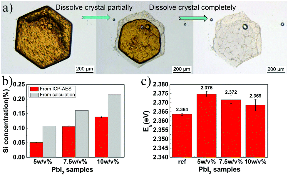 | ||
| Fig. 1 (a) The OM image of PbI2 crystals grown from silica gels (5% w/v) before (left), during (middle) and after (right) dissolution of the crystals; (b) mass ratio of Si in PbI2 crystals grown from silica gels with varied concentrations; and (c) Eg value of referenced PbI2 and PbI2 crystals grown from silica gels with varied concentrations. Ref: reference, PbI2, 99.999%, beads, purchased from Sigma. | ||
The gel-incorporation suggests a possible band gap shift that has been reported for ZnO crystals with incorporated amino acid molecules.27 We next characterized the DRS of the PbI2 powder and then determined the optical band gap value using the Tauc equation combined with the KM method. For more details of band gap measurement, refer to the experimental section.
According to the measured Eg value illustrated in Fig. 1c, the band gap of PbI2 clearly increased after gel incorporation as compared to that of the referenced PbI2 without gel-networks. Interestingly, the maximum Eg shift (0.011 eV) is exhibited in the crystals grown from a 5% w/v gel instead of the maximum gel concentration of 10% w/v. With an increase in gel concentration from 5% w/v to 10% w/v, the amount of incorporated gel-networks increases steadily, whereas the Eg value decreases gradually from 2.375 to 2.368 eV. This trend indicates that an increase in the band gap is not directly associated with the amount of the incorporated gel-networks. We envisioned that the Eg shift might be due to the formation of the host/guest interfaces, and it increased with an increase of interfacial area. This hypothesis was further verified by two pieces of supporting evidence.
First, we examined the gel-network surface area accessible to the crystals. According to previous reports,41 silica gel network comprises aggregation of silica particles; this is reconfirmed by imaging the residues of gel-incorporated PbI2 crystal etched by THF for 6 hours (Fig. S2, ESI†). The surface area of the silica particles was calculated, speculating that their shape is spherical with diameter d (nm), as measured by DLS, and average size and polydispersity index (PdI) of colloidal silica particles are listed in Table 1. The relation between the surface area, S (m2 mL−1), and the concentration of SiO2 particles, C (g mL−1), is expressed by the following equation:

| Samples | Hydrodynamic diameter (nm) | PdI | Surface area (m2 mL−1) | |||
|---|---|---|---|---|---|---|
| SiO2 nanoparticles | 44.8 | 44.8 ± 0.1 | 0.043 | 0.044 ± 0.001 | 0.304 | 0.304 ± 0.001 (if C = 5 mg mL−1) |
| 44.7 | 0.045 | 0.305 | ||||
| 44.9 | 0.045 | 0.304 | ||||
| 5% w/v gel | 130.0 | 129.8 ± 0.3 | 0.208 | 0.183 ± 0.023 | 0.297 | 0.297 ± 0.001 |
| 129.9 | 0.164 | 0.297 | ||||
| 129.4 | 0.177 | 0.298 | ||||
| 7.5% w/v gel | 185.2 | 183.5 ± 1.6 | 0.281 | 0.237 ± 0.038 | 0.313 | 0.316 ± 0.003 |
| 182.2 | 0.220 | 0.318 | ||||
| 183.0 | 0.211 | 0.316 | ||||
| 10% w/v gel | 235.5 | 236.6 ± 3.1 | 0.288 | 0.305 ± 0.020 | 0.328 | 0.326 ± 0.004 |
| 240.1 | 0.299 | 0.321 | ||||
| 234.3 | 0.327 | 0.329 | ||||
Second, the interfacial area between PbI2 and SiO2 is directly increased by incorporating silica nanoparticles in addition to the gel-networks; this results in an increase of Eg values. In previous studies,17,43 nanoparticles have been proven to be incorporated, together with gel-networks, into single crystals grown in gel media. This method is used in this study to introduce nanoparticles. Silica nanoparticles have been selected because they are of the same chemical composition as the silica gel networks (Fig. 2a). The DLS measurement shows that the average diameter of the SiO2 nanoparticles used herein is about 44.8 nm, and the surface area of 5 mg mL−1 SiO2 nanoparticles is up to 0.304 m2 mL−1, which is comparable to that of 5% w/v gel (Table 1). In other words, it is effective to expand the interfacial area by incorporation of additional silica nanoparticles. After obtaining the PbI2 crystal grown from 5% w/v gel containing 5 mg mL−1 SiO2 nanoparticles, EDX and Si element mapping were used to examine the distribution of the Si element. For the as-grown crystal, the Si element mapping indicates almost no contrast between the crystal and the background (Fig. 2b). In contrast, the element mappings show clear signals of the Si element for the slightly etched crystals (Fig. 2c). The discrepancy indicates that silica is incorporated inside the crystal rather than being just adsorbed on the crystal surface. ICP-AES shows that the silica amount in the crystals is higher than that in the crystals grown from gels with the same gel concentration but without silica nanoparticles (Fig. 3b); this is indicative of the incorporation of both silica nanoparticles and gel networks. Correspondingly, the amount of the nanoparticles in the crystals increases from 0 to 0.041% with an increase in the used nanoparticle concentrations from 0 to 5 mg mL−1. Despite the presence of the nanoparticles and gel-networks, the PbI2 crystalline components still exhibit single-crystal nature, as shown by the single set of diffraction spots in the SAED pattern (Fig. 2d). Interestingly, the incorporation of nanoparticles leads to an increase in the Eg values of the PbI2 crystals from 2.375 to 2.386 eV as the concentration of the used nanoparticles increase from 0 to 5 mg mL−1 (Fig. 3a).
 | ||
| Fig. 2 (a) Schematic of crystallization of PbI2 in gel media containing dispersed nanoparticles; (b and c) SEM images and EDX maps (I and Si element) of PbI2 crystal grown from 5% w/v gel containing 5 mg mL−1 SiO2 nanoparticles: (b) as-grown; (c) slightly etched; and (d) SAED of PbI2 grown from 5% w/v gel containing 5 mg mL−1 SiO2 nanoparticles obtained from an illuminated area of 3 μm, indicating the single-crystal nature of the sample. | ||
 | ||
| Fig. 3 (a) Eg value of the PbI2 crystals grown from 5% w/v silica gels with varied concentrations of nanoparticles; (b) mass ratio of Si in PbI2 crystals grown from 5% w/v silica gels with varied concentrations of nanoparticles. The dash line shows Si mass ratio as no nanoparticles are added. While 1 mg mL−1 and 5 mg mL−1 of nanoparticles are added, extra Si (0.019% and 0.041%) is introduced into the crystals. | ||
Based on the abovementioned two experiments and detailed results, we conclude that the PbI2 band gap increases with an increase in the host(crystal)/guest(gel-network and nanoparticles) interfaces. The mechanism of this band gap engineering is attributed to the electrostatic interaction of the iodine 5pz electron in the crystal host and the dipole moment of hydroxyl groups in the gel-network guest. This explanation is consistent with the previous studies on the effect of intercalation on the PbI2 band gap.44,45 PbI2 is a layered-structured material. Guest molecules, including aniline,44 hydrazine,45,46 poly(vinyl alcohol), and polyacrylamide,47 are easily introduced into the interlayer space by intercalation. Interestingly, intercalation often leads to a large increase in band gap (e.g., above 0.5 eV), and calculation of the band structure indicates that the electrostatic interaction between the dipole in the guest and the iodine 5pz electron in the host is very effective in lowering the energy of the upper valence band; this results in an increase in the Eg.44 Instead of intercalation, in this study, polar hydroxyl groups are introduced into PbI2 by a silica gel network and nanoparticle incorporation, and the resulting electrostatic interaction between the hydroxyl groups and the iodine 5pz electron leads to the Eg shift. As a supporting evidence, we introduced an amino group into the gel-networks to replace part of the hydroxyl groups, and the obtained crystals exhibited increased Eg with an increase in the amino group amount. Amino-substituted siloxane (APTMS) was used as a co-precursor with TMOS for gelation; thus, the amino groups were introduced (Fig. 4a). Because the O-, S-, and N-donor ligands tend to coordinate with the lead atom of lead halides48 and the amino group has a stronger basicity, the amino group should be closer to the PbI2 host system; this results in the dipole moment of the amino group located on the surface of silica gels having stronger electrostatic interaction with PbI2 crystal host as compared to that of the hydroxyl group. The gel concentration was fixed at 10% v/v with varied CNH2 of 2.5%, 5%, and 7.5%. The crystals grown from amino-modified silica gels were confirmed to be PbI2via PXRD (Fig. S1, ESI†). Similar to that observed before, when the gel-grown crystal was partially and completely dissolved, translucent residual silica gels were left with almost the same shape as that of the original PbI2 crystal (Fig. 4b–e). This result proves the incorporation of these four types of gels. It is worth noting that the shape of the crystal changes as the amino groups are introduced; this indicates that the amino groups located on the surface of incorporated silica gels have a strong interaction with the PbI2 crystal host. Then, we estimated the band gap of these PbI2 crystals using DRS. The Eg value was significantly increased after gel incorporation, and there was a positive correlation between the band gap value and the proportion of the amino groups CNH2 (Fig. 5a). The largest band gap shift was 0.025 eV from 2.364 eV of the referenced PbI2 to 2.389 eV of the PbI2 crystals grown from 10% v/v gel with CNH2 of 7.5%. ICP-AES shows that the amounts of incorporated Si element inside the crystals grown from the gel without amino groups were much lower than the calculated content; amino-modified gel incorporated crystals, however, show high incorporating efficiency (Fig. 5b). This result indicates that silica gel networks prepared from alkoxide are weaker than those prepared from Na2SiO3,49 and the introduction of amino groups enhances the affinity between the gel guest and crystal host. The mass ratio of the incorporated Si element inside the crystals is calculated from the equation20 proposed earlier. Therefore, marked shifts in the band gap are achieved by introducing an amino group into silica gels due to increased interatomic forces (electrostatic interaction) at the host/guest interfaces.
 | ||
| Fig. 4 (a) The chemical structures of the two precursors (TMOS and APTMS) and the corresponding gels; (b–e) OM images obtained during the dissolution processes of PbI2 crystals grown from 10% v/v silica gels with 0% NH2 (b), 2.5% NH2 (c), 5% NH2 (d), and 7.5% NH2 (e). | ||
 | ||
| Fig. 5 (a) Eg value of the referenced PbI2 and PbI2 crystals grown from 10% v/v silica gels with varied proportion of amino groups; (b) mass ratio of Si in PbI2 crystals grown from 10% v/v silica gels with varied proportion of amino groups. | ||
In addition, another possible explanation of the Eg shift might be associated with the lattice strain induced by gel incorporation. In the intercalated PbI2, a quite noticeable lattice expansion (3 Å) along the c-axis of the crystal host plays a minor role in band gap increase apart from the electrostatic interaction.44–46 Similarly, for another semiconducting material, ZnO crystals, incorporation of amino acid molecules induces lattice strains and changes the band gap of the semiconductor host.27 In our present study, PXRD combined with the Rietveld refinement method was performed to deduce the lattice parameters of PbI2, but the overall lattice strain was too small to be accurately characterized (Table S2, ESI†).
Based on these observations, we proposed the following explanations for the band gap shift of gel-incorporated PbI2. Silica gels became incorporated inside PbI2 single crystals grown through the gel method without disturbing the long-range order (single-crystallinity), but introduced large areas of crystal-host/gel-guest interfaces. Owing to the electrostatic interaction between the iodine electron of PbI2 host and the dipole moment of hydroxyl groups located on the surface of gels, a clear increase of band gap occurred. With the increasing gel concentration, band gap shift was not enlarged because the area of the host/guest interfaces was not expanded. When additional silica nanoparticles were introduced inside the crystal with gels, band gap shift was enlarged with the increasing quantity of incorporated nanoparticles because of the expanded area for the interatomic forces (electrostatic interaction) at the interfaces. Additional support for this idea was that a larger band gap shift was caused after we enhanced the interatomic forces at the host/guest interfaces by introducing amino groups into silica gels.
Conclusions
In summary, we have demonstrated that the band gap of gel-grown PbI2 crystals can be increased by incorporating a gel-network guest into the crystal host. The mechanism of band gap shift is attributed to the electrostatic interaction at the host/guest interfaces. The shift amount increases with an increase in the host/guest interfacial area as well as the host/guest electrostatic interaction, with the largest Eg shift being 0.025 eV, as compared to the case of the crystals without gel incorporation. Although the overall shift is smaller than that observed in the traditional strategies of band gap engineering, having another avenue that can be added to or combined with these methods may be a better choice because this bio-inspired route has an advantage of low-temperature solution-processing ability.Conflicts of interest
There are no conflicts of interest to declare.Acknowledgements
This work was supported by the 973 Program (2014CB643503), National Natural Science Foundation of China (51625304, 51373150, 51461165301).Notes and references
- J. Aizenberg, J. Hanson, T. Koetzle, S. Weiner and L. Addadi, J. Am. Chem. Soc., 1997, 119, 881–886 CrossRef CAS.
- J. Aizenberg, D. A. Muller, J. L. Grazul and D. Hamann, Science, 2003, 299, 1205–1208 CrossRef CAS PubMed.
- J. Aizenberg, A. Tkachenko, S. Weiner, L. Addadi and G. Hendler, Nature, 2001, 412, 819–822 CrossRef CAS PubMed.
- F. Nudelman, H. H. Chen, H. A. Goldberg, S. Weiner and L. Addadi, Faraday Discuss., 2007, 136, 9–25 RSC.
- Y. Politi, T. Arad, E. Klein, S. Weiner and L. Addadi, Science, 2004, 306, 1161–1164 CrossRef CAS PubMed.
- J. Robach, S. Stock and A. Veis, J. Struct. Biol., 2005, 151, 18–29 CrossRef CAS PubMed.
- M. D. Giosia, I. Polishchuk, E. Weber, S. Fermani, L. Pasquini, N. M. Pugno, F. Zerbetto, M. Montalti, M. Calvaresi and G. Falini, Adv. Funct. Mater., 2016, 26, 5569–5575 CrossRef.
- S. Ludwigs, U. Steiner, A. N. Kulak, R. Lam and F. C. Meldrum, Adv. Mater., 2006, 18, 2270–2273 CrossRef CAS.
- Y. Ning, L. A. Fielding, L. P. Ratcliffe, Y.-W. Wang, F. C. Meldrum and S. P. Armes, J. Am. Chem. Soc., 2016, 138, 11734–11742 CrossRef CAS PubMed.
- R. J. Park and F. C. Meldrum, Adv. Mater., 2002, 14, 1167–1169 CrossRef CAS.
- R. J. Park and F. C. Meldrum, J. Mater. Chem., 2004, 14, 2291–2296 RSC.
- A. S. Schenk, I. Zlotnikov, B. Pokroy, N. Gierlinger, A. Masic, P. Zaslansky, A. N. Fitch, O. Paris, T. H. Metzger and H. Cölfen, Adv. Funct. Mater., 2012, 22, 4668–4676 CrossRef CAS.
- A. Patel and A. V. Rao, Bull. Mater. Sci., 1982, 4, 527–548 CrossRef CAS.
- H. Nickl and H. Henisch, J. Electrochem. Soc., 1969, 116, 1258–1260 CrossRef.
- J. A. Gavira and J. M. García-Ruiz, Acta Crystallogr., Sect. D: Biol. Crystallogr., 2002, 58, 1653–1656 CrossRef.
- J. M. Garcıa-Ruiz, J. A. Gavira, F. Otálora, A. Guasch and M. Coll, Mater. Res. Bull., 1998, 33, 1593–1598 CrossRef.
- Y. Liu, W. Yuan, Y. Shi, X. Chen, Y. Wang, H. Chen and H. Li, Angew. Chem., Int. Ed., 2014, 53, 4127–4131 CrossRef CAS PubMed.
- H. Li, H. L. Xin, D. A. Muller and L. A. Estroff, Science, 2009, 326, 1244–1247 CrossRef CAS PubMed.
- W. Liu, Y.-J. Liu, L. Chen, T. Ye, H.-Z. Chen and H.-Y. Li, Chin. Chem. Lett., 2015, 26, 504–508 CrossRef CAS.
- J. Ren, B. Huang, L. Chen, Y. Liu, T. Ye, W. Liu, X. Jin, Z.-K. Xu, H. Chen and H. Li, CrystEngComm, 2016, 18, 800–806 RSC.
- Y. Liu, H. Zang, L. Wang, W. Fu, W. Yuan, J. Wu, X. Jin, J. Han, C. Wu and Y. Wang, Chem. Mater., 2016, 28, 7537–7543 CrossRef CAS.
- G. Yu, J. Gao, J. C. Hummelen, F. Wudl and A. J. Heeger, Science, 1995, 270, 1789–1791 CAS.
- J. J. M. Halls, C. A. Walsh, N. C. Greenham, E. A. Marseglia, R. H. Friend, S. C. Moratti and A. B. Holmes, Nature, 1995, 376, 498–500 CrossRef CAS.
- K. S. Park, J. Baek, Y. Park, L. Lee, J. Hyon, Y.-E. K. Lee, N. K. Shrestha, Y. Kang and M. M. Sung, Adv. Mater., 2017, 29, 1603285 CrossRef PubMed.
- J. Wu, Q. Li, G. Xue, H. Chen and H. Li, Adv. Mater., 2017, 29, 1606101 CrossRef PubMed.
- A. Brif, L. Bloch and B. Pokroy, CrystEngComm, 2014, 16, 3268–3273 RSC.
- A. Brif, G. Ankonina, C. Drathen and B. Pokroy, Adv. Mater., 2014, 26, 477–481 CrossRef CAS PubMed.
- R. Muñoz-Espí, Y. Qi, I. Lieberwirth, C. M. Gomez and G. Wegner, Chem. – Eur. J., 2006, 12, 118–129 CrossRef PubMed.
- R. Muñoz-Espí, A. Chandra and G. Wegner, Cryst. Growth Des., 2007, 7, 1584–1589 Search PubMed.
- A. N. Kulak, R. Grimes, Y.-Y. Kim, M. Semsarilar, C. Anduix-Canto, O. Cespedes, S. P. Armes and F. C. Meldrum, Chem. Mater., 2016, 28, 7528–7536 CrossRef CAS.
- C. Lu, L. Qi, H. Cong, X. Wang, J. Yang, L. Yang, D. Zhang, J. Ma and W. Cao, Chem. Mater., 2005, 17, 5218–5224 CrossRef CAS.
- A. E. DiCorato, E. Asenath-Smith, A. N. Kulak, F. C. Meldrum and L. A. Estroff, Cryst. Growth Des., 2016, 16, 6804–6811 CAS.
- L. Chen, I. Polishchuk, E. Weber, A. N. Fitch and B. Pokroy, Cryst. Growth Des., 2016, 16, 2972–2978 CAS.
- G. Ou, D. Li, W. Pan, Q. Zhang, B. Xu, L. Gu, C. Nan and H. Wu, Adv. Mater., 2015, 27, 2589–2594 CrossRef CAS PubMed.
- F. Capasso, Science, 1987, 235, 172–176 CAS.
- A. W. Fountain III, N. J. Withers, P. J. Gardner, B. A. Akins, A. C. Rivera, J. B. Plumley, G. A. Smolyakov and M. Osiński, SPIE, 2009, 7304, 73041N CrossRef.
- A. Schwartz and J. C. Oconnell, J. Electrochem. Soc., 1973, 120, 697–698 CrossRef CAS.
- A. Ferreira da Silva, N. Veissid, C. Y. An, I. Pepe, N. Barros de Oliveira and A. V. Batista da Silva, Appl. Phys. Lett., 1996, 69, 1930–1932 CrossRef CAS.
- R. López and R. Gómez, J. Sol-Gel Sci. Technol., 2011, 61, 1–7 CrossRef.
- H. Sun, X. Zhu, D. Yang, J. Yang, X. Gao and X. Li, Phys. Status Solidi A, 2014, 211, 823–827 CrossRef CAS.
- A. V. Rao, G. Pajonk, U. K. Bangi, A. P. Rao and M. M. Koebel, Aerogels Handbook, Springer, 2011, pp. 103–124 Search PubMed.
- C. J. Kiely, J. Fink, M. Brust, D. Bethell and D. J. Schiffrin, Nature, 1998, 396, 444–446 CrossRef CAS.
- Y.-Y. Kim, A. S. Schenk, D. Walsh, A. N. Kulak, O. Cespedes and F. C. Meldrum, Nanoscale, 2014, 6, 852–859 RSC.
- V. Mehrotra, S. Lombardo, M. O. Thompson and E. P. Giannelis, Phys. Rev. B: Condens. Matter Mater. Phys., 1991, 44, 5786–5790 CrossRef CAS.
- R. Aljishi, C. C. Coleman, R. Treece and H. Goldwhite, Phys. Rev. B: Condens. Matter Mater. Phys., 1989, 39, 4862–4865 CrossRef CAS.
- C. C. Coleman, B. Magness, P. Melo, H. Goldwhite, W. Tikkanen, Q. Tham, K. Pham, R. Jacubinas, R. B. Kaner and R. E. Treece, J. Phys. Chem. Solids, 1996, 57, 1153–1158 CrossRef CAS.
- N. Preda, L. Mihut, M. Baibarac, I. Baltog and S. Lefrant, J. Phys.: Condens. Matter, 2006, 18, 8899–8912 CrossRef CAS.
- L. C. Yuhallada and A. H. Francis, J. Phys. Chem., 1990, 94, 7518–7523 CrossRef CAS.
- H. Li and L. A. Estroff, Adv. Mater., 2009, 21, 470–473 CrossRef CAS.
Footnote |
| † Electronic supplementary information (ESI) available: PXRD patterns and lattice parameters of PbI2, SEM image and size of silica particles derived from DLS measurements, the original measured data by DRS. See DOI: 10.1039/c7qm00509a |
| This journal is © the Partner Organisations 2018 |