
Electrolyte-gated light-emitting transistors: working principle and applications
Jiang
Liu
 a,
Fangchao
Zhao
a,
Huaping
Li
*b and
Qibing
Pei
*a
a,
Fangchao
Zhao
a,
Huaping
Li
*b and
Qibing
Pei
*a
aDepartment of Materials Science and Engineering, University of California Los Angeles, 420 Westwood Plaza, Los Angeles, CA 90095, USA. E-mail: qpei@seas.ucla.edu
bAtom Nanoelectronics Inc., 440 Hindry Avenue, Unit E, Inglewood, CA 90301, USA. E-mail: huaping.li@atomnanoelectronics.com
First published on 13th November 2017
Abstract
Adding solid electrolytes into organic semiconductors broadens the scope of material properties and electronic applications. Successful examples include polymer light-emitting electrochemical cells, electrolyte-gated organic transistors, and electrolyte-gated organic light-emitting transistors (EGLETs). EGLETs combine an organic light-emitting device and a transistor with a high capacitance electrolytic dielectric. Here we summarize recent progress in the development of EGLETs in both planar and vertical device architectures. The former offers a lateral geometry and in-plane light-emission for scientific scaffolds in the fundamental study of organic semiconductor opto-physics. The latter features surface emission with a unity aperture ratio, and it can be used in matrix displays without the requirement of external thin-film transistor arrays as the switching circuitry. This strategy paves an easy avenue towards fabricating highly integrated organic optoelectronic devices, and it offers a new test bed for research in iontronics and organic electronics.
 Jiang Liu | Jiang Liu has been a postdoctoral researcher in the Soft Materials Research Lab of the University of California, Los Angeles, since September, 2014. His research is focused on light emitting transistors, AMOLED driving, flexible OLEDs and other organic electronic devices/systems. Prior to joining UCLA, Jiang Liu received his PhD in Organic Electronics from Linköping University of Sweden, and BS in Electrical Engineering from Southeast University of China. |
 Fangchao Zhao | Fangchao Zhao received his PhD degree in Polymer Chemistry and Physics from Changchun Institute of Applied Chemistry, the Chinese Academy of Sciences in 2012, and then he joined Harbin Oshine Photoelectric Technology Co., LTD as the R&D manager working with white organic light-emitting diodes for lighting application. Currently, he is a postdoctoral research fellow at the University of California Los Angeles, focusing on organic and polymer optoelectronic devices. |
 Huaping Li | Huaping Li is the Chief Scientist at ATOM Nanoelectronics in charge of company operation, hiring and management, and technical challenges. He raised and managed over $1M government funded projects through DoD and NSF. His research focuses on carbon nanotube separation, carbon nanotube thin film transistor fabrication, printed electronics, advanced materials and gated OLED fabrication for emerging displays. He received his BS from HuBei University in 1995 and MS from the Chinese Academy of Sciences in 1998. Dr Li was graduated from Clemson University with PhD in Organic Chemistry in 2006, and trained as a postdoctoral researcher at UCSB. |
 Qibing Pei | Qibing Pei is a Professor of Materials Science and Engineering at the University of California, Los Angeles, and directs the UCLA Soft Materials Research Lab. He specializes in synthetic polymers and composites for electronic, electromechanical, and photonic applications, with over 180 journal publications and 43 issued US patents. He received a BS from Nanjing University and PhD from the Institute of Chemistry, the Chinese Academy of Sciences. He is a Fellow of SPIE, member of ACS and MRS, Associate Editor of Smart Materials & Structures and Soft Robotics, and Advisory Board Member of Advanced Electronic Materials and Scientific Reports. |
Organic semiconductors augmented with solid electrolytes
Organic semiconductors are fascinating materials with electrical and optical properties closely related to their molecular structure. This feature, together with their mechanical flexibility and low-cost processability, makes organic semiconductors versatile candidates for various electronic applications. As the most developed organic electronic technology, organic light-emitting diodes (OLEDs), are already on the market in high-end displays for mobile phone devices and television sets.1 State-of-the-art OLED devices are fabricated by sequentially evaporating 7–9 different layers of organic molecules under vacuum.2 In order to inject electrons efficiently into the organic materials, low work function metals or injection interfacial layers such as lithium fluoride or cesium carbonate are commonly used.3,4 All of these materials are air-sensitive, and they require rigorous and expensive encapsulations.5 This remains a key factor in the high cost of OLED displays, which limits the market viability of organic electronic technology.Polymer light-emitting electrochemical cells (LECs) were invented in 1994 to mitigate the charge injection problem in organic optoelectronics.6 In the LEC materials system, a solid electrolyte is blended with an organic semiconductor. The presence of ions electrochemically-dopes the semiconductor and facilitates the electron injection without using air-sensitive materials. In fact, electrons could be effectively taken from a stable metal like gold or silver and injected into the lowest, unoccupied molecular orbital of an organic semiconductor,7–10 which is usually 1–2 eV higher than the metal's work function.
LECs are promising candidates for next-generation solid-state lighting and display applications, as they possess several unique properties. First, an efficient charge injection at the electrodes arises from the existence of ions at the interface, and it is insensitive to the work function of the electrodes. Thus, any conductive material can be used as an electrode, varying from stable, high work function metals (Au, Ag and Al) and organic conductors, to graphene and commonly used transparent indium-tin-oxide.11–15 Second, the electrochemical process in an LEC is largely independent of the cathode–anode distance. Therefore, variation in film thickness and roughness is less impactful in large area roll-to-roll processes.16 As a result, LECs are sufficiently robust for stretchable and flexible electronic applications.13,16–19 In addition to the applications in optoelectronic device, solid electrolytes have potential as dielectric materials in transistors due to their high capacitance20 (see Fig. 1a). The transistor drain current equation is presented as:

 | ||
| Fig. 1 (a) An electrolyte-gated organic transistor with a planar source and drain. The emissive p–n junction is part of the channel. (b) A vertical electrolyte-gated light-emitting transistor with surface emission. The porous source electrode is an important attribute for the device operation. | ||
Organic light-emitting transistors (LETs) represent a novel class of organic optoelectronic devices, wherein the light-emission function of an OLED and the electrical-modulation function of a transistor are inherently combined.30–35 LETs offer higher charge carrier mobilities36,37 over OLEDs and in situ color tuning functionalities.38,39 Conventional LETs are usually gated by inorganic dielectrics, such as aluminum oxide or silicon oxide.31 Solid oxide dielectrics formed by atomic layer deposition or chemical vapor deposition offer high dielectric constants, but their deposition is expensive. Moreover, LETs require ultra-thin dielectrics for low voltage operation, which increases their fabrication complexity. For more information, a detailed review of LET devices has been published elsewhere.31
Combining the high capacitance value of the electrolyte in an EGT configuration and its ability to dope organic semiconductor properties in LECs, an electrolyte-gated light-emitting transistor (EGLET) was proposed and developed. This review will discuss the materials, working mechanisms, device performance, and its applications in organic optoelectronics.
Electrolyte-gated light-emitting transistors: the basics
As mentioned earlier, OLED displays provide superior picture quality compared with their LCD counterparts. Thanks to their self-emissive characteristics, OLED displays offer high contrast, large viewing angles, a wide color gamut, and fast response times. Nevertheless, OLED displays, usually in the form of active-matrix OLED (AMOLED), require field-effect transistors to switch their electroluminescence intensity, which are complex to fabricate.40 In fact, each pixel in an AMOLED display needs at least two thin-film transistors (TFT) and one capacitor driving and switching control (2T1C) to achieve stable and uniform light output.41,42 The fabrication of a transistor backplane is complicated and expensive, and their rigidity disqualifies them for flexible displays.EGLETs include the switching functions of a transistor and the light-emitting abilities of an OLED (or an LEC). Therefore, no additional driving transistors are needed when EGLETs are employed in a display matrix, which provides a method to realize highly-integrated optoelectronic applications. In contrast to the rigid dielectric materials used in conventional OLEDs or LETs, EGLETs use solution-processed electrolytes as the dielectric layer, which permits fully printable and flexible optoelectronics applications.
Structure
In terms of the structure, an EGLET is usually a three-terminal device, with terminals denoted as the drain, source, and gate, as shown in the planar structure in Fig. 1a. An organic emissive layer (EML) is placed between the drain and source electrodes, which emits light once a sufficient voltage is applied across it. On top of the EML there is a gate electrode, which is isolated from the EML by an electrolyte dielectric layer. As depicted in Fig. 1b, the EGLETs can also be vertically structured, and they are usually built on a transparent electrode (drain) with bottom emission. On top of the electrode is a vertical OLED stack with a porous source electrode. An electrolytic dielectric makes contact with the EML through the porous source layer, which is modulated by the topmost gate electrode. In both structures, the gate controls the amount of light emitted from the device and/or the spatial light emitting position. This electrolyte-gated lighting modulation is the key characteristics of EGLET devices; the mechanism will be discussed below.Working principle
The working principle of planar EGLETs is shown in Fig. 2.43 When the gate is inactive (Fig. 2a), the planar EGLET is similar to a planar bilayer LEC device.44 Once a voltage is applied between the cathode and the anode, the resultant electric field forces the anions and cations to drift in opposite directions, and form pairs with the opposing-charged charge carriers, forming electric double layer capacitors45 (EDLCs) at the metal/organic interface. EDLCs usually have only a thickness of 1–5 nm,46 leading to a strong interfacial electric field across the metal and the organic material. This electric field results in steep band bending at the metal/organic interface, and Schottky barrier narrowing. Because of this, the charge carriers are injected into the organic semiconductor by the tunneling effect.47 Hence, holes are injected from the anode and electrons from the cathode into the EML. The light emitting polymer (LEP) near the anodic interface is then oxidized (p-doped), and the polymer near the cathode is reduced (n-doped). The counter ions in the electrolyte dissociate and migrate towards the electrodes to compensate for the injected charges, and as a result, the redox composites of LEP/hole/anion (or LEP/electron/cation) are neutralized and stabilized, following the reaction below:| n-doping: P0 + e− + C+ → P−C+ |
| p-doping: P0 + h+ + A− → P+A− |
 | ||
| Fig. 2 Operation principles of an EGLET. (a) The emissive p–n junction is formed in the LEP channel due to charge injection from the planar source (cathode) and drain (anode) electrodes. (b) Positive gate voltage introduces excess positive charge into the channel and effectively shifts the emission zone towards the anode. (c) Similarly, a negative gate voltage shifts the p–n junction towards the cathode. Reprinted with permission from ref. 43. Copyright 2005 Wiley-VCH. | ||
Since the doped LEP is a good electric conductor, it serves as an extension of the charge-injection electrodes. As the n- and p-doped polymer regions expand towards the center, the intrinsic LEP region in the middle shrinks in size. After the central intrinsic LEP is reduced to a point where the electrons and holes injected from the doped polymer are close enough to recombine, excitons are formed. The excitons will decay to generate light radiatively or heat non-radiatively.
When a positive gate voltage is applied with reference to the cathode (Fig. 2b), an electric potential is generated across the electrolyte dielectric, forcing the anions to drift towards the gate and the cations towards the EML. The cations enhance the n-doped area in the EML, and the emissive p–n junction would move towards the anode. Likewise, a negative gate voltage would drive the anions towards the EML, enlarging the p-doped region and de-doping the n-doped region. As a result, the lighting position move towards the cathode (Fig. 2c).
Since both n-doping and p-doping increase the conductivity of the EML, the channel current flowing between the drain and the source increases under the applied gate voltage. This gate-modulated current change by electrochemical doping is analogous to those in organic electrochemical transistors.48,49 An increase in the channel conductivity also improves electron and hole injection into the channel, generating even more photons.
Materials
The key materials in the EGLETs are electrolytes and emissive materials. Table 1 summarizes the typical electrolytes and emissive materials used in EGLETs.| Structure | Dielectric | Emission layer | Voltage level (V) | I on/off | L on/off | L max (cd m−2) | Ref. |
|---|---|---|---|---|---|---|---|
| Planar | SiO2 | SY:DCH18C6:LiTf | 40 | 3 | N/A | N/A | 53 |
| Planar | SiO2 and PEO:LiTf | Tetracene | 10 | ∼10 | ∼10 | N/A | 54 |
| Planar | Polyvinyl alcohol | MDMO-PPV:PEO:LiTf | 50 | ∼800 | N/A | N/A | 55 |
| Planar | BCB | MDMO-PPV:PEO:LiTf | 50 | 5 | N/A | N/A | 56 |
| Planar | PEO:LiTf | MEH-PPV | 5 | 100 | N/A | N/A | 43, 57 and 58 |
| Planar | EMIM-TFSI | F8BT | 3 | 107 | N/A | N/A | 59 |
| Vertical | PEO:LiTf:PMMA | SY | 8 | ∼100 | 103 | 8000 | 60,61 |
| Vertical | PEO:LiTf:PMMA | A white emitting polymer | 8 | ∼100 | 103 | 6000 | 62 |
| Vertical | PEO:LiTf:PMMA | CBP: iridium dopant | 8 | ∼100 | 105 | 104 | 63 |
The desired properties of electrolytes are (1) high ion conductivity, which provides a low voltage operation and a fast device response, and (2) high electrical resistivity, which is necessary to minimize the gate leakage current. Commonly-used electrolytes include polymer electrolytes and ionic liquids; see Fig. 3.
 | ||
| Fig. 3 Chemical structures of the components of the solid electrolytes used in the EGLETs. (a) Polymer electrolytes consist of an inorganic salt LiCF3SO3 dissolved in an ion coordinating polymer PEO; (b) ionic liquids usually possess a higher ionic conductivity than polymer electrolytes, since they are in a molten state at room temperature and do not require an extra ion conductor such as PEO. Here is an example of an ionic liquid: EMIM:TFSI. | ||
Polymer electrolytes consist of an inorganic salt (e.g. LiCF3SO3) dissolved in an ion coordinating polymer (poly(ethylene oxide) (PEO)), as shown in Fig. 3a. In this electrolyte, the repeating oxygen groups in the PEO chains are strong electron donors, which form a strong coordination bond with the cations. Since PEO possesses a low glass transition temperature of around −65 °C, the PEO chains are fairly flexible at room temperature, and thus allow the ions to move in the PEO matrix.50
Ionic liquids usually possess a higher ionic conductivity than polymer electrolytes, since they are in a molten state at room temperature and do not require an extra ion conductor such as PEO. However, their liquid nature limits their practical applications.51 A small amount of gelation agent is usually added to improve their mechanical integrity.52Fig. 3b displays a typical ionic liquid 1-ethyl-3-methyl imidazolium bis(trifluoromethyl sulfonyl)imide (EMIM:TFSI).
The emissive layer materials of EGLET devices are typically polymers or small molecules; see Fig. 4. To realize the functions of EGLET, (1) EMLs need to be efficient emitters, and (2) they must possess the electrochemical capacity to be reversibly doped by the electrolyte of the system.
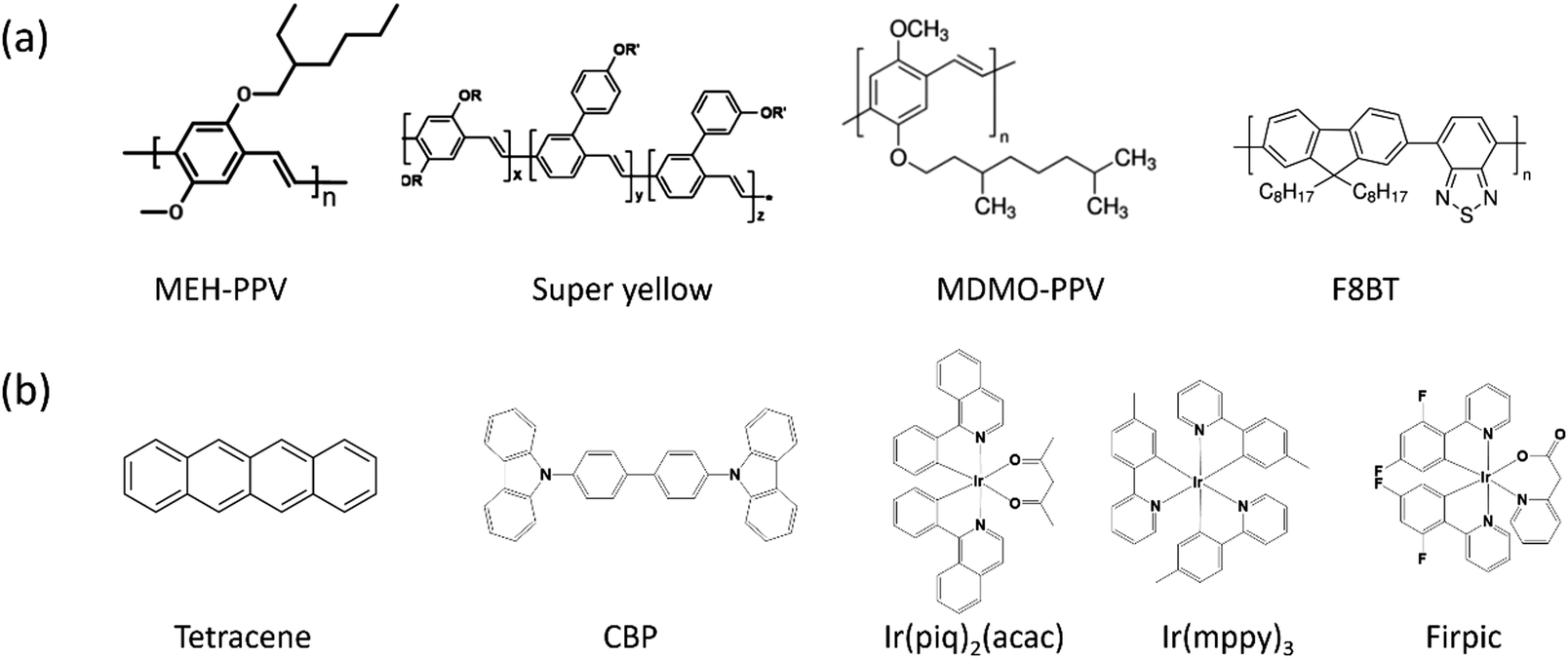 | ||
| Fig. 4 Chemical structures of the luminescent emitters used in the EGLET devices. (a) Conjugated polymer emitters. All are fluorescent light emitting polymers. (b) Small molecule emitters. Tetracene and CBP are fluorescent emitters, while Ir(piq)2(acac), Ir(mppy)3 and Firpic are phosphorescent emitters. | ||
Polymer emitters (Fig. 4a) are more attractive than evaporated small molecules in practical applications, because they can be solution-processed (potentially printable), and they are intrinsically flexible. The polymer materials reported in the EGLET publications include: poly[2-methoxy-5-(2-ethylhexyloxy)-1,4-phenylenevinylene] (MEH-PPV) and poly[2-methoxy-5-(3′,7′-dimethyloctyloxy)-1,4-phenylenevinylene] (MDMO-PPV), super-yellow (SY), poly(9,9′-dioctylfluorene-co-benzothiadiazole) (F8BT), and a white emitting polymer with an unlisted structure.
Small molecules (Fig. 4b) are the preferred emitters in current OLEDs partially because of the availability of high purity compounds by repeated sublimation.64 Moreover, the use of high vacuum physical vapor deposition systems allows the formation of multiple ultrathin layers of organic small molecules to precisely manipulate the charge carriers and excitons. However, small molecules are easily washed away when an electrolyte solution is cast onto them. The incompatibility between the small molecules and solution processed electrolyte results in the fact that they are sporadically explored in EGLETs. Examples of a small molecule EML used in EGLETs include tetracene,65 and a mixture of CBP ((4,4-bis(N-carbazolyl)-1,1-biphenyl)) host doped with iridium-containing phosphorescent guests.66
Demonstrations of EGLET devices and their applications
Planar devices
The first attempt to employ an electrolyte as the dielectric in an organic light-emitting transistor dates back to 200554 by Hepp and coworkers. As depicted in Fig. 5a, the transistor features a bottom gate structure. Above the Si gate, there is a bi-layer dielectric consisting of SiO2 and a polymer electrolyte. Gold is used as the drain and the source, and tetracene with a thickness of 100 nm forms the EML. The polymer electrolyte is a mixture of poly(ethylene-oxide) and lithium triflate (LiTf) in a weight ratio of 3![[thin space (1/6-em)]](https://www.rsc.org/images/entities/char_2009.gif) :1. At a constant VDS of 10 V, the light emission, characterized by the photocurrent in a photodiode, is modulated by different gate voltages, as seen in Fig. 5b. As VGS increases from 0 V to 10 V, the photocurrent increases by a factor of 8. The author attributes this effect to the interfacial electrochemical doping between the polymer electrolyte and tetracene. This is the first light emitting transistor that operates under 10 V, thanks to the high capacitance electrolytic dielectric layer. However, in this structure, there are two capacitors (C1 as the polymer electrolyte and C2 for SiO2) connected in series, so the total capacitance Ctotal = 1/(1/C1 + 1/C2) is limited by the much smaller C2.
:1. At a constant VDS of 10 V, the light emission, characterized by the photocurrent in a photodiode, is modulated by different gate voltages, as seen in Fig. 5b. As VGS increases from 0 V to 10 V, the photocurrent increases by a factor of 8. The author attributes this effect to the interfacial electrochemical doping between the polymer electrolyte and tetracene. This is the first light emitting transistor that operates under 10 V, thanks to the high capacitance electrolytic dielectric layer. However, in this structure, there are two capacitors (C1 as the polymer electrolyte and C2 for SiO2) connected in series, so the total capacitance Ctotal = 1/(1/C1 + 1/C2) is limited by the much smaller C2.
 | ||
| Fig. 5 (a) Structure of the first reported planar EGLET and (b) its electrical and light emission characteristics. The device consists of two layers of dielectric materials: SiO2 and a polymer electrolyte. The light emission intensity increases by 8 times with the gate voltage switching from 0 V to −10 V. The authors performed the experiment at 230 K because the elevated temperature caused the mobile ions to screen the gate potential to a certain extent. Reprinted with permission from ref. 54. Copyright 2005 Wiley-VCH. | ||
Later on, Liu et al. reported a top-gate EGLET.43 Unlike Hepp's work, this device uses a polymer electrolyte as the sole dielectric material, resulting in an operation voltage within 5 V. As depicted in the inset of Fig. 6a, the device possesses a bottom drain and source made of gold. A light-emitting polymer (MEH-PPV) was spin-cast as the channel. The blend of PEO and KCF3SO3 serving as the dielectric was drop-cast before poly(3,4-ethylenedioxythiophene-2,5-diyl):polystyrene sulfonate (PEDOT:PSS) was laminated on top of the electrolyte layer as the gate. The device exhibits clear transistor behavior as shown in the transfer curve in Fig. 6a. It has a current on/off ratio of around 50 when VG sweeps from 0 to −5 V (p-doping). Most interestingly, the light emission zone, which was initially close to the cathode with an inactive gate, moves towards the anode with a positive VG (n-doping) and backwards with a negative VG (p-doping). The spatial control of the emission zone was also reported in a LET structure with an oxide dielectric, working under 100 V.67,68 Here the low voltage operation (<5 V) is again attributed to the high capacitance of the polymer electrolyte and the electrochemical doping between the electrolyte and the polymer emitter.
 | ||
| Fig. 6 (a) Transfer characteristics of the EGLET reported by Berggren's group; the device structure is shown in the inset. (b) Light emission zone is spatially controlled while the device is alternated between n-doping and p-doping operation. Reprinted with permission from ref. 43. Copyright 2011 American Chemical Society. | ||
With a structure similar to that of Liu's work, Bhat et al. reported an EGLET59 using F8BT as the light-emitting polymer, and an ionic liquid EMIM:TFSI as the dielectric. A top gate PEDOT:PSS was drop-cast offset to the channel (Fig. 7a) so that the light emission from the channel is not absorbed by the gate. Unlike conventional transistors, electrolyte gated transistors still function with the gate electrode misaligned with the channel69 because the capacitance of the electrolyte is independent of the electrolyte thickness. The authors observed light emission when Vds was over 3 V. Current modulation with different VG is pronounced (Fig. 7b), but no light modulation is reported. The authors employed charge accumulation spectroscopy (CAS) to study the electrochemical doping. After applying a negative gate voltage, the authors observed significant penetration of negative TFSI ions into the light emitting polymer (p-doping), evidenced by the spectrum change in CAS shown in Fig. 7c. However, they observed no evidence of positive ion diffusion with positive gate voltages (n-doping) (Fig. 7d). This hole-current dominated operation leads to light emission occurring in the proximity of the cathode due to the lack of n-doping. As a result, no gate-modulated spatial modulation was reported.
 | ||
| Fig. 7 (a) The EGLET reported by Sirringhaus's group. The gate electrode is misaligned to the channel, so that the light emission is not absorbed by the gate electrode. (b) The transfer characteristics of the device with clear hysteresis. Charge accumulation spectroscopy (CAS) under (c) negative gate voltages and (d) positive voltages. Upon application of a negative gate voltage, significant spectrum changes in CAS are shown in (c), indicating the penetration of negative TFSI ions into the light emitting polymer (p-doping). A positive gate voltage does not induce a similar spectrum change, suggesting that the positive ions do not penetrate the LEP under this voltage. Reprinted with permission from ref. 59. Copyright 2012 American Chemical Society. | ||
Two major light-emitting polymers employed in the previously mentioned EGLET devices, PPV and F8BT, have been intensively studied under the electrolyte gating configuration by different groups of researchers.22,70–72 Although no light-emitting properties were studied, they thoroughly investigated the electrical property modulation of these LEPs in ionic environments. Frisbie's group used the ionic liquid 1-ethyl-3-methylimidazolium tris(pentafluoroethyl)trifluorophosphate (EMI-FAP) to gate both F8BT and MEH-PPV, with a top Pt gate configuration as shown in Fig. 8a. The conductivities of both the polymers were modulated by electrochemical p-doping as a function of the gate potential in a transistor geometry. In these experiments, very high carrier densities on the order of 1021 cm−3 were obtained in the polymer semiconductors with ionic liquid gating. Interestingly, the polymers displayed a non-monotonic conductivity dependence on the different gate potentials, as shown in Fig. 8b and c. The conductivity initially increases as the potential increases, followed by a peak and an eventual decrease as the doping potential increases. The authors claim that this reversible decrease results from a hole mobility dependent on the carrier density. In a similar experiment, Sayago and coworkers used three ionic liquids containing TFSI anions to gate MEH-PPV.72 Under a drain–source voltage of 1 V, a 103 on–off drain–source current ratio was observed when the gate was swept from 0 V to 1 V because of p-doping electrochemical reactions between MEH-PPV and TFSI. Both Frisbie and Sayago's experiments focus on p-doping of the polymers, but they did not report n-doping of the transistors.
 | ||
| Fig. 8 (a) Experimental setup for hole transport property study of F8BT and MEH-PPV under ionic liquid gating. Measured hole current for (b) F8BT and (c) MEH-PPV as a function of gate voltages. Hysteresis is clearly observed in both devices, which results from the slow movement of the electrolytes. Reprinted with permission from ref. 89. Copyright 2011 American Chemical Society. | ||
For comparison, it is imperative to mention previous work on transistors with a polymer–electrolyte mixture as the semiconductor and an inorganic oxide as the dielectric. This structure contains ions in the charge transport layer but not in the dielectric layer, and it is equivalent to placing an LEC above an oxide capacitor. This set of devices uses the ion-assisted charge injection in the semiconductor/electrode (drain and source) interface, but using an oxide dielectric with a small capacitance limits the lighting modulation ability and requires a high gate voltage. Back in 2004, Edman et al. reported a bottom gate transistor made on a silicon oxide dielectric.53 The channel material was a mixture of a SY LEP, a crown ether ion conductor dicyclohexano-18-crown-6 (DCH18C6), and LiCF3SO3. The authors observed a hole current modulation with gate voltage sweeping, but no light modulation was reported (Fig. 9a). Similar to Edman's work, Yumusak et al. described a bottom gate field effect transistor with an organic material, poly-vinyl alcohol, as the dielectric55 (Fig. 9b). The channel layer was a mixture of a PPV derivative, an ion conducting PEO, and LiCF3SO3 salt. The drain and source were made using gold, and the gate was made from ITO. Clear hole current modulation was observed, but no light emission change vs. gate voltage was reported. Later, the same group demonstrated a similar device, with the dielectric layer replaced by benzocyclobutene (BCB) with a higher dielectric constant than that of poly(vinyl alcohol).56 They noted a similar current modulation, and finally, an increase in light emission when the gate voltage exceeded 30 V. The light emission was at the proximity of the electrode and no spatial modulation was seen. This suggests that the electrostatic effects (field effect) were not strong enough to control the electrochemical reaction, which is essential for ion-containing light-emitting systems. Both Edman and Yumusak's works required high voltages (>50 V) to fully switch the transistor, because of the oxide dielectric used in the structure.
 | ||
| Fig. 9 (a) An oxide gated LEC reported by Edman et al. (b) An electrochemical light emitting transistor reported by Yumusak et al. Both devices contain electrolytes admixed in the emitter layer, but not in the gate insulator layer. Since solid dielectrics have low dielectric constants, their gate voltage (ranging from 0–50 V) is much larger than gate voltages in electrolyte gated devices (0–5 V). Reprinted with permission from ref. 55 and 56. Copyright 2010 AIP Publishing LLC. | ||
It is also worth mentioning two examples of planar EGLET devices that employed unconventional gate structures. To further improve the spatial control of the EGLET devices, Liu and his coworkers developed double gate EGLETs,57 with one gate (p-gate) controlling the p-doping and another (n-gate) the n-doping. Using appropriate voltages and timing control, one can precisely define the location of the emissive junction, which was observed in the undoped area between the two gates. Later on, they discovered that omitting the p-gate saw the light emission zone located in proximity to the n-gate.58 This is because p-doping is by nature more active than n-doping. In both devices, they demonstrated a homogeneously centered emission zone.
Vertical devices
As can be seen from the previous discussion, planar LETs offer advantages in studying the fundamental photophysics of light-emitting organic semiconductors and their device mechanisms. Additionally, the in-plane light emission offers a unique way to visualize the location of the light-emission zone when tuning the applied voltage.43,57,73,74 However, planar LETs suffer from weak luminance and low efficiency because of the large distance that charge carriers must travel through between the drain and the source (usually in the range of 10–500 μm, depending on the electrode structure). Furthermore, a low aperture ratio—the ratio of light-emitting area over device area—is another common problem for planar structured devices, as light emission only occurs at the “line” where electrons and holes meet. Fortunately, organic light-emitting transistors with vertically structured drain and source electrodes30,75–80 resolve many of these issues. Vertical LETs typically consist of a light-emitting element similar to a conventional OLED and a capacitive element stacked on top. As depicted in Fig. 2b, the surface emission ensures a theoretical aperture ratio of 100%. In vertical LETs, it is crucial that one of the OLED electrodes is porous, so that the electric field or electrochemical doping from the gate can “reach” the OLED stack and modify the charge injection or transport.76Vertical EGLETs employing electrolyte as the dielectric layer were not demonstrated until very recently. In 2016, Luan and coworkers developed the first vertical EGLET with a solution processed polymer emitter SY.60 As displayed in Fig. 10a, the device consisted of a OLED stack on the bottom (ITO/PEDOT/SY/Al), above which a polymer electrolyte was employed as the dielectric layer, and an another Al layer as the gate electrode. The polymer electrolyte was a mixture of PEO, LiCF3SO3 and poly(methyl methacrylate) (PMMA) in a weight ratio of 5:1:10. Similar to the planar device, the electrochemical synergy between the SY emitter and the polymer electrolyte at the interface governs the vertical EGLET's functionality. Under a constant Vds of 7 V, this device can be switched on with a positive gate voltage of 8 V, and turned off with a negative gate voltage of −8 V, as shown in Fig. 10b. The maximum luminance can reach as high as 4500 cd m−2 with an external quantum efficiency of 1.7%, demonstrating its potential in signage displays. The Al porous electrode can be replaced with an Al and LiF composite material for better electrochemical intereaction.61 It is also possible to construct a vertical EGLET with a white emitting polymer based on the same structure.62 Besides similar electrical characteristics, they demonstrated a spectrum shift with gate voltage as well as a color coordinate shift attributed to changing light-emitting mechanisms at different gating voltages. The authors claimed that at low Vg, light emission is governed by electromer generation (electromer is a pair of chemically identical molecules charged by electrons and holes, which are statistically independent of each other81) with an imbalanced charge carrier injection. In contrast, electromer emission is suppressed at high Vg and results in a spectral shift. Furthermore, red, green, and blue emission were achieved with different color filters.
 | ||
| Fig. 10 Device structure and electrical characteristics of the vertical EGLETs employing (a) the SY polymer emitter and (b) the small molecule emitter with CBP as the host and Ir(ppy)3 as the guest. In both devices, the electrolyte makes contact with the organic layer through the porous Al source. Reprinted with the permission from ref. 60 (Copyright 2016 Wiley-VCH) and ref. 63 (Copyright 2017 American Chemical Society). | ||
The same group of scientists also employed a small molecule OLED for the vertical EGLETs63 (Fig. 10b). The OLED stack possessed the following structure: ITO/PEDOT/TAPC/CBP:Ir(ppy)3/CBP/Al, where PEDOT serves as the hole injection layer, TAPC (4,4′-cyclohexylidenebis[N,N-bis(4-methylphenyl)benzenamine]) as the hole transport layer, CBP as the fluorescent host, Ir(mppy)3 as the green emission phosphorescent guest, and an another CBP layer as the electron transport layer. Above the OLED stack sat the same electrolytic capacitor layer as reported in the previous publication. The modulation of light emission is governed by the electrochemical doping of the CBP in the electron injection layer. These phosphorescent OLEDs exhibit tunable luminance between 0.1 and 10000 cd m−2, with the gate voltage shifting from −4 V to 7 V. The phosphorescent materials used in this configuration harvest the triplet excitons, which leads to an increase in efficiency from 6–7 cd A−1 in devices with polymer emitters to 25 cd A−1 in this device.
Applications and prototypes
There are a few examples of prototype displays based on the vertical EGLET, as shown in Fig. 11. In all three examples shown in the figure, the emissive layers are globally deposited, and the gate electrodes are patterned to display different signages. Fig. 11a is a seven-segment display gate patterned as seven different segments.61 As different gate electrodes are turned on, different numbers can be shown. In Fig. 11b the gate electrodes are pixelized as a 5 × 5 matrix, and each gate electrode can be independently switched on, leading to different locations of SY becoming emissive. The letter A, T, O, and M are displayed in this figure.60 In Fig. 11c the emissive layer is doped with different red, green, and blue phosphorescent dopants. An “r” shaped gate is deposited on top of the red emissive section, a “g” shaped gate on the green part, and a “b” shaped gate on the blue portion.63 As a result, the display shows a red “r”, a green “g” and a blue “b”. These examples demonstrate vertical EGLETs as functional signage displays. With the addition of one more switching transistor to the device, it can potentially be used for active matrix displays. | ||
| Fig. 11 Prototype of EGLET devices. (a) A seven-segment display with gate patterned as seven different segments and SY as the emitter. Numbers 0–9 are displayed. (b) A 5 × 5 active matrix display with the pixelized gate electrode and SY emitter. Letters A, T, O and M are displayed. (c) A 3-color module with the patterned emissive layer (small molecules) and patterned gate electrode. The display shows a red “r”, a green “g” and a blue “b”. Reprinted with the permission from ref. 61 (Copyright © 2017 American Chemical Society), ref. 60 (Copyright © 2016 Wiley-VCH) and ref. 59 (Copyright © 2017 American Chemical Society). | ||
Summary and outlook
Considerable progress has been made in achieving high performance LETs, in terms of device performance and better understanding of the fundamental principles. As a relatively new device, electrolyte-gated LETs offer low-voltage operation, easy processability, and better integration with other printable and ion-based electronics. Major advancements in device performance are still needed to bring EGLETs into practical applications such as displays and lighting. More specifically, EGLETs need faster response times, higher emission intensity, and more efficient luminance.To improve the emission efficiency and maximum luminance, the light emitting molecules used in state-of-the-art OLED devices should be employed in EGLETs. The reported EGLET devices mainly use a fluorescent polymer as the emitter, which fails to collect 75% of the emissive excitons (triplets).64 Polymers blended with triplet harvesters, such as phosphorescent small molecules82 or thermally activated delay fluorescent emitters,83 could address this efficiency problem. Additionally, inorganic emitters such as tungsten diselenide, molybdenum disulfide, zinc oxide,84 and organometal halide perovskites85 also electrochemically inter-react with electrolytes and are worth exploring.
As discussed previously, polymer emitters in direct contact with the electrolyte cause exciton quenching, which decreases device performance and stability. Another charge transport layer solely responsible for electrochemical doping but not light emission would separate the polymer emitter from the electrolyte, which might mitigate this issue.
Also, as noted, vertical EGLETs can serve as a device combining an emitting element and a driving transistor. However, practically speaking, each pixel will need at least one or more switching transistors to ensure full addressing and control. Specifically-designed circuits and driving schemes are required to employ LETs in active matrix displays. Realization of sufficient grey levels with current technology needs further study, especially on gate voltage duration and amplitude. In addition, with a proper choice of electrolyte and semiconductor, electrolyte gated transistors have demonstrated oscillator circuits faster than 5 μs.86 After adopting this technology, the EGLETs could satisfy the technical requirements for application in a 50 Hz display.
Finally, electrolyte gated light emission offers a test-bed for investigation into the fundamental physics of organic semiconductors and optoelectronics, especially under high charge carrier density induced by electrochemical doping. This will advance the development of iontronics87,88 and organic electronics.
Conflicts of interest
There are no conflicts to declare.Acknowledgements
This work was supported by the Air Force Office of Scientific Research (Grant # FA9550-15-1-0340). We are also grateful to the generous financial support from the United States Special Operations Command (Contract H92222-17-P-0006 to Huaping Li). We acknowledge Elric Zhang for editing the paper.References
- K. Sarayeddine, E. Kartal and F. Templier, OLED Microdisplays, John Wiley & Sons, Inc., 2014 Search PubMed.
- N. T. Kalyani and S. Dhoble, Renewable Sustainable Energy Rev., 2012, 16, 2696–2723 CrossRef.
- J. C. Scott, J. Vac. Sci. Technol., A, 2003, 21, 521–531 CAS.
- Y. Shen, A. R. Hosseini, M. H. Wong and G. G. Malliaras, ChemPhysChem, 2004, 5, 16–25 CrossRef CAS PubMed.
- J.-S. Park, H. Chae, H. K. Chung and S. I. Lee, Semicond. Sci. Technol., 2011, 26, 034001 CrossRef.
- Q. Pei, G. Yu, C. Zhang, Y. Yang and A. J. Heeger, Science, 1995, 269, 1086–1088 CrossRef CAS PubMed.
- Q. Pei, Y. Yang, G. Yu, C. Zhang and A. J. Heeger, J. Am. Chem. Soc., 1996, 118, 3922–3929 CrossRef CAS PubMed.
- S. B. Meier, D. Tordera, A. Pertegás, C. Roldán-Carmona, E. Ortí and H. J. Bolink, Mater. Today, 2014, 17, 217–223 CrossRef CAS.
- Z. Yu, L. Li, H. Gao and Q. Pei, Sci. China: Chem., 2013, 56, 1075–1086 CrossRef CAS.
- J. Liu, J. Oliva, K. Tong, F. Zhao, D. Chen and Q. Pei, Sci. Rep., 2017, 7 Search PubMed.
- L. Li, J. Liang, S.-Y. Chou, X. Zhu, X. Niu and Q. Pei, Sci. Rep., 2014, 4 CAS.
- L. Li, Z. Yu, W. Hu, C. H. Chang, Q. Chen and Q. Pei, Adv. Mater., 2011, 23, 5563–5567 CrossRef CAS PubMed.
- P. Matyba, H. Yamaguchi, M. Chhowalla, N. D. Robinson and L. Edman, ACS Nano, 2010, 5, 574–580 CrossRef PubMed.
- D. Hohertz and J. Gao, Adv. Mater., 2008, 20, 3298–3302 CrossRef CAS.
- Q. Sun, C. Yang, G. He, Y. Li and H. Wang, Synth. Met., 2003, 138, 561–565 CrossRef CAS.
- A. Sandström, H. F. Dam, F. C. Krebs and L. Edman, Nat. Commun., 2012, 3, 1002 CrossRef PubMed.
- Z. B. Yu, Z. T. Liu, M. L. Wang, M. L. Sun, G. T. Lei and Q. B. Pei, J. Photonics Energy, 2011, 1, 011003 CrossRef.
- J. Liang, L. Li, X. Niu, Z. Yu and Q. Pei, Nat. Photonics, 2013, 7, 817–824 CrossRef CAS.
- Z. Zhang, K. Guo, Y. Li, X. Li, G. Guan, H. Li, Y. Luo, F. Zhao, Q. Zhang, B. Wei, Q. Pei and H. Peng, Nat. Photonics, 2015, 9, 233–238 CrossRef CAS.
- S. H. Kim, K. Hong, W. Xie, K. H. Lee, S. Zhang, T. P. Lodge and C. D. Frisbie, Adv. Mater., 2013, 25, 1822–1846 CrossRef CAS PubMed.
- L. Herlogsson, Y. Y. Noh, N. Zhao, X. Crispin, H. Sirringhaus and M. Berggren, Adv. Mater., 2008, 20, 4708–4713 CrossRef CAS.
- M. J. Panzer and C. D. Frisbie, J. Am. Chem. Soc., 2005, 127, 6960–6961 CrossRef CAS PubMed.
- H. Yuan, H. Shimotani, A. Tsukazaki, A. Ohtomo, M. Kawasaki and Y. Iwasa, Adv. Funct. Mater., 2009, 19, 1046–1053 CrossRef CAS.
- J. Lee, M. J. Panzer, Y. He, T. P. Lodge and C. D. Frisbie, J. Am. Chem. Soc., 2007, 129, 4532–4533 CrossRef CAS PubMed.
- H. Li, Y. Tang, W. Guo, H. Liu, L. Zhou and N. Smolinski, Adv. Funct. Mater., 2016, 26, 6914–6920 CrossRef CAS.
- Y. Xia, W. Zhang, M. Ha, J. H. Cho, M. J. Renn, C. H. Kim and C. D. Frisbie, Adv. Funct. Mater., 2010, 20, 587–594 CrossRef CAS.
- M. Berggren, D. Nilsson and N. D. Robinson, Nat. Mater., 2007, 6, 3–5 CrossRef CAS PubMed.
- M. Berggren and A. Richter-Dahlfors, Adv. Mater., 2007, 19, 3201–3213 CrossRef CAS.
- L. Kergoat, B. Piro, M. Berggren, G. Horowitz and M.-C. Pham, Anal. Bioanal. Chem., 2012, 402, 1813–1826 CrossRef CAS PubMed.
- M. A. McCarthy, B. Liu, D. J. Cheney, M. G. Lemaitre, R. Jayaraman, M. Mativenga, D. Geng, J. Kim, H. M. Kim and J. Jang, SID Int. Symp. Dig. Tech. Pap., 2016, 47, 1796–1798 CrossRef CAS.
- C. Zhang, P. Chen and W. Hu, Small, 2016, 12, 1252–1294 CrossRef CAS PubMed.
- S. Ho, S. Liu, Y. Chen and F. So, PHOTOE, 2015, 5, 057611 Search PubMed.
- K. Muhieddine, M. Ullah, F. Maasoumi, P. L. Burn and E. B. Namdas, Adv. Mater., 2015, 27, 6677–6682 CrossRef CAS PubMed.
- K. Muhieddine, M. Ullah, B. N. Pal, P. Burn and E. B. Namdas, Adv. Mater., 2014, 26, 6410–6415 CrossRef CAS PubMed.
- E. B. Namdas, J. S. Swensen, P. Ledochowitsch, J. D. Yuen, D. Moses and A. J. Heeger, Adv. Mater., 2008, 20, 1321–1324 CrossRef CAS.
- R. Capelli, S. Toffanin, G. Generali, H. Usta, A. Facchetti and M. Muccini, Nat. Mater., 2010, 9, 496–503 CrossRef CAS PubMed.
- M. C. Gwinner, D. Kabra, M. Roberts, T. J. Brenner, B. H. Wallikewitz, C. R. McNeill, R. H. Friend and H. Sirringhaus, Adv. Mater., 2012, 24, 2728–2734 CrossRef CAS PubMed.
- E. J. Feldmeier and C. Melzer, Org. Electron., 2011, 12, 1166–1169 CrossRef CAS.
- E. J. Feldmeier, M. Schidleja, C. Melzer and H. von Seggern, Adv. Mater., 2010, 22, 3568–3572 CrossRef CAS PubMed.
- C. Lin and Y. Chen, IEEE Electron Device Lett., 2007, 28, 129 CrossRef CAS.
- H.-Y. Lu, T.-C. Chang, Y.-H. Tai, P.-T. Liu and S. Chi, J. Disp. Technol., 2007, 3, 398–403 CrossRef CAS.
- C.-L. Lin and Y.-C. Chen, IEEE Electron Device Lett., 2007, 28, 129–131 CrossRef CAS.
- J. Liu, I. Engquist, X. Crispin and M. Berggren, J. Am. Chem. Soc., 2011, 134, 901–904 CrossRef PubMed.
- A. Sandström, P. Matyba, O. Inganäs and L. Edman, J. Am. Chem. Soc., 2010, 132, 6646–6647 CrossRef PubMed.
- T. Sato, G. Masuda and K. Takagi, Electrochim. Acta, 2004, 49, 3603–3611 CrossRef CAS.
- P. Simon and Y. Gogotsi, Nat. Mater., 2008, 7, 845–854 CrossRef CAS PubMed.
- K. Ueno, S. Nakamura, H. Shimotani, A. Ohtomo, N. Kimura, T. Nojima, H. Aoki, Y. Iwasa and M. Kawasaki, Nat. Mater., 2008, 7, 855–858 CrossRef CAS PubMed.
- P. Andersson, D. Nilsson, P.-O. Svensson, M. Chen, A. Malmström, T. Remonen, T. Kugler and M. Berggren, Adv. Mater., 2002, 14, 1460–1464 CrossRef CAS.
- D. A. Bernards and G. G. Malliaras, Adv. Funct. Mater., 2007, 17, 3538–3544 CrossRef CAS.
- W. H. Meyer, Adv. Mater., 1998, 10, 439–448 CrossRef CAS PubMed.
- M. Armand, F. Endres, D. R. MacFarlane, H. Ohno and B. Scrosati, Nat. Mater., 2009, 8, 621–629 CrossRef CAS PubMed.
- J. Le Bideau, L. Viau and A. Vioux, Chem. Soc. Rev., 2011, 40, 907–925 RSC.
- L. Edman, J. Swensen, D. Moses and A. J. Heeger, Appl. Phys. Lett., 2004, 84, 3744 CrossRef CAS.
- A. Hepp, H. Heil, R. Schmechel and H. von Seggern, Adv. Eng. Mater., 2005, 7, 957–960 CrossRef CAS.
- C. Yumusak and N. S. Sariciftci, Appl. Phys. Lett., 2010, 97, 033302 CrossRef.
- C. Yumusak, M. Abbas and N. S. Sariciftci, J. Lumin., 2013, 134, 107–112 CrossRef CAS PubMed.
- J. Liu, I. Engquist and M. Berggren, J. Am. Chem. Soc., 2013, 135, 12224–12227 CrossRef CAS PubMed.
- J. Liu, I. Engquist and M. Berggren, Org. Electron., 2015, 18, 32–36 CrossRef CAS.
- S. N. Bhat, R. Di Pietro and H. Sirringhaus, Chem. Mater., 2012, 24, 4060–4067 CrossRef CAS.
- X. Luan, J. Liu, Q. Pei, G. C. Bazan and H. Li, Adv. Mater. Technol., 2016, 1, 1600103 CrossRef.
- X. Luan, J. Liu, Q. Pei, G. C. Bazan and H. Li, ACS Appl. Mater. Interfaces, 2017, 9, 16750 CAS.
- J. Liu, S.-Y. Chou, K. Tong, X. Luan, F. Zhao, Q. Pei and H. Li, J. Phys. Chem. C, 2017, 121, 10112 CAS.
- J. Liu, D. Y. Chen, X. Luan, K. Tong, F. Zhao, C. Liu, Q. Pei and H. Li, ACS Appl. Mater. Interfaces, 2017, 9, 12647 CAS.
- H. Yersin, Transition Metal and Rare Earth Compounds, 2004, pp. 1–26 Search PubMed.
- M. A. McCarthy, B. Liu, E. P. Donoghue, I. Kravchenko, D. Y. Kim, F. So and A. G. Rinzler, Science, 2011, 332, 570–573 CrossRef CAS PubMed.
- J. Liu, C. Dustin, X. Luan, Q. Pei and H. Li, submitted, 2017.
- B. B. Hsu, C. Duan, E. B. Namdas, A. Gutacker, J. D. Yuen, F. Huang, Y. Cao, G. C. Bazan, I. D. Samuel and A. J. Heeger, Adv. Mater., 2012, 24, 1171–1175 CrossRef CAS PubMed.
- J. Zaumseil, R. H. Friend and H. Sirringhaus, Nat. Mater., 2006, 5, 69–74 CrossRef CAS.
- L. Herlogsson, X. Crispin, N. D. Robinson, M. Sandberg, O. J. Hagel, G. Gustafsson and M. Berggren, Adv. Mater., 2007, 19, 97–101 CrossRef CAS.
- B. D. Paulsen and C. D. Frisbie, J. Phys. Chem. C, 2012, 116, 3132–3141 CAS.
- J. Sayago, F. Soavi, Y. Sivalingam, F. Cicoira and C. Santato, J. Mater. Chem. C, 2014, 2, 5690–5694 RSC.
- J. Sayago, X. Meng, F. Quenneville, S. Liang, É. Bourbeau, F. Soavi, F. Cicoira and C. Santato, J. Appl. Phys., 2015, 117, 112809 CrossRef.
- J. Zaumseil, R. H. Friend and H. Sirringhaus, Nat. Mater., 2006, 5, 69–74 CrossRef CAS.
- B. B. Hsu, C. Duan, E. B. Namdas, A. Gutacker, J. D. Yuen, F. Huang, Y. Cao, G. C. Bazan, I. D. Samuel and A. J. Heeger, Adv. Mater., 2012, 24, 1171–1175 CrossRef CAS PubMed.
- A. J. Ben-Sasson and N. Tessler, Nano Lett., 2012, 12, 4729–4733 CrossRef CAS PubMed.
- B. Lüssem, A. Günther, A. Fischer, D. Kasemann and K. Leo, J. Phys.: Condens. Matter, 2015, 27, 443003 CrossRef PubMed.
- K. Nakamura, T. Hata, A. Yoshizawa, K. Obata, H. Endo and K. Kudo, Appl. Phys. Lett., 2006, 89, 103525 CrossRef.
- H. Yu, D. Kim, J. Lee, S. Baek, J. Lee, R. Singh and F. So, Nat. Photonics, 2016, 10, 129–134 CrossRef CAS.
- H. Yu, Z. Dong, J. Guo, D. Kim and F. So, ACS Appl. Mater. Interfaces, 2016, 8, 10430–10435 CAS.
- Z. Xu, S.-H. Li, L. Ma, G. Li and Y. Yang, Appl. Phys. Lett., 2007, 91, 092911 CrossRef.
- J. Kalinowski, G. Giro, M. Cocchi, V. Fattori and P. Di Marco, Appl. Phys. Lett., 2000, 76, 2352–2354 CrossRef CAS.
- L. Duan, L. Hou, T.-W. Lee, J. Qiao, D. Zhang, G. Dong, L. Wang and Y. Qiu, J. Mater. Chem., 2010, 20, 6392–6407 RSC.
- F. B. Dias, K. N. Bourdakos, V. Jankus, K. C. Moss, K. T. Kamtekar, V. Bhalla, J. Santos, M. R. Bryce and A. P. Monkman, Adv. Mater., 2013, 25, 3707–3714 CrossRef CAS PubMed.
- J. Pu, T. Fujimoto, Y. Ohasi, S. Kimura, C. H. Chen, L. J. Li, T. Sakanoue and T. Takenobu, Adv. Mater., 2017, 29, 1606918 CrossRef PubMed.
- Q. Jiang, M. Chen, J. Li, M. Wang, X. Zeng, T. Besara, J. Lu, Y. Xin, X. Shan, B. Pan, C. Wang, S. Lin, T. Siegrist, Q. Xiao and Z. Yu, ACS Nano, 2017, 11, 1073–1079 CrossRef CAS PubMed.
- M. Ha, J.-W. T. Seo, P. L. Prabhumirashi, W. Zhang, M. L. Geier, M. J. Renn, C. H. Kim, M. C. Hersam and C. D. Frisbie, Nano Lett., 2013, 13, 954–960 CrossRef CAS PubMed.
- H. Chun and T. D. Chung, Annu. Rev. Anal. Chem., 2015, 8, 441–462 CrossRef CAS PubMed.
- J. Leger, M. Berggren and S. Carter, Iontronics: Ionic carriers in organic electronic materials and devices, CRC Press, 2016 Search PubMed.
- B. D. Paulsen and C. D. Frisbie, J. Phys. Chem. C, 2011, 116, 3132–3141 Search PubMed.
| This journal is © the Partner Organisations 2018 |