
Environmentally friendly, aqueous processed ZnO as an efficient electron transport layer for low temperature processed metal–halide perovskite photovoltaics†
Jiaqi
Zhang
 a,
Maurizio
Morbidoni
a,
Keke
Huang
b,
Shouhua
Feng
b and
Martyn A.
McLachlan
*a
a,
Maurizio
Morbidoni
a,
Keke
Huang
b,
Shouhua
Feng
b and
Martyn A.
McLachlan
*a
aDepartment of Materials and Centre for Plastic Electronics, Imperial College London, London SW7 2AZ, UK. E-mail: martyn.mclachlan@imperial.ac.uk
bDepartment of Chemistry and State Key Laboratory of Inorganic Synthesis and Preparative Chemistry, Jilin University, Changchun 130012, P.R. China
First published on 10th November 2017
Abstract
Here we report the incorporation of ZnO electron transport layers (ETLs), deposited using a remarkably simple water-based processing route, for use in methylammonium lead iodide (MAPI, CH3NH3PbI3) perovskite solar cells. The influence of ZnO processing temperature on the thermal stability and surface morphology of the perovskite films is studied in detail. We find that operational devices are achieved over the entire ZnO processing temperatures range investigated (100–450 °C) – however those prepared at 100 °C are significantly affected by current–voltage hysteresis. We find that the insertion of a thin phenyl-C61-butyric acid methyl ester (PCBM) layer between the ZnO and the MAPI significantly reduces current–voltage (J–V) hysteresis. Additionally we determine that the thermal stability of the MAPI improves when PCBM is inserted as an interface modifier. The fabrication of the PCBM modified ZnO at 100 °C enables the formation of low-temperature processed, thermally stable normal architecture cells with negligible hysteresis.
Introduction
The recent, rapid progress in metal–halide perovskite thin-film solar cells has revolutionized the field of photovoltaics (PVs). Reported power conversion efficiencies (PCEs) have recently surpassed 22%, a remarkable achievement given that these devices were reported initially a little over 5 years ago.1,2 Perovskite PVs are attractive solutions for clean energy delivery owing to the high PCE values that can be achieved, but perhaps more so as these significant performance levels can be achieved using low-cost starting materials, low-temperature fabrication and simple device processing procedures. Perovskite PV materials exhibit intriguing properties, including; broad optical absorption, direct bandgaps, high charge carrier mobilities, balanced long-range electron and hole diffusion lengths, predominantly radiative recombination and a low degree of energetic disorder.3–5For many emerging PV technologies, including the so-called perovskites, there is a requirement for materials and methodologies to be developed that support large-area, low-temperature and large area deposition. In the case of perovskite PVs two common device architectures have been explored, namely (i) regular and (ii) inverted structures. In the case of the former, transition metal oxides (TMOs) have been extensively implemented as electron transport layers (ETLs) owing to their low cost, environmental stability and ability to tailor their optoelectronic properties. Such TMO ETLs are typically incorporated as either mesoporous or dense planar thin films, initially the mesoporous structures dominated however there is an inherent requirement high temperature sintering.6,7 To address this the use of compact layers formed from TiO2 and ZnO nanoparticles8,9 has emerged as a possible solution, thus allowing compatibility with flexible substrates.10 However, the synthesis route of dispersed ZnO nanoparticle solution is relatively complex, including long reaction duration, precipitation, washing and dilution procedures.11 Sol–gel processing is an attractive alternative process due to the single-step process of solution formation combined with long-term stability.12
Here we incorporate low-temperature, aqueous processed ZnO films as ETLs in regular architecture perovskite PVs using a ZnO processing method first reported by Keszler et al.13 The films are obtained by spin coating an aqueous solution of Zn(OH)x(NH3)y(2−x)+ as the ZnO precursor, exploiting the low-temperature metal-ammine decomposition and hydroxide condensation/dehydration processes enabling crystallisation at temperatures <150 °C. These materials have been explored as n-type channel materials in thin film transistors (TFTs) due to superior film morphologies: low surface roughness and high film continuity facilitated by preventing long-range anisotropic particle growth.13–18 Whilst aqueous processed ZnO layers have also been investigated for organic photovoltaic (OPV) applications there is surprisingly few reports detailing their use in perovskite PVs.19,20 We outline some of the significant challenges of using the as-prepared ZnO in perovskite PVs and introduce a simple surface modification strategy that enables the preparation of stable and efficient devices that exhibit minimal current–voltage (J–V) hysteresis. We study the influence of the ZnO microstructure on the morphology of the perovskite films deposited directly onto the ZnO and onto modified ZnO surfaces. Using phenyl-C61-butyric acid methyl ester (PCBM) as an interface modifier21 we find that high quality perovskite films can be deposited that results in devices with reduced current–voltage hysteresis and enhanced thermal stability. The resultant ZnO/PCBM modified ETLs, fabricated at <100 °C, enable low-temperature processed, thermally stable and efficient perovskite solar cells showing negligible hysteresis and PCEs >15%.
Results and discussion
Our initial investigations focused on aqueous processed ZnO as an ETL, paying particular attention to the microstructure and composition of the perovskite layers deposited on top. It has been reported that ZnO reduces the thermal stability of perovskite films, owing to a proton-transfer reaction at the ZnO/CH3NH3PbI3 interface,22 hence we initially investigated the thermal stability of glass/ITO/ZnO/CH3NH3PbI3 multilayers by annealing at 100 °C in an N2 atmosphere and studying the resultant film microstructural changes using X-ray diffraction (XRD). The typical XRD patterns obtained are shown in Fig. 1a. The (110) peak of MAPI is seen at 14.2° 2θ in all films23,24 accompanied by the (001) peak of the degradation product, PbI2, at 12.8° 2θ. In all films exposed to thermal treatment the ratio of the main diffraction peaks of MAPI![[thin space (1/6-em)]](https://www.rsc.org/images/entities/char_2009.gif) :PbI2 remains almost constant, the as-cast film induces significant thermal instability in the MAPI film highlighting the requirement for a low-temperature processing step. The morphology of the MAPI films deposited onto ZnO with different thermal processing conditions is seen in Fig. 1b. In all cases characteristic compact polycrystalline films of MAPI are formed. The statistical grain size data calculated from the SEM images are shown in Fig. 1c. There are some obvious variations in grain size as the ZnO thermal processing is varied, increasing from 182 nm at 100 °C to 351 nm at 450 °C. Here the ZnO surface and crystallinity may influence the surface density and nature of the initial nucleation sites for MAPI such that the surface of the 100 °C may enable more MAPI nucleation. Thus, smaller grains will form due to the competition of more nucleation sites during crystalline growth.25 Wetting may be another reason for this change in behaviour, which we investigated by studying the contact angle of a MAPI precursor droplet onto the various ZnO surfaces, ESI Table 1.† The results show that the wetting is not problematic for all ZnO processing temperatures investigated but that it does improve further on heating to higher temperatures. The subtle changes in droplet contact angle will be a contribution of changes in the surface morphology and chemical composition as the thermal processing is varied.
:PbI2 remains almost constant, the as-cast film induces significant thermal instability in the MAPI film highlighting the requirement for a low-temperature processing step. The morphology of the MAPI films deposited onto ZnO with different thermal processing conditions is seen in Fig. 1b. In all cases characteristic compact polycrystalline films of MAPI are formed. The statistical grain size data calculated from the SEM images are shown in Fig. 1c. There are some obvious variations in grain size as the ZnO thermal processing is varied, increasing from 182 nm at 100 °C to 351 nm at 450 °C. Here the ZnO surface and crystallinity may influence the surface density and nature of the initial nucleation sites for MAPI such that the surface of the 100 °C may enable more MAPI nucleation. Thus, smaller grains will form due to the competition of more nucleation sites during crystalline growth.25 Wetting may be another reason for this change in behaviour, which we investigated by studying the contact angle of a MAPI precursor droplet onto the various ZnO surfaces, ESI Table 1.† The results show that the wetting is not problematic for all ZnO processing temperatures investigated but that it does improve further on heating to higher temperatures. The subtle changes in droplet contact angle will be a contribution of changes in the surface morphology and chemical composition as the thermal processing is varied.
 | ||
| Fig. 1 (a) XRD patterns for glass/ITO/ZnO/CH3NH3PbI3 multilayer stacks, using ZnO processed at the temperatures indicated. Thermal stability testing was carried out at 100 °C in N2 atmosphere for 60 s; (b) SEM images of CH3NH3PbI3 films deposited onto the ZnO films processed at the temperatures indicated on top of ZnO films; (c) calculated perovskite grain size from SEM images, indicating an increase with beneath ZnO processing temperatures from 100 °C to 450 °C. | ||
To investigate the role of ETL processing temperature we prepared operational devices with ZnO processed at 100 °C and 450 °C. These devices had a typical structure (layer thicknesses in parenthesis) of glass/ITO (140 nm)/ZnO (20 nm)/CH3NH3PbI3 (300 nm)/spiro-OMeTAD (100 nm)/MoOx (10 nm)/Ag (100 nm). The ZnO, MAPI and spiro-OMeTAD layers were deposited by solution processing routes and the MoOx/Ag thermally evaporated. Representative current–voltage (J–V) characteristics are shown in Fig. 2a for ZnO (100 °C) and Fig. 2b for ZnO (450 °C). It can be seen that devices with ZnO (100 °C) and ZnO (450 °C) both work reasonably well, resulting in reverse bias PCE values greater than 12% with a 0.2 V s−1 scan rate. However, J–V hysteresis is present in both data sets, a common problem when oxide ETLs are used in the conventional device structures.26–28 Although still significant, J–V hysteresis is reduced in devices with ZnO processed at 450 °C, the same devices typically showed higher fill factors (FFs) than those with ZnO processed at 100 °C. We believe that this may originate from two contributory factors, (i) the reduced grain size in perovskite films formed on the low temperature ZnO, and (ii) improved carrier transport in the high temperature ZnO.29 In the former case grain boundaries have been shown to play a crucial role in facilitating ion migration in polycrystalline perovskite films, in contrast single-crystal perovskite devices display negligible J–V hysteresis.30 In our cells, larger MAPI grain sizes are observed in the high temperature ZnO – thus reducing the grain boundary concentration and consequently hysteresis. In the later case greater electron mobility is observed in the high temperature ZnO29 which may reduce charge accumulation at the perovskite:ETL interface, and decrease J–V hysteresis.28
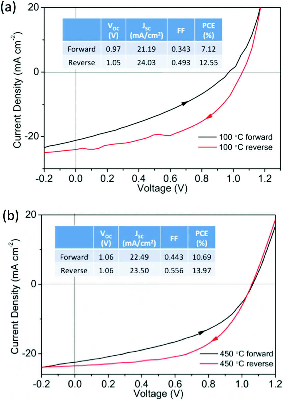 | ||
| Fig. 2 Representative J–V curves for perovskite devices using (a) ZnO (100 °C) and (b) ZnO (450 °C) as ETLs, insets summarize performance characteristics. | ||
In an attempt to improve thermal stability and reduce J–V hysteresis a modification of the interface between perovskite and ZnO was investigated. PCBM was chosen as the modifier, as it is commonly implemented as an ETL in perovskite devices.31To align with our objective of preparing devices at low temperature the modification was conducted on ZnO treated at 100 °C. The XRD patterns obtained for modified and non-modified ZnO after annealing at 100 °C in N2 for 20 min are shown in Fig. 3a. The presence of a strong PbI2 diffraction peak for the unmodified film is notably absent for the ZnO modified with PCBM, indicating improved thermal stability in the modified ZnO system. The PCBM modification was also shown to significantly reduce the J–V hysteresis, Fig. 3b. Improved performance characteristics were achieved with ZnO/PCBM bilayer as ETLs, with negligible J–V hysteresis at a 0.2 V s−1 scan rate (forward and reverse bias) and measured values of: PCE (15.1%); VOC (1.0 V); JSC (20.5 mA cm−2) and a FF of 0.74. Thus, a low-temperature processed (<100 °C), thermally stable, and efficient perovskite solar cells with a conventional architecture showing negligible hysteresis can be obtained using the modified ZnO ETL with an interfacial layer of PCBM.
 | ||
| Fig. 3 (a) XRD patterns of glass/ITO/ZnO/CH3NH3PbI3 and glass/ITO/ZnO/PCBM/CH3NH3PbI3, both annealed at 100 °C in N2 atmosphere for 20 min, showing PCBM can dramatically increase the upper perovskite stability; (b) representative J–V curves for perovskite devices using ZnO (100 °C)/PCBM bilayer as electron transport layer, indicating good performance with negligible hysteresis. | ||
The addition of PCBM led to a small loss of JSC, 20.5 mA cm−2 (ZnO/PCBM) compared to 24.0 mA cm−2 (ZnO only). This may be caused by increased light absorption from PCBM, confirmed from UV-visible transmission spectra in Fig. 4a, thus fewer absorbed photons result in subtle reductions in measured JSC. Similarly the measured VOC falls from 1.05 V in the unmodified ZnO device to 1.0 V with the PCBM modified ETL. In the unmodified case we believe that some of the decomposition product i.e. PbI2 present in the grain boundaries may reduce grain boundary recombination thus subtly improve VOC.32,33 However in addition to stability enhancements overall the PCE improves, owing to a substantial improvement in FF upon surface modification. To investigate the enhancement in FF the surface morphology of as-prepared and surface modified ZnO films were analysed by atomic force microscopy (AFM), Fig. 4b. There is a significant reduction in RMS roughness from the unmodified ZnO (3.2 nm) to the PCBM modified surface (0.3 nm) that improves interfacial contact between the ETL and perovskite thus improving FF. Of course, another important reason for negligible hysteresis current curve with PCBM is that the fullerene passivates the charge trap states on perovskite surfaces, which has been proved on both inverted31 and conventional34–36 perovskite device structures. Finally the PCBM also modifies the Fermi level (EF) of the oxide ETL, Fig. 5, which in the modified system decreases by around 0.1 eV compared with the neat ZnO. A schematic energy level diagram of the device layers is shown in Fig. 5.8,37 The EF modulation improves energy level alignment which will enhance charge collection, may contribute to reduced J–V hysteresis37 and also to the improved FF. It is not possible to deconvolute the individual contributions to the FF by each of the mechanisms discussed here but is it plausible that each has a role to play in the performance enhancement.
 | ||
| Fig. 4 (a) UV-vis transmittance of glass/ITO/ZnO (100 °C) and glass/ITO/ZnO (100 °C)/PCBM stacks, indicating both high transmission in visible region, some additional absorption is seen on the addition of PCBM; (b) AFM images measured for the same stacks, revealing smoother ETL surface with PCBM modification. | ||
 | ||
| Fig. 5 Flat band energy level diagram showing the energy levels of the various materials contained in the devices measured. The change in work function of the ETLs is highlighted. | ||
Conclusions
We have investigated the incorporation of ZnO as an electron transport layer in perovskite photovoltaics. Our ZnO deposition route is remarkably simple, water-based thus environmentally friendly and results in operational devices that suffer from poor thermal stability and the presence of excessive current–voltage hysteresis. Additionally we discover that the processing temperature of the ZnO impacts both the composition and microstructure of the ZnO but also the microstructure of the perovskite active layer. To overcome the issues of current–voltage hysteresis we have investigated the incorporation of the thin layer of PCBM onto our ZnO to act as a stabilizer and interface modifier, which overcomes the issue of hysteresis and also induces thermal stability to the perovskite active layer.Experimental section
Fabrication
Indium tin oxide substrates (ITO, PsiOteC UK Ltd; 12–16 Ω sq−1) were cleaned using ultrasonics and sequential washing in acetone, isopropanol and distilled water prior to being dried with compressed nitrogen gas followed by a 10 minute UV-ozone clean (UVOCS).Carbon-free aqueous zinc solutions were prepared by mixing zinc oxide powders (Sigma Aldrich) in ammonium hydroxide solution (5.0 M, Sigma Aldrich) as solvent to molar concentration of 0.1 M. Before spin coating, the solutions were filtered through a 0.45 μm filter. The spin coating of ZnO films was a 2000 rpm spinning for 30 s with an acceleration rate of 1000 rpm s−1. Four coatings were applied to achieve a compact layer. The films were preheated at a given temperature for 10 min on a hotplate after each coating. Post annealing (Carbolite 5 L RWF) was conducted at the same given temperature for 1 hour under flowing air. PCBM was dissolved in chlorobenzene and heated at 60 °C while stirring overnight in a N2 filled glovebox. Spin coating was carried out in a glovebox at 1000 rpm for 30 s and then annealed at 70 °C for 3 min.
The MAPI precursor prepared by co-dissolving 1.25 M lead iodide and methylammonium iodide in mixed solvent of gamma-butyrolactone and dimethyl sulfoxide (7:3 by volume). The solution was stirred for 2 hours and was filtered before use. The perovskite active layer was formed via a “toluene-dripping” method reported by Jeon et al.26 The precursor solution was first spun at 500 rpm for 5 seconds and then 2000 rpm for 20 seconds. 50 ml of toluene was instantly dripped onto the film right at the end of second stage of spinning, and followed by spun at 4000 rpm for 20 seconds. The films were transferred onto a hotplate after spin coating, and were dried at 100 °C for 20 seconds to crystalize the perovskite. Finally the devices were annealed at 100 °C on a hotplate for 10 minutes. Both the spin coating and annealing process were carried out in a N2 filled glovebox.
The hole transport material was prepared by dissolving 82 mg 2,2′,7,7′-tetrakis[N,N-di(4-methoxyphenyl)amino]-9,9′-spirobifluorene (spiro-OMeTAD) in 1 ml chlorobenzene. 15.6 μL of bis(trifluoromethane)sulfonimide lithium salt (Li-TFSI) solution (450 mg in 1 mL of acenitride) and 24.4 μL of 4-tert-butylpyridine were added to the pristine solution as additives. The solution was stirred for 30 minutes and was filtered before use. Hole transportation layer was formed by spun the solution onto perovskite film at 3500 rpm for 45 s. The devices were stored in dry ambient condition for 24 hours to allow the oxidation of Spiro-OMeTAD.
Finally, the deposition of the top electrode is carried out in a nitrogen filled glovebox evaporator, with a shadow mask used to spatially define the electrode (4.5 mm2). The top electrode is composed of 10 nm of MoO3 and 100 nm of Ag; the evaporation rate of MoO3 was 0.1–0.2 nm s−1 and that of Ag was 0.8–1.0 nm s−1.
Characterization
Film thicknesses were measured using a surface profilometer (Dektak 150). Optical transmission of ITO was measured using a custom single-beam UV-vis spectrometer. Film morphology was assessed using (i) a LEO Gemini 1525 Field Emission Scanning Electron Microscope (FESEM) with the addition of a 5 nm layer of chromium, and (ii) a Bruker Multimode Nanoscope AFM with image processing carried out using the Gwyddion software suite. XRD measurements were carried out using a Panalytical X'Pert Pro diffractometer (CuKα). Work functions were calculated from the measured chemical potential using a Kelvin probe (SKP5050 by KPTechnology) in air, calibrated to a highly ordered pyrolytic graphite reference (work function = 4.47 eV).38 Contact angles of perovskite precursor solution droplets on ZnO film surfaces were measured using an optical microscope (Veho Discovery VMS-004). Data analysis was conducted using Image J to accurately fit droplet radius and measure contact angle between drop and substrate.Device testing
Perovskite solar cells J–V characteristics were measured using a xenon lamp (1 Sun, AM 1.5 G) (Oriel Instruments) with a Keithley 2400 source meter. The intensity was adjusted to 1 sun by changing the working current, which was calibrated using a Si reference photodiode. All devices were stored in dark prior to measurement and were measured in a nitrogen-filled chamber.Conflicts of interest
There are no conflicts of interests to declare.Acknowledgements
JZ and MM would like to thank the China Scholarship Council for funding support. Additionally we acknowledge the EPSRC Centre for Doctoral Training in Plastic Electronic Materials EP/L016702/1 for student support and training and the EPSRC-Imperial College International Student Scholarship for financial support.Notes and references
- M. A. Green, K. Emery, Y. Hishikawa, W. Warta and E. D. Dunlop, Prog. Photovolt: Res. Appl., 2016, 24, 905–913 CrossRef.
- W. S. Yang, J. H. Noh, N. J. Jeon, Y. C. Kim, S. Ryu, J. Seo and S. Il Seok, Science, 2015, 348, 1234 CrossRef CAS PubMed.
- Q. Dong, Y. Fang, Y. Shao, P. Mulligan, J. Qiu, L. Cao and J. Huang, Science, 2015, 347, 967–970 CrossRef CAS PubMed.
- S. D. Stranks, G. E. Eperon, G. Grancini, C. Menelaou, M. J. P. Alcocer, T. Leijtens, L. M. Herz, A. Petrozza and H. J. Snaith, Science, 2013, 342, 341–344 CrossRef CAS PubMed.
- S. D. Stranks and H. J. Snaith, Nat. Nanotechnol., 2015, 10, 391–402 CrossRef CAS PubMed.
- B. O'Regan and M. Grätzel, Nature, 1991, 353, 737–740 CrossRef.
- M. M. Lee, J. Teuscher, T. Miyasaka, T. N. Murakami and H. J. Snaith, Science, 2012, 338, 643–647 CrossRef CAS PubMed.
- H. Zhou, Q. Chen, G. Li, S. Luo, T. B. Song, H. S. Duan, Z. Hong, J. You, Y. Liu and Y. Yang, Science, 2014, 345, 542–546 CrossRef CAS PubMed.
- D. Liu and T. L. Kelly, Nat. Photonics, 2013, 8, 133–138 CrossRef.
- D. Y. Liu and T. L. Kelly, Nat. Photonics, 2014, 8, 133–138 CrossRef CAS.
- E. A. Meulenkamp, J. Phys. Chem. B, 1998, 102, 5566–5572 CrossRef CAS.
- I. Litzov and C. Brabec, Materials, 2013, 6, 5796–5820 CrossRef PubMed.
- S. T. Meyers, J. T. Anderson, C. M. Hung, J. Thompson, J. F. Wager and D. A. Keszler, J. Am. Chem. Soc., 2008, 130, 17603–17609 CrossRef CAS PubMed.
- Y. H. Lin, H. Faber, K. Zhao, Q. Wang, A. Amassian, M. A. McLachlan and T. D. Anthopoulos, Adv. Mater., 2013, 25, 4340–4346 CrossRef CAS PubMed.
- S. Y. Park, B. J. Kim, K. Kim, M. S. Kang, K. H. Lim, T. Il Lee, J. M. Myoung, H. K. Baik, J. H. Cho and Y. S. Kim, Adv. Mater., 2012, 24, 834–838 CrossRef CAS PubMed.
- H. Faber, S. Das, Y.-H. Lin, N. Pliatsikas, K. Zhao, T. Kehagias, G. Dimitrakopulos, A. Amassian, P. A. Patsalas and T. D. Anthopoulos, Sci. Adv., 2017, 3, e1602640 CrossRef PubMed.
- Y. H. Lin, H. Faber, J. G. Labram, E. Stratakis, L. Sygellou, E. Kymakis, N. A. Hastas, R. Li, K. Zhao, A. Amassian, N. D. Treat, M. McLachlan and T. D. Anthopoulos, Adv. Sci., 2015, 2, 1–12 Search PubMed.
- S. R. Thomas, P. Pattanasattayavong and T. D. Anthopoulos, Chem. Soc. Rev., 2013, 42, 6910 RSC.
- Y. Peng, N. Yaacobi-Gross, A. K. Perumal, H. A. Faber, G. Vourlias, P. A. Patsalas, D. D. C. Bradley, Z. He and T. D. Anthopoulos, Appl. Phys. Lett., 2015, 106, 243302 CrossRef.
- J. Zhou, X. Meng, X. Zhang, X. Tao, Z. Zhang, J. Hu, C. Wang, Y. Li and S. Yang, Mater. Chem. Front., 2017, 131, 6050–6051 Search PubMed.
- R. M. Hewlett and M. A. McLachlan, Adv. Mater., 2016, 28, 3893–3921 CrossRef CAS PubMed.
- J. Yang, B. D. Siempelkamp, E. Mosconi, F. De Angelis and T. L. Kelly, Chem. Mater., 2015, 27, 4229–4236 CrossRef CAS.
- T. Oku, Crystal Structures and Related Perovskite Compounds Used for Solar Cells, 2015 Search PubMed.
- N. Onoda-Yamamuro, O. Yamamuro, T. Matsuo and H. Suga, J. Phys. Chem. Solids, 1992, 53, 277–281 CrossRef CAS.
- C. Bi, Q. Wang, Y. Shao, Y. Yuan, Z. Xiao and J. Huang, Nat. Commun., 2015, 6, 7747 CrossRef CAS PubMed.
- N. J. Jeon, J. H. Noh, Y. C. Kim, W. S. Yang, S. Ryu and S. Il Seok, Nat. Mater., 2014, 13, 1–7 Search PubMed.
- Y. Zhang, M. Liu, G. E. Eperon, T. C. Leijtens, D. McMeekin, M. Saliba, W. Zhang, M. de Bastiani, A. Petrozza, L. M. Herz, M. B. Johnston, H. Lin and H. J. Snaith, Mater. Horiz., 2015, 2, 315–322 RSC.
- B. Wu, K. Fu, N. Yantara, G. Xing, S. Sun, T. C. Sum and N. Mathews, Adv. Energy Mater., 2015, 5, 1500829 CrossRef.
- J. Zhang, J. C. D. Faria, M. Morbidoni, Y. Porte, C. H. Burgess, K. Harrabi and M. A. McLachlan, Adv. Electron. Mater., 2016, 2, 1600008 CrossRef.
- Y. Shao, Y. Fang, T. Li, Q. Wang, Q. Dong, Y. Deng, Y. Yuan, H. Wei, M. Wang, A. Gruverman, J. Shield and J. Huang, Energy Environ. Sci., 2016, 501, 395–398 Search PubMed.
- Y. Shao, Z. Xiao, C. Bi, Y. Yuan and J. Huang, Nat. Commun., 2014, 5, 1–7 Search PubMed.
- Q. Chen, H. Zhou, T. Bin Song, S. Luo, Z. Hong, H. S. Duan, L. Dou, Y. Liu and Y. Yang, Nano Lett., 2014, 14, 4158–4163 CrossRef CAS PubMed.
- T. Du, C. Burgess, J. Kim, J. Durrant, J. Zhang and M. McLachlan, Sustainable Energy Fuels, 2017, 1, 119–126 CAS.
- Y. Hou, C. O. R. Quiroz, S. Scheiner, W. Chen, T. Stubhan, A. Hirsch, M. Halik and C. J. Brabec, Adv. Energy Mater., 2015, 5, 1501056 CrossRef.
- A. H. Ip, L. N. Quan, M. M. Adachi, J. J. McDowell, J. Xu, D. H. Kim and E. H. Sargent, Appl. Phys. Lett., 2015, 106, 143902 CrossRef.
- C. Tao, S. Neutzner, L. Colella, S. Marras, A. Ram, S. Kandada, M. Gandini, M. De Bastiani, G. Pace, L. Manna, M. Caironi, C. Bertarelli and A. Petrozza, Energy Environ. Sci., 2015, 8, 2365–2370 CAS.
- L. Zuo, Z. Gu, T. Ye, W. Fu, G. Wu, H. Li and H. Chen, J. Am. Chem. Soc., 2015, 137, 2674–2679 CrossRef CAS PubMed.
- W. N. Hansen and G. J. Hansen, Surf. Sci., 2001, 481, 172–184 CrossRef CAS.
Footnote |
| † Electronic supplementary information (ESI) available: Contact angle, SEM image of MAPI on PCBM. See DOI: 10.1039/c7qi00667e |
| This journal is © the Partner Organisations 2018 |