
 Open Access Article
 This Open Access Article is licensed under a
 Creative Commons Attribution 3.0 Unported Licence
Silver nanowires for highly reproducible cantilever based AFM-TERS microscopy: towards a universal TERS probe†
Peter
Walke
a,
Yasuhiko
Fujita
 *ab,
Wannes
Peeters
a,
Shuichi
Toyouchi
a,
Wout
Frederickx
a,
Steven
De Feyter
a and
Hiroshi
Uji-i
*ac
*ab,
Wannes
Peeters
a,
Shuichi
Toyouchi
a,
Wout
Frederickx
a,
Steven
De Feyter
a and
Hiroshi
Uji-i
*ac
aDepartment of Chemistry, KU Leuven, Celestijnenlaan 200F, Heverlee, B-3001, Belgium. E-mail: yasuhiko_fujita@trc.toray.co.jp; hiroshi.ujii@kuleuven.be
bToray Research Center, Inc., 3-3-7, Sonoyama, Otsu, Shiga 520-8567, Japan
cRIES, Hokkaido University, N20 W10, Kita-Ward Sapporo 001-0020, Japan
First published on 29th March 2018
Abstract
Tip-enhanced Raman scattering (TERS) microscopy is a unique analytical tool to provide complementary chemical and topographic information of surfaces with nanometric resolution. However, difficulties in reliably producing the necessary metallized scanning probe tips has limited its widespread utilisation, particularly in the case of cantilever-based atomic force microscopy. Attempts to alleviate tip related issues using colloidal or bottom-up engineered tips have so far not reported consistent probes for both Raman and topographic imaging. Here we demonstrate the reproducible fabrication of cantilever-based high-performance TERS probes for both topographic and Raman measurements, based on an approach that utilises noble metal nanowires as the active TERS probe. The tips show 10 times higher TERS contrasts than the most typically used electrochemically-etched tips, and show a reproducibility for TERS greater than 90%, far greater than found with standard methods. We show that TERS can be performed in tapping as well as contact AFM mode, with optical resolutions around or below 15 nm, and with a maximum resolution achieved in tapping-mode of 6 nm. Our work illustrates that superior TERS probes can be produced in a fast and cost-effective manner using simple wet-chemistry methods, leading to reliable and reproducible high-resolution and high-sensitivity TERS, and thus renders the technique applicable for a broad community.
Introduction
Modern analytical tools such as Tip-enhanced Raman Scattering1 (TERS) or Tip-enhanced Fluorescence2 (TEF), are becoming increasingly invaluable to elucidate properties of arbitrary surface analytes with nanoscale precision. By coupling the family of scanning probe microscopies (SPM) with laser spectroscopy, via the introduction of a nanostructured metallic tip, detailed chemical maps can be formed at resolutions far beyond the diffraction limit of light. The tip acts in effect as an optical antenna;3 upon irradiation with incident light, surface plasmons excited close to the apex serve to generate a near-field that greatly enhances signals generated from the vicinity of the antenna apex. The tip or sample can then be raster-scanned to produce complementary nanoscale optical and topographic images. Correlation of these images allows for unique insight into nanoscale structure–property relationships. The optical resolution ranges from sub-nanometer to several tens of nanometers, dependent on the sample, scanning conditions, SPM architecture and the particular properties of the tip. Besides its superior resolution, TERS is a highly sensitive, non-invasive and label-free technique, with potential applications across a range of fields in the biological4,5 and physical sciences.6–8Following the development of scanning tunnelling microscopy (STM) by Binnig and Rohrer in 1982,9 several types of SPM design have been employed for surface analysis. Amongst these, cantilever-based atomic force microscopy (AFM) has several advantages. Cantilever-based AFM has, unlike STM, no intrinsic substrate limitations. It is also the most stable and fastest of all SPM imaging modes. During measurements the tip is usually either in hard-contact or oscillating dynamically close to the surface. When a dynamic-mode feedback mechanism (or ‘tapping-mode’) is employed, surface imaging and force analysis on soft materials such as polymers or bio-specimens becomes routine. Here, the cantilever is driven close to resonance and the tip–sample separation is modulated to maintain a specific oscillation amplitude or frequency. Indeed, using dynamic feedback modes has allowed for topographic imaging,10 manipulation11 and identification12 with atomic resolution. The performance and versatility of cantilever-based AFM in tapping-mode makes it by far the most commonly implemented SPM mode in modern research. But in the field of TERS, efficient production of the tips required for cantilever-based AFM-TERS microscopy remains under-developed: resolution and performance lag behind STM-TERS microscopy,13 where the most notable TERS results have so far been reported.14–17
In general, tips for cantilever-based AFM-TERS are prepared via vacuum deposition of a thin layer of gold or silver onto a standard silicon-based AFM cantilever.18,19 But such tips commonly suffer from a combination of both low-reproducibility20 and short-lifetime,21 allied to the requirement for technical and specialised fabrication protocols and an associated prohibitively high cost. The Raman enhancement and plasmon dipole orientation are not consistent even within the same batch of tips, vastly complicating the acquisition of results and their subsequent analysis.22 It is also usual for the probes to provide a lesser Raman enhancement than the electrochemically etched gold/silver tips used for STM-TERS microscopy.13 This is especially the case when operating AFM in tapping-mode due to the comparatively larger average tip–sample distance. The relative lack of enhancement is compensated for by operating the AFM in contact-mode, which is now used as standard, but this tends to limit probe lifetime due to the weakness of the metallic adlayer,21 in addition to being sub-optimal for certain samples. When tapping-mode has been used it has typically produced only very weak signals, meaning that very few tapping-mode AFM-TERS studies have been reported. This is especially true when applied to high resolution mapping,23 with lock-in detection24 typically required to obtain results.
In this context, novel methods for the reliable fabrication of TERS probes are actively being pursued.25 This includes the proof of concept attachment of polycrystalline silver nanowires to AFM cantilevers for TERS by Brodard et al.26 using electron microscopy and a micromanipulator. Though some progress has been made through so called ‘top-down’ approaches,27 precise control of metal nanostructure composition is still difficult and improvements to tip lifetime are not expected. These also still require highly expensive and specialised equipment out of reach to most researchers, including the stated use of electron microscopy that is liable to induce amorphous carbon contamination. This is something that has been a typical issue for TERS.28,29 Attention has as a result shifted towards tips based around colloidal noble metal nanoparticles,30–32 the synthesis of which falls within the domain of ‘bottom-up’ nano-engineering. The shape, size and composition of such particles can be readily controlled with high homogeneity and on a large scale, making them ideal for plasmonic applications.33 Additionally, they help to limit tip-degradation34,35 as they exhibit superior mechanical properties compared to the corresponding bulk material. For example, the Young's modulus of silver nanowires can reach up to 160 GPa,36 around 3 times greater than found in bulk.
However, no fast and scalable fabrication method for colloidal based TERS probes has demonstrated sufficiently high performance in terms of both topographic and Raman imaging. Resolution and reproducibility are still lacking, and application to tapping-mode TERS has yet to be realised. This makes the development of a high-performance and cost-effective probe still the critical issue in TERS.
Here we propose a new AFM-TERS tip based on the functionalisation of standard AFM cantilevers with chemically-synthesised silver nanowire (AgNW) assemblies. We demonstrate TERS imaging far below the diffraction limit in both tapping and contact feedback modes. The tips are also shown to provide excellent topographic scanning on a variety of nanostructured samples. Owing to the well-controlled apex structure and excellent optical coupling afforded by the synthesis, the fabricated tips show a TERS reproducibility greater than 90%, when tested in contact-mode, as well as Raman signals enhanced by a factor of 10 over the gold tips most commonly used for STM-/shear-force AFM-TERS microscopy. Representative enhancement factors are estimated as about 106. The tips typically achieved a resolution of around 15 nm when used to image single-walled carbon nanotubes (CNTs) on a gold substrate under contact mode. Moreover, thanks to the high enhancement achieved, Raman signals can still be obtained in tapping-mode without lock-in detection, for which the highest obtained resolution was below 6 nm. The results described herein show that high performance AFM-TERS tips can be generated practically and at low-cost using simple wet-chemical methods, and will serve to greatly accelerate the proliferation of TERS as a unique tool for nanoscale analysis.
Experimental
Materials
Isopropanol (IPA), polyvinylpyrrolidone (PVP), ethylene glycol (EG), silver nitrade (AgNO3), copper chloride (CuCl2), cysteamine, hydrochloric acid (HCl), poly-L-lysine (PLL) were obtained from Sigma Aldrich. H12SC6O-azobenzene was obtained from Prochimia. All chemicals were used without further purification.Silver nanowire synthesis
The nanowires were fabricated using the polyol method, as described elsewhere.37 Briefly, after heating up 5 mL of 0.15 M PVP solution in EG at 150 °C for 15 min, 40 μL of CuCl2 (4 × 10⁻³ M) solution in EG was injected, followed by adding 2.5 mL of AgNO3, while the EG solution was added in a drop-wise manner under magnetic stirring (600 rpm). Then the solution was kept at 150 °C for another 1.5 h, obtaining high-yield silver nanowires. These nanowires were then washed three times with ethanol. Thereafter, the PVP surfactant was replaced by stirring 0.1 mL of the as synthesised nanowire solution into 0.9 mL of a 0.5 mM solution of cysteamine in iso-propanol (IPA) for 24 h (stirring rate 600 rpm). Finally, the nanowires were washed 3 times in IPA. Average diameter and length of the silver nanowires were 120 nm and 10 μm, respectively.Fabrication of silver nanowire functionalised AFM tip
Tip-view type AFM cantilevers (ACCESS-NC-A, AppNano) were dipped into a silver nanowire solution deposited on a cleaned ITO or FTO substrate with which the solution was supported by an elastomer (polydimethylsiloxane, PDMS) containing a central hole. The solution typically contains approximately 10–20 μL of 10–40 times diluted silver nanowire solution with a few drops (∼50 μL) of Milli-Q water. The cantilever was submerged into the solution whilst being monitored by a charge-coupled device (CCD) camera. Then a square voltage of 2–12 Vp–p (duty 50%, 1–2 MHz) provided by a function generator (4052, BK Precision) was applied for usually 1–10 s between the cantilever and the conductive plate to achieve the nanowire attachment. Finally, the length/angle of the nanowires attached to the cantilever apex was checked in situ or with high magnification optical microscope.Fabrication of etched Au tips
The gold tips were fabricated by electrochemical etching of a gold wire using a concentrated HCl solution.38 The gold wire (MaTecK, φ 0.25 mm) was partially dipped in a 1![[thin space (1/6-em)]](https://www.rsc.org/images/entities/char_2009.gif) :1 mixture of IPA and fuming HCl and a DC 2.4 V was applied between the gold wire and a counter electrode (ring-shaped gold wire, φ 0.5 mm). Finally, the tips were washed in IPA/H2O several times.
:1 mixture of IPA and fuming HCl and a DC 2.4 V was applied between the gold wire and a counter electrode (ring-shaped gold wire, φ 0.5 mm). Finally, the tips were washed in IPA/H2O several times.
Preparation of monolayer azobenzene-thiol on Au(111)
Au(111) substrates purchased from Arrandee were first flame annealed with an O2 burner for around 60 s and then cooled with N2 atmosphere for 5 min to remove contamination. The substrates were then deposited in a ∼2 mM solution of HS-C6H12-O-azobenzene (Prochimia) in Isopropanol for approximately 12 h. Note that the solution was de-gassed with Argon prior to use. Finally, the substrates were removed from the solution and were washed with IPA several times to completely remove unbound thiol molecules.Preparation of DNA on mica
Prior to DNA deposition, mica was functionalised with poly-L-lysine (PLL) by incubating 20 μl of a 0.01% w/v PLL (MW 500–2000, Sigma Aldrich) solution for 30 seconds on freshly cleaved mica. The sample was then gently rinsed with 50 mL Milli-Q water and dried with a gentle flow of Argon gas. DNA molecules of approximately 500 bp were diluted to a final concentration of ∼0.5 ng μL−1 in a buffer containing 200 mM Na-acetate and 10 mM Tris-HCl (pH = 7.6). A 10 μL-solution was deposited onto the poly-L-lysine-coated mica for 30 seconds before the sample was again gently rinsed with 20 mL Milli-Q water and finally dried using a gentle flow of Argon gas.AFM/TERS measurements
AFM/TERS measurements were performed on an Omegascope™ (AIST-NT) with a home-made optical platform. Laser light from a He–Ne laser (632.8 nm) was reflected by a dichroic mirror (Chroma, Z633RDC) and then focussed onto the sample/tip by an objective (MITUTOYO, BD plan Apo 100×, N.A. 0.7). Raman scattering was collected using the same objective and directed to a CCD camera (Andor, Newton 920) equipped on a Raman spectrograph (Horiba JY, iHR-320) through the dichroic mirror, a pinhole and a long pass filter (Chroma, HQ645LP). Polarization of incident light was set to maximise the TERS contrast/resolution (often parallel to the nanowire long axis). A stage was designed in house to hold the SPM unit at an angle of 60° (side-illumination) or 0° (top-illumination) to the optical axis. Laser alignment to the tip apex was done by recording Rayleigh scattering mapping as the objective was scanned in the XY/XZ plane under fixed tip position. Measurements were carried out under ambient conditions and at room temperature. All AFM/Raman measurements were processed using Gwyddion/IGOR Pro software.Enhancement factor calculations
The median far-field signal was used in all cases to account for sample variations, with only positions where a clear peak could be seen taken into account. In many cases there was no far-field signal and hence the value stated for the contrast can be seen as a lower bound for both the etched gold and AgNW tips.Results and discussion
Tip fabrication & characterization
The tips were fabricated using the alternating-current dielectrophoresis (AC-DEP) method. This method allows nanoparticles in a medium to be manipulated by a non-uniform electric field. The strength of the applied force is proportional to the gradient of the magnitude of the applied electric field.39 The procedure is similar to methods previously described for STM-TERS microscopy40 and live-cell endoscopy,41 but was modified based on the low intrinsic conductivity of the cantilevers and the desire to limit the length of the assemblies. The choice of nanowires was made due to their quasi-1D dimensions and micrometre length, and the fact that the size and composition of the nanowires can be readily adapted dependent on sample and system requirements.42,43Fig. 1a shows a schematic of the system used for attachment. A solution containing chemically-synthesised silver nanowires (diameter ∼120 nm (ref. 37)) was deposited onto a conductive substrate (Tin-doped Indium Oxide, ITO, or fluorine-doped tin oxide, FTO), with the apex of a commercial AFM cantilever then dipped into this solution. Both the cantilever and substrate were electrically contacted to a pulsed voltage supply. The AgNW concentration was usually kept at or below 109 AgNW per L. Thereafter, a pulsed voltage between 2 and 12 V was applied for several seconds, before the cantilever was vertically retracted from the solution. The alignment of the AFM tip cone perpendicular to the solution surface means that the nanowires are preferentially attached in the direction of the tip. Fig. 1c–e show optical images taken before (c), during (d) and after (e) nanowire attachment to the AFM cantilever. | ||
| Fig. 1 (a) Schematic of tip attachment procedure. (b) Typical SEM image of an AFM tip after silver nanowire functionalisation (4 V, 3 s). (c–e) Optical transmission images during silver nanowire attachment to an AFM cantilever: before (c), during (d) and after (e) submersion into the silver nanowire solution. | ||
The functionalised probes were evaluated by either checking the optical image directly or by looking at the meniscus formed when the newly formed assembly is dipped slowly back into the solution. The length of the assembled AgNWs can then be estimated by the distance between the cantilever and the meniscus. This is especially convenient when looking at thin nanowires beneath the diffraction limit. In addition, the AgNWs can be detached in situ by simple submersion of the cantilever deep into the solution without applying any voltage, something that allows long or otherwise unsuitable assemblies to be removed and cantilevers reused. Indeed, too long nanowires were found to be unstable for AFM feedback (ESI, Fig. S1†), and so the attachment process was repeated until a desired length (<10 μm) was achieved. A scanning electron microscope (SEM) image of a typical AgNW tip fabricated with 4 V for 3 s is given in Fig. 1b. Though it is not necessary for single nanowires to be attached, often only single or few nanowires were assembled on the tip using these parameters, typically ranging in length from a few to 10 μm. The method as described here was found to be general, and nanowires of varying dimensions and composition could be assembled in a facile manner.
High-resolution topographic mapping in tapping-mode
As a first step following fabrication, topographic imaging was demonstrated with the AgNW tips using tapping-mode AFM. Fig. 2a and b show AFM images of a Silicon trench structure (TGZ3, NT-MDT) generated with an AgNW and an unfunctionalised conical-shaped tip, respectively. The height and period of the trench were given as 520 nm and 3 μm. Comparing the cross-sectional plots, steeper edge structures were found with the AgNW tip compared to the normal (unfunctionalised) tip. This more accurate tracing of the structure is a direct result of the quasi-1D shape of the AgNWs themselves, and has similarly been found with other high-aspect ratio tips, such as those modified with carbon nanotubes.44 Furthermore, the AgNW probes could also be used to image graphite step-edges or single linear DNA molecules (Fig. 2c and d), illustrating sub-nanometre sensitivity in the Z-direction.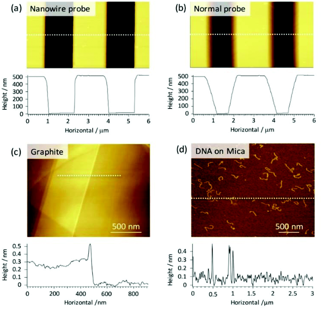 | ||
| Fig. 2 (a, b) AFM images and line profiles of a calibration grating using a silver nanowire (a) and an un-functionalised (b) tip. (c, d) AFM height images observed using a nanowire tip of freshly-cleaved graphite (c) and DNA on Mica (d), along with associated line profiles. All AFM images were obtained under tapping-mode AFM feedback with isolation of acoustic and vibrational noises. | ||
Information regarding the lateral resolution was also extracted from the results on DNA (Fig. S2c and d†). Measurements of the separation between 2 approximately parallel DNA molecules indicate that the true lateral resolution in tapping-mode was at least 25 nm with the nanowire tips, which compares well to the value of 21 nm similarly extracted using an unfunctionalised probe. The full-width at half maximum (FWHM) of a single DNA molecule also increased from around 12 nm using an unfunctionalised probe, to a value of 15 nm with an AgNW tip (Fig. S2e and f†).
These changes are likely a result of the expected increase in tip curvature for the nanowire probe. Nevertheless, the results validate that tip sensitivity in both the Z-direction and X, Y-plane is sufficient for AFM imaging, and indicates the applicability of the developed probes over a wide range of nanoscale systems.
Strength and reproducibility of the near-field Raman scattering
The primary use of the nanowire tips is as effective probes for TERS measurements and related techniques in near-field spectroscopic imaging. The strength and reproducibility of the TERS signal using the AgNW tips was therefore assessed against the electrochemically etched gold probes that are employed as standard in STM-/shear-force AFM-TERS microscopy.38 The reference tips were approached onto the surface using an STM feedback mechanism.The choice of 633 nm as the excitation source was made based on dark-field spectroscopy45 measurements of the tip Plasmon resonance for both the AgNW and etched Au tips. These spectra typically showed peaks at around 600 nm, as shown in Fig. S5.† Indeed, TERS measurements performed using AgNW tips on the same azo-benzene thiol substrate with two wavelengths (633 nm and 532 nm) indicated that the signal to noise ratio of the TERS signal was approximately 26× higher with 633 nm excitation than with 532 nm (Fig. S5†).
A sample of azobenzene-thiol chemisorbed on an Au(111) substrate was used for the measurements. Azobenzene thiols on gold are a commonly used system to evaluate aspects of TERS,46 due to the large Raman cross-section of the azobenzene moiety and the detailed spectra that can be obtained. The gold substrate allowed a highly-confined hybridized plasmonic mode (gap-mode) to be supported.47,48Fig. 3a shows typical spectra recorded with the AgNW tip both approached in contact-mode and in a retracted position from the surface. For the far-field measurement, when the tip was withdrawn from the surface, only the strongest band at approximately 1140 cm−1 can be discriminated above the noise level. Conversely, with the tip-engaged the characteristic bands of the azo-benzene moiety can be unambiguously identified, and clearly illustrates that the fabricated tips work as effective plasmonic antennas for near-field spectroscopic measurements.
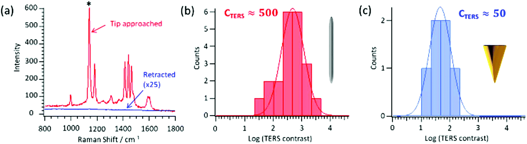 | ||
| Fig. 3 (a) Typical spectra of azobenzene-thiol on an Au(111) surface, recorded with the tip approached (red) and retracted (blue) from the surface, respectively. The spectra were recorded under contact-mode AFM feedback and with side-illumination configuration, with the light polarized approximately parallel to the tip long axis. (b, c) Histograms of the logarithmic TERS contrast for the silver nanowire (b) and etched Au (c) tips, along with fitted Gaussian profiles in each case. An STM feedback mechanism was used for the reference Au tips. The power was kept below 19 kW cm−2. | ||
Next, the tip-to-tip reproducibility was assessed. In total, it was found that over 90% of all nanowire tips that could be approached onto the surface could be used for TERS measurements (28 of 30 tested). A more quantitative basis for the performance of a respective probe can be made using the TERS contrast, CTERS, and/or enhancement factor, EF, given by the following two equations:
 | (1) |
 | (2) |
Fig. 3b and c provide histograms of the contrast for the AgNW and electrochemically-etched gold tips, respectively. As stated, in the far-field only the peak at 1140 cm−1, assigned to the stretching of the two CN moieties,51 ever gave a sufficient signal to be analysed, and so only the contrast of this particular mode was considered. To exclude any surface effects, a TERS contrast greater than 10 was set as judgement criterion. This was passed for all 21 of the silver nanowire tips used to test the TERS contrast, with 90% giving a value better than 80. Conversely, of the 9 measured Au tips, only 6 were found to yield a contrast greater than 10, and only a single tip gave a TERS contrast more than 100. From the fits the mean values of the logarithmic TERS contrast for the two tip types were correspondingly 2.7 ± 0.5 for the AgNW tip and 1.7 ± 0.5 for the etched gold, meaning that the AgNW tips thus gave a signal on average 1 order of magnitude greater than the etched gold tips used as reference. By then taking into account the resolution of the AgNW tips, which, as detailed below was on the order of 15 nm, EF could then be approximated. In doing so, a representative figure for the enhancement factor in contact-mode and under the outlined conditions was about 106. The fact that the tips yield such high signals and reproducibility for the comparatively low power used probably results from the strong optical coupling at the apex. This is important as the play-off between laser power, acquisition time and TERS contrast is crucial for collecting spectra whilst minimising damage to the tip and/or sample.
Benchmarking TERS resolution on carbon nanotubes in contact-mode
The AgNW probes were further used to demonstrate Raman mapping of carbon nanotubes (CNTs) dispersed on Au(111). Spectra were recorded in a side-illumination configuration and with contact-mode. Fig. 4a shows an AFM topographic image of a single walled CNT‡ taken with an AgNW probe, along with a zoomed image. Fig. 4b in turn displays several point spectra recorded at the positions indicated in Fig. 4a. Although each point is only separated by about 100 nm, heterogeneity on the CNT could be clearly discriminated. There was also no Raman signal observed on the bare gold substrate, despite this being only 50 nm from the CNT (point D), unambiguously illustrating that the resolution of the measurements is far beyond the diffraction limit.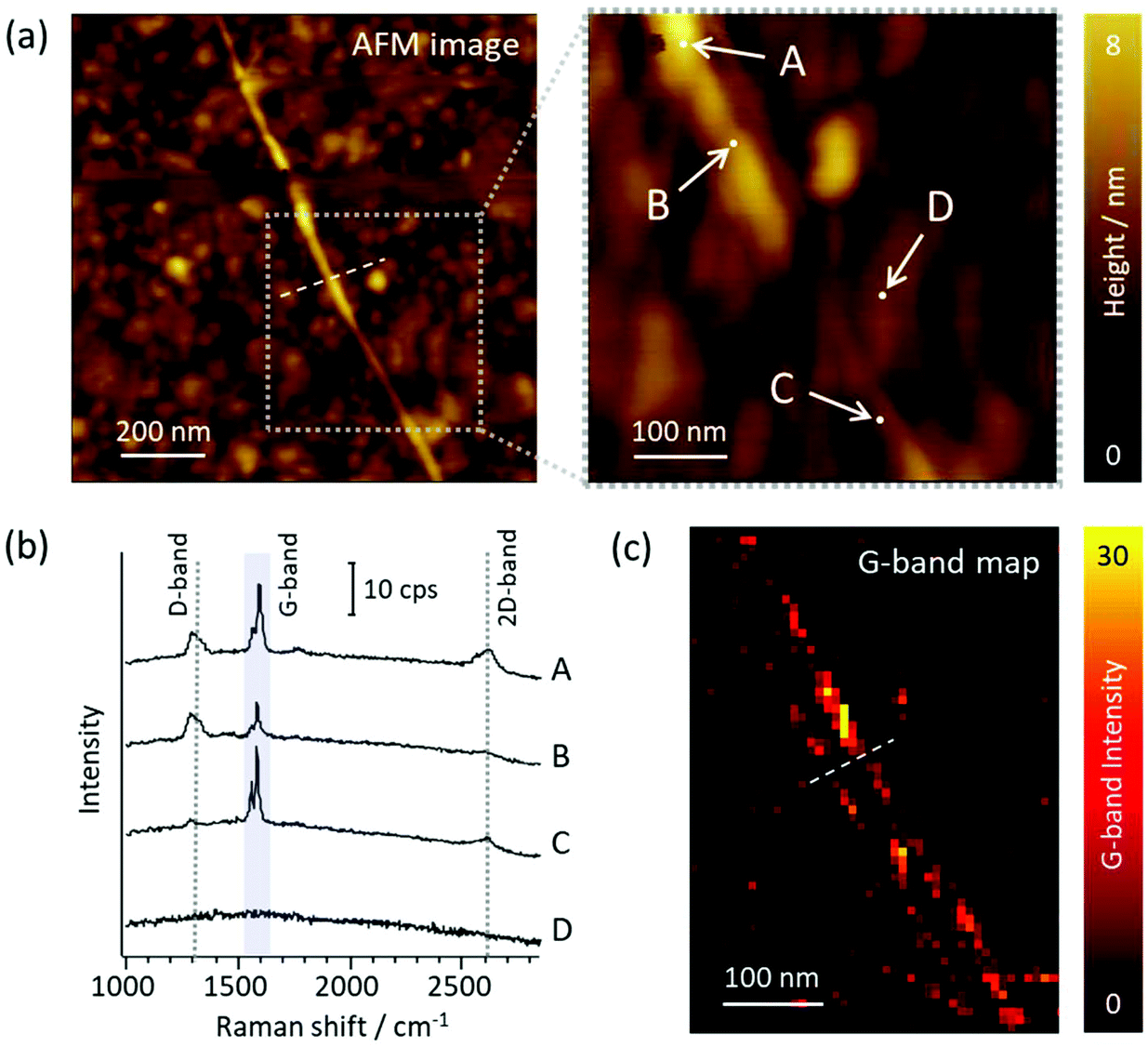 | ||
| Fig. 4 (a) Contact-mode AFM image of a CNT dispersed on Au(111) obtained with a silver nanowire-tip along with a zoomed image. (b) TERS spectra recorded at the positions indicated in (a). (c) Contact-mode TERS image displaying the G-band intensity of the same nanotube as found in (a). The pixel size was set to 8.3 nm. The spectrum at each pixel point was collected under irradiation of 632.8 nm laser light with approximately 28.0 kW cm−2 with an acquisition time of 0.3 s, and then the image was reconstructed by extracting G-band peak height after background subtraction. | ||
An image was thereafter recorded by raster scanning the sample beneath the tip and recording a full spectrum at each position (hyperspectral imaging). Fig. 4c shows the resultant image of the most prominent Raman feature, the G band, located for this CNT at around 1584 cm−1. Fig. 4c also shows a line profile across the nanotube, from which the resolution was estimated (Fig. S4b†) from the extracted FWHM of a Gaussian fitting. In the case shown it was found to be 18 nm which corresponds to an improvement by a factor of around 30 over that expected from far-field measurements. Note that as the CNT has finite width (and may additionally be bundled) this can be seen as an upper bound on the resolution. The topographic resolution similarly derived from the line profile in Fig. 4a gave a slightly greater value of ∼23 nm (Fig. S4a†), and further validates the concomitant nature of the optical and topographic resolutions.
Exceptional TERS resolution on carbon nanotubes in tapping-mode
Interestingly, it was found that TERS images could also be recorded in tapping-mode when high contrast tips were used. For these measurements the cantilever free oscillation amplitude was set to 20 nm. For mapping, a top-illumination configuration was chosen instead of side-illumination (Fig. S3†), to further increase the TERS sensitivity by suppressing the broad background arising from the far-field contribution.52Fig. 5a–c displays the intensity maps of the 3 most prominent Raman bands of CNTs;§ the defect induced D-band at ∼1300 cm−1, the G-band at ∼1590 cm−1, and the 2D band at around 2600 cm−1.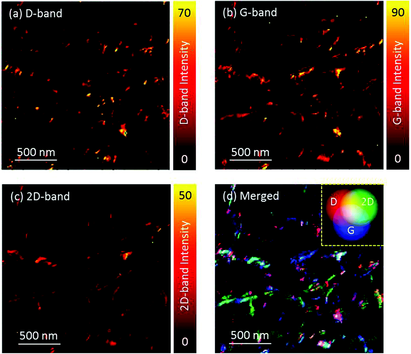 | ||
| Fig. 5 (a–c) TERS maps of D- (a), G- (b), and 2D-bands (c) of CNTs dispersed on Au(111) surface. The size of the maps was set to 2×2 μm with 150 pixel resolution (1 pixel = 13.3 nm). Spectrum at each pixel point was collected under irradiation of 632.8 nm laser light with approximately 43.0 kW cm−2 with an acquisition time of 0.3 s. Peak height after background subtraction was used for the map reconstruction. (d) Combined map of the D-, G- and 2D-bands. The red, blue, and green colours respectively correspond to D-, G-, and 2D-bands intensity. | ||
Fig. 5d presents the merged image of the 3 bands shown individually in the Fig. 5a–c. The positions and intensity ratios of the D-, G- and 2D-bands are intimately related to the physical nature of the CNTs, and to the characterisation of carbon materials more generally. For example, regions of the image exhibiting high D-band intensity allow for the localisation of defective regions on the CNTs. Broad D and G peaks at an intensity ratio close to unity, along with a greatly suppressed 2D band, are representative of graphene oxide or similar amorphous or graphitised carbon. Hence, this combined image vividly discriminates the heterogeneity of the sample to an extent not possible with traditional SPM, and indicates that defect sites or the degree of charge-carrier doping can be assessed at the single nanotube level.
Measurements of the resolution could also be carried out in tapping-mode using a higher resolution image, as shown in Fig. 6a. The same experimental conditions as Fig. 5 were employed for this image. Here, again, the G-band of the CNT was used, with Gaussian fittings of the extracted line profiles to determine the TERS resolution. Fig. 6b and c illustrate that the obtainable resolution was below 10 nm, and from one of the profiles even approached 6 nm – a value superior to that previously demonstrated for contact-mode. The interpretation of the two profiles is subtly different as Fig. 6c is representative of the ability to discriminate two closely spaced objects, and is therefore analogous to the Rayleigh criterion in normal optical microscopy. Resolutions were estimated for several tips and were found to be consistently at or below 15 nm.
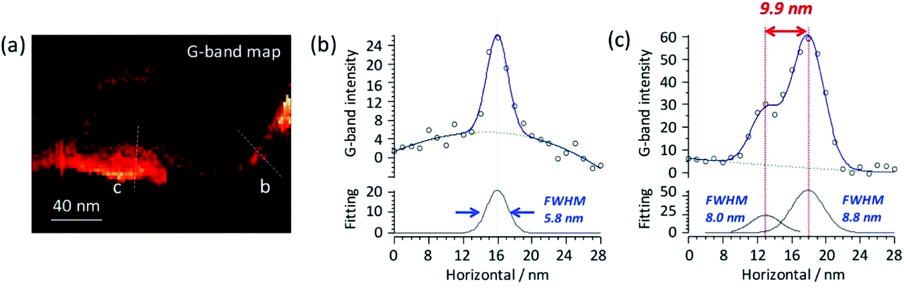 | ||
| Fig. 6 (a) TERS map of the G-band of CNT on Au(111) surface (acquisition time = 0.15 s). Pixel resolution was set to 2 nm. The same excitation conditions and analysis procedures as Fig. 5 were used. (b, c) Line profiles as designated in (a) along with fitted Gaussian profiles. | ||
It is typical for most modern AFM systems to utilise tapping-mode as default, as this is thought to provide more stable scanning at a higher resolution/speed than contact-mode, and it is possible that the results here could be reflective of this. The resolutions detailed are exceptionally high for an AFM based TERS system, particularly one which does not benefit from lock-in detection or any further processes to boost the signal sensitivity,53,54 and to the best of our knowledge we know of no cases of tapping-mode AFM-TERS measurements that have demonstrated the resolution and sensitivity detailed here.
Importantly, when measuring in tapping-mode the average force experienced by the tip is much weaker than found in contact-mode. Hard contact with the surface can induce morphological change in the tip apex and lead to a degradation in performance.21 Empirically in the field of TERS, tips are found to have scanning lifetimes that don't usually extend beyond a few hours of measurement at most, which may be mitigated by routine TERS operation in tapping-mode. This loss in tip performance over time may additionally arise from oxidation of silver – a typical problem in ambient surface-enhanced Raman scattering (SERS) experiments55 and a further understanding of these processes and their mitigation would be valuable.
Conclusions
Our work enlightens upon a simple, cost-effective and easily scalable method for producing nanowire-functionalised AFM tips, based on an alternating-current dielectrophoresis approach. Preparation of tips was found to be fast and cost-effective compared to other nanoparticle attachment methods such as the manipulator-based technique.26 The tips were tested on a variety of substrates for AFM and found to be capable of high-quality topographic imaging that in some cases even exceeded the performance of standard silicon probes. The tips were then shown to be effective for tip-enhanced Raman scattering (TERS) microscopy, yielding an average TERS contrast 1 order of magnitude greater than the electrochemically-etched gold probes used as standard for TERS measurements. The significantly improved signal enhancement was in conjunction with a TERS reproducibility greater than 90%. When used for Raman mapping of carbon nanotubes, optical resolution was found to be at least around 15 nm in contact-mode and, when used in tapping-mode, a maximum optical resolution of 6 nm could be obtained. This high performance owes to the excellent optical coupling as well as the good structural reproducibility of the chemically synthesized silver nanowires and distinguishes the approach used here from those based on so-called top-down methods.Though progress has been made using other bottom-up engineered optical antennas for TERS microscopy, none have successfully demonstrated the universal performance for both optical and topographic nano-imaging of the AgNW probes shown here. The quasi-1D structure of the nanowires is ideal for tip design, with minimal scope for dependence on orientation as might be expected for nanoparticles of other shapes, whilst the micrometre length is highly beneficial for assessing fabricated probes in situ. Additionally, mature fabrication protocols mean that nanowires of differing size and composition can easily be assembled on the cantilever, which is important given the assumption that TERS resolution and enhancement is largely dictated by tip dimension.
The aperture-less Near-Field optical microscopies, of which TERS is the most well-known, have long been expected to provide novel insights in a wide variety of fields, ranging from the mapping of active sites in heterogeneous catalysis, to descriptions of the nano-heterogeneity of novel materials and the local characterization of biologically relevant molecules. Such expectations have largely been stymied by the notorious difficulty in conducting experiments, a result of critical limitations in tip-production and, in this context, the introduction of such a method as described herein is a vital and necessary step. We therefore expect the work to greatly increase the scope of TERS by providing a means of moving the technique away from specialist research groups and into the domain of industry and the general scientific fields.
Conflicts of interest
There are no conflicts to declare.Acknowledgements
Authors thank Prof. D. Tanaka (Kwansei gakuin university, Japan) and P. Vernhout (AIST-NT Inc.) for providing samples of CNT on Au(111). Authors also thank Dr N. Naka, S. Kashiwagi, E. Iso, and Y. Okuno from Horiba Inc. (Japan) for providing test samples of Azobenzene on Au(111). This work was supported by JST PRESTO program, the Fund of Scientific Research-Flanders (FWO), Hercules Foundation, KU Leuven Internal Funds, Belgian Federal Science Policy Office (IAP-7/05), and the European Research Council under the European Union's Seventh Framework Programme (FP7/2007–2013)/ERC Grant Agreement No. 340324 to SDF and 280064 to HU. JSPS KAKENHI (JP17H03003, JP17H05244, JP17H05458) to HU is gratefully acknowledged.Notes and references
- R. M. Stöckle, Y. D. Suh, V. Deckert and R. Zenobi, Chem. Phys. Lett., 2000, 318, 131–136 CrossRef.
- J. M. Gerton, L. A. Wade, G. A. Lessard, Z. Ma and S. R. Quake, Phys. Rev. Lett., 2004, 93, 180801 CrossRef PubMed.
- L. Novotny and N. van Hulst, Nat. Photonics, 2011, 5, 83–90 CrossRef CAS.
- E. Bailo and V. Deckert, Angew. Chem., Int. Ed., 2008, 47, 1658–1661 CrossRef CAS PubMed.
- L. Xiao, H. Wang and Z. D. Schultz, Anal. Chem., 2016, 88, 6547–6553 CrossRef CAS PubMed.
- J. Stadler, T. Schmid and R. Zenobi, ACS Nano, 2011, 5, 8442–8448 CrossRef CAS PubMed.
- J.-H. Zhong, X. Jin, L. Meng, X. Wang, H.-S. Su, Z.-L. Yang, C. T. Williams and B. Ren, Nat. Nanotechnol., 2016, 12, 132–136 CrossRef PubMed.
- E. Pozzi, M. Sonntag, N. Jiang, N. Chiang, T. Seideman, M. C. Hersam and R. P. Van Duyne, J. Phys. Chem. Lett., 2014, 5, 2657–2661 CrossRef CAS PubMed.
- G. Binning, H. Rohrer, C. Gerber and E. Weibel, Phys. Rev. Lett., 1982, 49, 57–61 CrossRef CAS.
- F. J. Giessibl, Science, 1995, 267, 68–71 CAS.
- Y. Sugimoto, P. Pou, O. Custance, P. Jelinek, M. Abe, R. Perez and S. Morita, Science, 2008, 322, 413–417 CrossRef CAS PubMed.
- Y. Sugimoto, P. Pou, M. Abe, P. Jelinek, R. Pérez, S. Morita and Ó. Custance, Nature, 2007, 446, 64–67 CrossRef CAS PubMed.
- C. Blum, L. Opilik, J. M. Atkin, K. Braun, S. B. Kämmer, V. Kravtsov, N. Kumar, S. Lemeshko, J. F. Li, K. Luszcz, T. Maleki, A. J. Meixner, S. Minne, M. B. Raschke, B. Ren, J. Rogalski, D. Roy, B. Stephanidis, X. Wang, D. Zhang, J. H. Zhong and R. Zenobi, J. Raman Spectrosc., 2014, 45, 22–31 CrossRef CAS.
- C. Chen, N. Hayazawa and S. Kawata, Nat. Commun., 2014, 5, 3312 Search PubMed.
- R. Zhang, Y. Zhang, Z. C. Dong, S. Jiang, C. Zhang, L. G. Chen, L. Zhang, Y. Liao, J. Aizpurua, Y. Luo, J. L. Yang and J. G. Hou, Nature, 2013, 498, 82–86 CrossRef CAS PubMed.
- M. Liao, S. Jiang, C. Hu, R. Zhang, Y. Kuang, J. Zhu, Y. Zhang and Z. Dong, Nano Lett., 2016, 16, 4040–4046 CrossRef CAS PubMed.
- N. Chiang, N. Jiang, D. V. Chulhai, E. A. Pozzi, M. C. Hersam, L. Jensen, T. Seideman and R. P. Van Duyne, Nano Lett., 2015, 15, 4114–4120 CrossRef CAS PubMed.
- M. Asghari-Khiavi, B. R. Wood, P. Hojati-Talemi, A. Downes, D. McNaughton and A. Mechler, J. Raman Spectrosc., 2012, 43, 173–180 CrossRef CAS.
- A. Taguchi, N. Hayazawa, Y. Saito, H. Ishitobi, A. Tarun and S. Kawata, Opt. Express, 2009, 17, 6509–6518 CrossRef CAS PubMed.
- X. Shi, N. Coca-López, J. Janik and A. Hartschuh, Chem. Rev., 2017, 117, 4945–4960 CrossRef CAS PubMed.
- R. L. Agapov, A. P. Sokolov and M. D. Foster, J. Raman Spectrosc., 2013, 44, 710–716 CrossRef CAS.
- T. Mino, Y. Saito and P. Verma, ACS Nano, 2014, 8, 10187–10195 CrossRef CAS PubMed.
- J. Yu, Y. Saito, T. Ichimura, S. Kawata and P. Verma, Appl. Phys. Lett., 2013, 102, 123110 CrossRef.
- T. A. Yano, T. Ichimura, A. Taguchi, N. Hayazawa, P. Verma, Y. Inouye and S. Kawata, Appl. Phys. Lett., 2007, 91, 121101 CrossRef.
- Y. Fujita, P. Walke, S. De Feyter and H. Uji-I, Jpn. J. Appl. Phys., 2016, 55, 08NA02 CrossRef.
- P. Brodard, M. Bechelany, L. Philippe and J. Michler, J. Raman Spectrosc., 2012, 43, 745–749 CrossRef CAS.
- T. W. Johnson, Z. J. Lapin, R. Beams, N. C. Lindquist, S. G. Rodrigo, L. Novotny and S. H. Oh, ACS Nano, 2012, 6, 9168–9174 CrossRef CAS PubMed.
- M. Chaigneau, G. Picardi and R. Ossikovski, Surf. Sci., 2010, 604, 701–705 CrossRef CAS.
- C. H. Moran, X. Xia and Y. Xia, Phys. Chem. Chem. Phys., 2013, 15, 5400 RSC.
- T. J. Dill, M. J. Rozin, S. Palani and A. R. Tao, ACS Nano, 2016, 10, 7523–7531 CrossRef CAS PubMed.
- C. S. Sweetenham, R. A. J. Woolley and I. Notingher, J. Nanophotonics, 2016, 10, 30502 CrossRef.
- W. Kim, N. Kim, J. W. Park and Z. H. Kim, Nanoscale, 2016, 8, 987–994 RSC.
- M. A. Garcia, J. Phys. D: Appl. Phys., 2011, 44, 283001 CrossRef.
- S. Wang, Z. Shan and H. Huang, Adv. Sci., 2017, 4, 1600332 CrossRef PubMed.
- X. Ma, Y. Zhu, S. Kim, Q. Liu, P. Byrley, Y. Wei, J. Zhang, K. Jiang, S. Fan, R. Yan and M. Liu, Nano Lett., 2016, 16, 6896–6902 CrossRef CAS PubMed.
- S. Narayanan, G. Cheng, Z. Zeng, Y. Zhu and T. Zhu, Nano Lett., 2015, 15, 4037–4044 CrossRef CAS PubMed.
- Y. Fujita, P. Walke, G. Lu, M. Chamtouri, S. De Feyter and U. Hiroshi, Adv. Mater. Technol., 2016, 1, 1600014 CrossRef.
- B. Ren, G. Picardi and B. Pettinger, Rev. Sci. Instrum., 2004, 75, 837–841 CrossRef CAS.
- J. Jose, S. Kress, A. Barik, L. M. Otto, J. Shaver, T. W. Johnson, Z. J. Lapin, P. Bharadwaj, L. Novotny and S.-H. Oh, ACS Photonics, 2014, 1, 464–470 CrossRef CAS PubMed.
- Y. Fujita, R. Chiba, G. Lu, N. N. Horimoto, S. Kajimoto, H. Fukumura and H. Uji-i, Chem. Commun., 2014, 50, 9839–9841 RSC.
- G. Lu, H. De Keersmaecker, L. Su, B. Kenens, S. Rocha, E. Fron, C. Chen, P. Van Dorpe, H. Mizuno, J. Hofkens, J. A. Hutchison and H. Uji-I, Adv. Mater., 2014, 26, 5124–5128 CrossRef CAS PubMed.
- S. Coskun, B. Aksoy and H. E. Unalan, Cryst. Growth Des., 2011, 11, 4963–4969 CAS.
- M. Mayer, L. Scarabelli, K. March, T. Altantzis, M. Tebbe, M. Kociak, S. Bals, F. J. Garciá De Abajo, A. Fery and L. M. Liz-Marzán, Nano Lett., 2015, 15, 5427–5437 CrossRef CAS PubMed.
- N. R. Wilson and J. V. Macpherson, Nat. Nanotechnol., 2009, 4, 483–491 CrossRef CAS PubMed.
- T. Itoh, Y. S. Yamamoto, T. Suzuki, Y. Kitahama and Y. Ozaki, Appl. Phys. Lett., 2016, 108, 21604 CrossRef.
- F. Pashaee, R. Hou, P. Gobbo, M. S. Workentin and F. Lagugné-Labarthet, J. Phys. Chem. C, 2013, 117, 15639–15646 CAS.
- B. Pettinger, K. F. Domke, D. Zhang, G. Picardi and R. Schuster, Surf. Sci., 2009, 603, 1335–1341 CrossRef CAS.
- Z. Yang, J. Aizpurua and H. Xu, J. Raman Spectrosc., 2009, 40, 1343–1348 CrossRef CAS.
- D. Roy, J. Wang and C. Williams, J. Appl. Phys., 2009, 105, 13530 CrossRef.
- B. S. Yeo, W. Zhang, C. Vannier and R. Zenobi, Appl. Spectrosc., 2006, 60, 1142–1147 CrossRef CAS PubMed.
- Y. B. Zheng, J. L. Payton, C. H. Chung, R. Liu, S. Cheunkar, B. K. Pathem, Y. Yang, L. Jensen and P. S. Weiss, Nano Lett., 2011, 11, 3447–3452 CrossRef CAS PubMed.
- J. Stadler, T. Schmid and R. Zenobi, Nano Lett., 2010, 10, 4514–4520 CrossRef CAS PubMed.
- H. K. Wickramasinghe, M. Chaigneau, R. Yasukuni, G. Picardi and R. Ossikovski, ACS Nano, 2014, 8, 3421–3426 CrossRef CAS PubMed.
- T. A. Yano, P. Verma, Y. Saito, T. Ichimura and S. Kawata, Nat. Photonics, 2009, 3, 473–477 CrossRef CAS.
- A. Matikainen, T. Nuutinen, T. Itkonen, S. Heinilehto, J. Puustinen, J. Hiltunen, J. Lappalainen, P. Karioja and P. Vahimaa, Sci. Rep., 2016, 6, 37912 CrossRef PubMed.
Footnotes |
| † Electronic supplementary information (ESI) available: Long nanowire formation and instability, DNA AFM images and extracted profiles, side and top-illumination configurations, contact-mode CNT line-profiles. See DOI: 10.1039/c8nr02225a |
| ‡ Metal carbon nanotubes with 1.4 nm average diameter (IsoNanotubes-M, NanoIntegris) were spin-casted on Au(111). |
| § CNTs of 0.7 nm average diameter purchased from Sigma Aldrich were spin-casted on Au(111). |
| This journal is © The Royal Society of Chemistry 2018 |