
 Open Access Article
 This Open Access Article is licensed under a
 Creative Commons Attribution 3.0 Unported Licence
MoS2 nano flakes with self-adaptive contacts for efficient thermoelectric energy harvesting†
Qingqing
Wu
,
Hatef
Sadeghi
 * and
Colin J.
Lambert
*
* and
Colin J.
Lambert
*
Quantum Technology Centre, Physics Department, Lancaster University, LA1 4YB Lancaster, UK. E-mail: h.sadeghi@lancaster.ac.uk; c.lambert@lancaster.ac.uk
First published on 29th March 2018
Abstract
We examine the potential of the low-dimensional material MoS2 for the efficient conversion of waste heat to electricity via the Seebeck effect. Recently monolayer MoS2 nano flakes with self-adaptive Mo6S6 contacts were formed, which take advantage of mechanical stability and chemical covalent bonding to the MoS2. Here, we study the thermoelectric properties of these junctions by calculating their conductance, thermopower and thermal conductance due to both electrons and phonons. We show that thermoelectric figures of merit ZT as high as ∼2.8 are accessible in these junctions, independent of the flake size and shape, provided the Fermi energy is close to a band edge. We show that Nb dopants as substituents for Mo atoms can be used to tune the Fermi energy, and despite the associated inhomogeneous broadening, room temperature values as high as ZT ∼ 0.6 are accessible, increasing to 0.8 at 500 K.
Introduction
The quest for high-performance thermoelectric devices and materials, which convert waste heat to reusable electrical energy with high efficiency, is a long-sought-after goal of modern materials science.1–4 A thermoelectric device or material is characterised by its thermoelectric figure of merit ZT = S2GT/κ, where S, G, T, κ represent the Seebeck coefficient (thermopower), electrical conductance, temperature and thermal conductance. The latter is given by κ = κe + κp, where κe and κp are the electron and phonon contributions to thermal conductance respectively.5–7 Consequently an efficient thermoelectric device requires a large Seebeck coefficient and electrical conductance and simultaneously low thermal conductance. The Mott formula8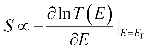 indicates that a large Seebeck coefficient can be obtained if the Fermi energy EF happens to coincide with a steep slope of electron transmission coefficient T(E), which describes the passage of electrons of energy E from the source to the drain of a device. This is a good approximation provided T(E) remains linear in the scale of kBT around Fermi energy where kB is Boltzmann's constant.8
In the past couple of decades, although the thermoelectric performance of the bulk, thin films, and superlattices of Bi, Te, or Sb alloys materials have improved,9 they are not yet sufficiently efficient for future energy demands and furthermore, some of them are toxic with limited global supply.10 Recently the potential of the nanoscale devices composed of organic molecules or 2D materials sandwiched between metallic electrodes was recognized. Molecular-scale devices are particularly interesting, because their transport properties may be tailored by chemical modification of the active part of the device,11–14 varying the contacting configuration,15–17 device architecture18–20 and the Fermi level alignment by gating or doping.21–26 Despite the fact that the nanoelectronic systems are of great interest, it remains a challenge to identify suitable molecules and contacting strategies27,28 which overcome inhomogeneous broadening and junction variability.
Two dimensional materials provide an alternative approach to thermoelectricity in low-dimensional systems. Graphene is the most widely explored 2D material, but is not suitable since the pristine graphene does not have a bandgap and the material has a high in-plane thermal conductance. As an alternative to graphene, transition metal chalcogenides such as monolayer molybdenum disulfide (MoS2) may be attractive alternatives,29,30 since their band gaps could be used to optimise thermoelectricity. Here we show that this is indeed the case for monolayer MoS2, which has a direct bandgap of around 1.6 eV (see Fig. 1 in the ESI†).
Although some contacting strategies have been reported to characterize the electronic and thermoelectric properties of MoS2,20,31 the contacting to metallic electrodes remains a challenge. Recently, it was shown that using a focused electron beam, structures consisting of MoS2 connected directly to Mo6S6 could be formed.32 Mo6S6 nanowires (see Fig. S2 in ESI†) can be used as electrodes, because they possesses metallic properties and a robust structural conformation.33,34 Large scale production of MoS2 nano flakes with self-adaptive Mo6S6 contacts is possible, since their electronic structures are insensitive to the shape of MoS2 monolayers.32 Furthermore, it has been reported that parallel-wire bundles of Mo6S6 nanowires are metallic and mechanically stable.35 Mo6S6 nanowires might therefore be used as a flexible nano wires in electronic devices, because bending does not significantly change their electronic properties.36
Although these junctions have been realized, their potential as thermoelectric devices is unexplored. These devices are advantageous, because they provide new direct and covalent contacting possibilities to MoS2 edges. Furthermore, MoS2 has shown high thermopower and thermoelectric properties using other contacting strategies.20,31 In what follows, we show that flexible routes to tailoring their thermoelectric properties such as doping or gating of both MoS2 and Mo6S6 make such devices very attractive for future thermoelectricity.
Results and discussion
In this letter, we calculate electronic and vibrational properties of MoS2 monolayers connected to Mo6S6 nanowire electrodes (Fig. 1) and show that high Seebeck coefficients and low phononic thermal conductances lead to thermoelectric figures of merit as high as ZT ∼ 2.8. We then demonstrate that thermoelectric properties of these junctions could be tuned by introducing Nb dopants into either MoS2 nano flakes or Mo6S6 electrodes. | ||
| Fig. 1 (a) Schematic of Mo6S6 nanowire–Mo2S–Mo6S6 nanowire junction. (b) The Mo6S6–Mo2S–Mo6S6 junction used in the simulation: yellow atoms represent sulphur and green represents molybdenum. | ||
Fig. 1 shows a thermoelectric device consisting of a central MoS2 monolayer connected to Mo6S6 nanowires as current-carrying leads. The device geometry is similar to that obtained experimentally32 by steering a focused electron beam onto a single MoS2 monolayer. After making holes in the monolayer, the remaining slab reconstructs to form self-adaptive Mo6S6 leads contacted to MoS2 nano flakes.32
Fig. 2 shows the electron transmission coefficient obtained from the density-functional-theory (DFT) mean field Hamiltonian of the converged ground state geometry of the device (see methods for more details) shown in the Fig. 1b. There exists a transmission gap of approximate 1.65 eV for electron energies E between −0.55 eV and 1.1 eV (relative to the DFT-predicted Fermi energy EDFTF). This is due to the gap of the pristine two-dimensional Mo2S (see Fig. S1 in the ESI†) and is in good in agreement with previous studies.30,37 It is known that a step-like transmission coefficient can lead to a high Seebeck coefficient, provided the Fermi energy EF lies close to such steps.8,38 In our case, the step like transmission functions around EF − EDFTF = −0.55 eV and 1.1 eV are due to the valance and conduction bands of MoS2.
 | ||
| Fig. 2 Electron transmission of the junction in Fig. 1. | ||
From the transmission function in Fig. 2, the conductance, the Seebeck coefficient, the thermal conductance due to the electrons and electronic thermoelectric figure of merit  can be obtained (see methods). Fig. 3a shows the electrical conductance for different Fermi energies at room temperature. Due to the thermal averaging of T(E) around −0.55 eV and 1.1 eV, two peaks are obtained around these energies. They also have high slope and therefore, a high Seebeck coefficient is also obtained around these energies (Fig. 3b). Fig. 3c and d show the electronic thermal conductance and the electronic contribution to the figure of merit ZTe. Fig. 3d depicts the variation of ZTe with the Fermi energy. There appear three large resonances up to 50, 100 and 80 around −0.5, 0.5 and 1 eV. In Fig. 3, the red solid curves are exact values obtained using eqn (2)–(5). The blue dashed curves show the prediction of the Wiedemann-Franz law, which is valid provided T(E) varies approximately linearly with E near E = EF on the scale of kBT. Although the two are in close agreement, the Wiedemann-Franz law tends to overestimate the thermal conductance due to electrons and therefore underestimate ZTe. However, ZTe neglects the contribution from phonons in the denominator and therefore to obtain the full ZT, we now compute the thermal conductance due to phonons.
 | ||
| Fig. 3 Electronic contribution to thermoelectric properties as a function of the pristine DFT-predicted Fermi energy at 300 K. (a) Electrical conductance G, (b) Seebeck coefficient S, (c) electronic contribution to thermal conductance κe and (d) electronic thermoelectric figure of merit ZTe. | ||
The results of our phonon transport calculation are shown in Fig. 4, where Fig. 4a shows the phonon transmission spectrum and Fig. 4b shows the corresponding phonon thermal conductance. Compared to the electronic thermal conductance within the gap, the phonon (0.044 nW K−1) contribution to thermal conductance is much higher. Consequently, the total ZT is lower than ZTe. As shown in Fig. 5, a value as high as ZT ∼ 2.8 at 300 K is obtained around EF = −0.5 eV, which is higher than unity and higher than currently-reported values for other materials at room temperature.39–41 Two peaks in the thermoelectric figure of merit curve at −0.5 eV and 1 eV are due to two step-like transmission features at −0.5 eV and 1 eV.
 | ||
| Fig. 4 Phonon transmission spectra (a) and the corresponding thermal conductance (b). | ||
 | ||
| Fig. 5 (a) The thermoelectric figure of merit at 300 K for the structure shown in Fig. 1(b). (b)–(d) The thermoelectric figure of merit as a function of temperature for three particular Fermi energies (EF − EDFTF = −0.2 eV, EF − EDFTF = 0 eV, EF − EDFTF = 0.2 eV) for the structure shown in Fig. 1(b). These calculations are valid provided the forces entering the phonon dynamical matrix are harmonic. Anharmonic effects are negligible, provided the temperature does not approach the melting point of the material. The melting point of MoS2 is greater than 1400 K and therefore we have restricted our analysis to approximately half that value. | ||
To demonstrate that the high ZT at EF − EDFTF = −0.5 eV and 1 eV is due to the valence and conduction bands of MoS2 and not an edge effect, we consider other junctions shown in Fig. S3 and S5 in the ESI,† obtained by increasing the size of the sample, changing the edge shape and applying periodic boundary conductions in transverse direction. Fig. S3–S5† show that their corresponding transmission coefficients possess two main features: step-like transmission features associated with the valence and conduction bands of the MoS2 monolayer around E = −0.5 eV and 1 eV and sharp resonances with small width inside the gap. Local density of states calculations around the DFT Fermi energy (Fig. S4 in the ESI†) reveal that these resonances are due to localized states at the edges of MoS2 and are sensitive to the shape of the edges and size of the flake. However, the features due to the valence and conduction bands of MoS2 are resilient and are less dependent on the details of the junction. Furthermore, the transmission amplitude and slope is higher close to the conduction and valence band edges, which is promising for an efficient thermoelectric device. High ZT is therefore obtained regardless of the shape of the MoS2 flake as shown in Fig. S8 in the ESI† at EF − EDFTF = −0.5 eV and 1 eV. These results indicate that the higher ZT peak is mainly due to the valence band edge of the MoS2 monolayer and the edge states do not play a significant role.
In reality, the Fermi energy may be determined by extrinsic factors such as doping. Indeed Nb atoms were used in the past to tune the Fermi energy of MoS2 to form a p-type semiconductor.21,23 To demonstrate that in the presence of dopants, a high ZT is accessible in these devices, we now show that in the both Mo6S6 electrodes and MoS2 flakes, Nb doping can be used to shift the position of the valence band edge towards the Fermi energy. Fig. S9 of the ESI† shows results for six different dopant configurations. By replacing Mo atoms by Nb substituents in the monolayer MoS2 flake, the Fermi level shifts towards the valence band and simultaneously new transmission peaks due to defect states near the valence band are formed. The precise value of ZT is sensitive to the positions and concentration of the dopants, because multiple scattering of electrons between dopants placed in the different locations, causes the transmission coefficient to change (Fig. S9 in the ESI†). In a real device consisting of many structures such Fig. 1b and Fig S9,† placed in parallel, the ensemble average of transport coefficients are relevant, as defined by the equations in section 10 of the ESI.†Fig. 6a shows the resulting ensemble averaged figure of merit ZTavversus Fermi energy at one particular temperature and Fig. 6(b–d) show ZTav as a function of temperature for three different Fermi energies. Fig. 6b shows that even after allowing for inhomogeneous broadening due to random locations of dopants, room temperature values of ZTav = 0.6 are possible, increasing to 0.8 at 500 K.
 | ||
| Fig. 6 (a) The ensemble average of the total thermoelectric figure of merit at 300 K for the configurations with p-type dopants Nb replacing Mo atoms in ESI Fig. S9.† (b)–(d) The ensemble average of the total thermoelectric figure of merit as the function of temperature when EF − EDFTF = −0.2 eV, EF − EDFTF = 0 eV, EF − EDFTF = 0.2 eV for the configurations with p-type dopants Nb replacing Mo atoms in ESI Fig. S9.† | ||
Conclusion
In summary, we have studied electron and phonon transport through MoS2 nano flakes with self-adaptive Mo6S6 contacts and demonstrated that large Seebeck coefficients and electrical conductance, combined with low thermal conductance due to electrons and phonons lead to large room temperature thermoelectric figures of merit up to 2.8. Even after allowing for inhomogeneous broadening due to random locations of dopants, room temperature values of ZTav = 0.6 are possible, increasing to 0.8 at 500 K. This demonstrates that MoS2 nano flakes are an attractive material for the design of high efficiency, nanoscale, thermoelectric energy harvesters and conversely for nanoscale Peltier cooling.Computational methods
The structures of Mo2S–Mo6S6 junction obtained in the experiments32 were optimized using the first-principles DFT code SIESTA42 with a double-ζ (DZ) basis set. Subsequently, the nanoscale Mo6S6–Mo2S–Mo6S6 sandwich device was constructed. From the relaxed xyz coordinates of the system, sets of xyz coordinates were generated by displacing each atom in positive and negative x, y, and z directions by δq′ = 0.01 Å. The forces in three directions qi = (xi, yi, zi) on each atom were then calculated by DFT without geometry relaxation. These values of forces were combined with the method described in ref. 7 to calculate the dynamical matrix and thermal conductance due to phonons. Furthermore, the mean-field Hamiltonian and overlap matrices were extracted from the first-principles calculation and used to obtain the thermoelectric properties of the devices using Gollum.43 The electron transmission coefficient T(E) as a function of energy is calculated through the formula:| T(E) = Tr[ΓR(E)GR(E)ΓL(E)GR†(E)] | (1) |
| G = G0L0 | (2) |
 | (3) |
 | (4) |
 | (5) |
 | (6) |
 | (7) |
The electrical conductance G, Seebeck coefficient S and thermal conductance due to electrons κe can be combined to obtain electronic thermoelectric figure of merit ZTe. By including the thermal conductance due to phonons κp, the total thermoelectric figure of merit ZT is calculated. T is the mean temperature (T1 + T2)/2, G0 = 2e2/h is the conductance quantum; h is the Planck's constant; e is the charge of electron; f(E) = (1 + exp(E − EF/kBT))−1 is the Fermi–Dirac probability distribution function and EF is the Fermi energy. The relationship between ZT and the power efficiency is discussed in section 11 of the ESI.†
Author information
HS and CJL conceived and conducted the project. Q. W. and H. S. carried out the calculations. All authors took part in the discussions and writing the manuscript.Conflicts of interest
There are no conflicts to declare.Acknowledgements
H. S. acknowledges the Leverhulme Trust for Leverhulme Early Career Fellowship no. ECF-2017-186. Further support from the UK EPSRC is acknowledged, through grant no. EP/M014452/1, EP/P027156/1, EP/N017188/1 and EP/N03337X/1. Support from the European Commission is provided by the FET Open project 767187 – QuIET.Notes and references
- A. L. Moore and L. Shi, Emerging challenges and materials for thermal management of electronics, Mater. Today, 2014, 17, 163–174 CrossRef CAS.
- Y. Kim, W. Jeong, K. Kim, W. Lee and P. Reddy, Electrostatic control of thermoelectricity in molecular junctions, Nat. Nanotechnol., 2014, 9, 881–885 CrossRef CAS PubMed.
- J. R. Widawsky, P. Darancet, J. B. Neaton and L. Venkataraman, Simultaneous determination of conductance and thermopower of single molecule junctions, Nano Lett., 2012, 12, 354–358 CrossRef CAS PubMed.
- H. Sadeghi, S. Sangtarash and C. J. Lambert, Electron and heat transport in porphyrin-based single molecule transistors with electro-burnt graphene electrodes, Beilstein J. Nanotechnol., 2015, 6, 1413–1420 CrossRef CAS PubMed.
- P. Reddy, S. Jang, R. A. Segalman and A. Majumdar, Thermoelectricity in molecular junctions, Science, 2007, 315, 1568–1571 CrossRef CAS PubMed.
- C. A. Perroni, D. Ninno and V. Cataudella, Electron-vibration effects on the thermoelectric efficiency of molecular junctions, Phys. Rev. B: Condens. Matter Mater. Phys., 2014, 90, 275303 CrossRef.
- H. Sadeghi, S. Sangtarash and C. J. Lambert, Oligoyne Molecular Junctions for Efficient Room Temperature Thermoelectric Power Generation, Nano Lett., 2015, 15, 7467–7472 CrossRef CAS PubMed.
- C. J. Lambert, H. Sadeghi and Q. H. Al-galiby, Quantum-interference-enhanced thermoelectricity in single molecules and molecular films, C. R. Phys., 2016, 17, 1084–1095 CrossRef CAS.
- X. Zhang and L. Zhao, Thermoelectric materials: Energy conversion between heat and electricity, J. Mater., 2015, 1, 92–105 Search PubMed.
- L. E. Bell, Cooling, heating, generating power, and recovering waste heat with thermoelectric systems, Science, 2008, 321, 1457–1461 CrossRef CAS PubMed.
- Q. H. Al-Galiby, H. Sadeghi, L. A. Algharagholy, I. Grace and C. Lambert, Tuning the thermoelectric properties of metallo-porphyrins, Nanoscale, 2016, 8, 2428–2433 RSC.
- M. Noori, H. Sadeghi and C. J. Lambert, High-performance thermoelectricity in edge-over-edge zinc-porphyrin molecular wires †, Nanoscale, 2017, 9, 5299–5304 RSC.
- S. V. Aradhya and L. Venkataraman, Single-molecule junctions beyond electronic transport, Nat. Nanotechnol., 2013, 8, 399 CrossRef CAS PubMed.
- M. L. Perrin, R. Frisenda, M. Koole, J. S. Seldenthuis, J. A. C. Gil, H. Valkenier, J. C. Hummelen, N. Renaud, F. C. Grozema, J. M. Thijssen, D. Dulić and S. J. H. van der Zant, Large negative differential conductance in single-molecule break junctions, Nat. Nanotechnol., 2014, 9, 830–834 CrossRef CAS PubMed.
- F. Schwarz and E. Lörtscher, Break-junctions for investigating transport at the molecular scale, J. Phys.: Condens. Matter, 2014, 26, 474201 CrossRef PubMed.
- P. Moreno-García, M. Gulcur, D. Z. Manrique, T. Pope, W. Hong, V. Kaliginedi, C. Huang, A. S. Batsanov, M. R. Bryce, C. Lambert and T. Wandlowski, Single-molecule conductance of functionalized oligoynes: Length dependence and junction evolution, J. Am. Chem. Soc., 2013, 135, 12228–12240 CrossRef PubMed.
- H. Sadeghi, S. Sangtarash and C. J. Lambert, Robust molecular anchoring to graphene electrodes, Nano Lett., 2017, 17, 4611–4618 CrossRef CAS PubMed.
- M. Noori, H. Sadeghi, Q. Al-Galiby, S. W. D. Bailey and C. J. Lambert, High cross-plane thermoelectric performance of metallo-porphyrin molecular junctions, Phys. Chem. Chem. Phys., 2017, 19, 17356–17359 RSC.
- Q. Wu, H. Sadeghi, V. M. García-Suárez, J. Ferrer and C. J. Lambert, Thermoelectricity in vertical graphene-C60-graphene architectures, Sci. Rep., 2017, 7, 11680 CrossRef PubMed.
- H. Sadeghi, S. Sangtarash and C. J. Lambert, Cross-plane enhanced thermoelectricity and phonon suppression in graphene/MoS 2 van der Waals heterostructures, 2D Mater., 2017, 4, 15012 CrossRef.
- K. Dolui, I. Rungger, C. Das Pemmaraju and S. Sanvito, Possible doping strategies for MoS2 monolayers: An ab initio study, Phys. Rev. B: Condens. Matter Mater. Phys., 2013, 88, 075420 CrossRef.
- Q. H. Al-Galiby, H. Sadeghi, D. Z. Manrique and C. J. Lambert, Tuning the Seebeck coefficient of naphthalenediimide by electrochemical gating and doping, Nanoscale, 2017, 9, 4819–4825 RSC.
- S. Gemming, G. Seifert and I. Vilfan, Li doped Mo6S6 nanowires: Elastic and electronic properties, Phys. Status Solidi B, 2006, 243, 3320–3324 CrossRef CAS.
- M. Ghorbani-Asl, A. N. Enyashin, A. Kuc, G. Seifert and T. Heine, Defect-induced conductivity anisotropy in MoS 2 monolayers, Phys. Rev. B: Condens. Matter Mater. Phys., 2013, 88, 245440 CrossRef.
- H. Sadeghi, S. Sangtarash and C. J. Lambert, Enhanced thermoelectric efficiency of porous silicene nanoribbons, Sci. Rep., 2015, 5, 9514 CrossRef CAS PubMed.
- R. Gillen, J. Robertson and J. Maultzsch, Indirect doping effects from impurities in MoS2/h-BN heterostructures, Phys. Rev. B: Condens. Matter Mater. Phys., 2014, 90, 75437 CrossRef.
- W. Hong, D. Z. Manrique, P. Moreno-García, M. Gulcur, A. Mishchenko, C. J. Lambert, M. R. Bryce and T. Wandlowski, Single molecular conductance of tolanes: Experimental and theoretical study on the junction evolution dependent on the anchoring group, J. Am. Chem. Soc., 2012, 134, 2292–2304 CrossRef CAS PubMed.
- Q. Wu, X. Zheng, X. Shi, J. Lan, H. Hao and Z. Zeng, Electron transport enhanced by electrode surface reconstruction: a case study of C 60 -based molecular junctions, RSC Adv., 2014, 4, 44718–44725 RSC.
- C. K. Gan, Theoretical study of thermoelectric properties of few-layer MoS2 and WSe2. Phys, Chem. Chem. Phys., 2014, 16, 10866–10874 RSC.
- E. S. Kadantsev and P. Hawrylak, Electronic structure of a single MoS 2 monolayer, Solid State Commun., 2012, 152, 909–913 CrossRef CAS.
- J. Wu, H. Schmidt, K. K. Amara, X. Xu, G. Eda and B. Özyilmaz, Large thermoelectricity via variable range hopping in chemical vapor deposition grown single-layer MoS2, Nano Lett., 2014, 14, 2730–2734 CrossRef CAS PubMed.
- J. Lin, O. Cretu, W. Zhou, K. Suenaga, D. Prasai, K. I. Bolotin, N. T. Cuong, M. Otani, S. Okada, A. R. Lupini, J.-C. Idrobo, D. Caudel, A. Burger, N. J. Ghimire, J. Yan, D. G. Mandrus, S. J. Pennycook and S. T. Pantelides, Flexible metallic nanowires with self-adaptive contacts to semiconducting transition-metal dichalcogenide monolayers, Nat. Nanotechnol., 2014, 9, 436–442 CrossRef CAS PubMed.
- A. Leen, S. Nano and S. Facilities, Torsional Deformations in Sub-Nanometer MoS Interconnecting Wires, Nano Lett., 2015, 16, 1210–1217 Search PubMed.
- B. Radisavljevic, A. Radenovic, J. Brivio, V. Giacometti and A. Kis, Single-layer MoS2 transistors, Nat. Nanotechnol., 2011, 6, 147–150 CrossRef CAS PubMed.
- J. Kibsgaard, A. Tuxen, M. Levisen, E. Levisen, S. Gemming, G. Seifert, J. V. Lauritsen and F. Besenbacher, Atomic-scale structure of Mo6S6 nanowires, Nano Lett., 2008, 8, 3928–3931 CrossRef CAS PubMed.
- I. Popov, S. Gemming, S. Okano, N. Ranjan and G. Seifert, Etectromechanical switch based on Mo6S6 nanowires, Nano Lett., 2008, 8, 4093–4097 CrossRef CAS PubMed.
- D. Costanzo, S. Jo, H. Berger and A. F. Morpurgo, Gate-induced superconductivity in atomically thin MoS2 crystals, Nat. Nanotechnol., 2016, 11, 339–344 CrossRef CAS PubMed.
- H. Sadeghi, S. Sangtarash and C. J. Lambert, Enhancing the thermoelectric figure of merit in engineered graphene nanoribbons, Beilstein J. Nanotechnol., 2015, 6, 1176–1182 CrossRef CAS PubMed.
- H. Liu, X. Shi, F. Xu, L. Zhang, W. Zhang, L. Chen, Q. Li, C. Uher, T. Day and G. J. Snyder, Copper ion liquid-like thermoelectrics, Nat. Mater., 2012, 11, 422–425 CrossRef CAS PubMed.
- L. Han, D. V. Christensen, A. Bhowmik, S. B. Simonsen, L. T. Hung, E. Abdellahi, Y. Z. Chen, N. V. Nong, S. Linderoth and N. Pryds, Scandium-doped zinc cadmium oxide as a new stable n-type oxide thermoelectric material, J. Mater. Chem. A, 2016, 4, 12221–12231 CAS.
- R. Chetty, A. Bali and R. C. Mallik, Tetrahedrites as thermoelectric materials: an overview, J. Mater. Chem. C, 2015, 3, 12364–12378 RSC.
- J. M. Soler, E. Artacho, J. D. Gale, A. Garcìa, J. Junquera, P. Ordejòn and D. Sànchez-Portal, SIESTA Method For Ab Initio Order-N Materials Simulation, J. Phys.: Condens. Matter, 2002, 14, 2745–2779 CrossRef CAS.
- J. Ferrer, C. J. Lambert, V. M. García-Suárez, D. Z. Manrique, D. Visontai, L. Oroszlany, R. Rodríguez-Ferradás, I. Grace, S. D. Bailey, K. Gillemot, H. Sadeghi and L. A. Algharagholy, GOLLUM: A next-generation simulation tool for electron, thermal and spin transport, New J. Phys., 2014, 16, 093029 CrossRef.
Footnote |
| † Electronic supplementary information (ESI) available. See DOI: 10.1039/c8nr01635f |
| This journal is © The Royal Society of Chemistry 2018 |