DOI:
10.1039/C8NR01527A
(Paper)
Nanoscale, 2018,
10, 13607-13616
Understanding quantum emitters in plasmonic nanocavities with conformal transformation: Purcell enhancement and forces
Received
22nd February 2018
, Accepted 19th June 2018
First published on 25th June 2018
Abstract
Nanogaps supporting cavity plasmonic modes with unprecedented small mode volume are attractive platforms for tailoring the properties of light–matter interactions at the nanoscale and revealing new physics. Hitherto, there is a concerning lack of analytical solutions to divide the complex interactions into their different underlying mechanisms to gain a better understanding that can foster enhanced designs. Bowtie apertures are viewed as an effective and appealing nanocavity and are studied here within the analytical frame of conformal transformation. We show how the non-radiative Purcell enhancement of a quantum emitter within the bowtie nanocavity depends strongly not only on the geometry of the nanocavity, but also on the position and orientation of the emitter. For a 20 nm diameter (∅ 20 nm) bowtie nanocavity, we report a change of up to two orders of magnitude in the maximum non-radiative Purcell enhancement and a shift in its peak wavelength from green to infra-red. The changes are tracked down to the overlap between the emitter field and the gap plasmon mode field distribution. This analysis also enables us to understand the self-induced trapping potential of a colloidal quantum dot inside the nanocavity. Since transformations can be cascaded, the technique introduced in this work can also be applied to a wide range of nanocavities found in the literature.
Introduction
Plasmonics is a thriving research field that has created transformative opportunities for a wide range of applications, spanning from spectroscopy to photothermal therapy.1 The intrinsic nanoscopic volume and high sensitivity to the local environment of surface plasmon modes enable label-free molecular detection.2–5 The large near-field intensity gradients in plasmonic structures yield amplified optical forces that can be used for nanoparticle manipulation (i.e., nanotweezers).6–10 These strong electromagnetic fields also allow weak nonlinear processes, which are governed by the local field, to be notably enhanced.11–14 The ability of plasmons to surpass the diffraction limit is used to produce super-resolution images and to push the resolution of nanolithography.15–19 By the proper engineering of plasmonic structures, light can be trapped and absorbed efficiently in thin-film solar cells.20,21 Gold nanoparticles convert efficiently photon energy into local heat that is used for selective tumour apoptosis.22
Benefitting from the advancements in nanofabrication and the possibility of creating metal–insulator–metal configurations supporting gap plasmon modes, plasmonics is also becoming a fascinating platform to study the nanoscale world.23–26 In this quest, the preferred cavity is the so-called particle(s)-on-a-mirror,5,27–31 but apertures in metals have also their own merits. As far as spectroscopy and trapping are concerned, apertures can remove large background signals and are a natural trapping environment.2,6,9,10,32–34
Nowadays, to design plasmonic nanostructures for specific applications and to build knowledge from experimental observations, scientists rely strongly on a heavy computational burden35 since analytical solutions are limited to simple geometries like spheres.36 The challenge lies then in mapping the plasmon resonances and the corresponding field distributions analytically for the more complex nanostructures and assemblies whereby physical understanding can be gained and a blueprint for the design of new plasmonic nanostructures is provided. An analytical tool that holds promise in this regard is transformation optics.37,38 It has been championed for open-crescent-shaped39–41 and several dimer nanoantennas (e.g., spheres,42 cylinders,43 cylindrical sectors,44 bowties45 and tripods46), but its application in nanocavities is limited to canonical ring-disk and crescent-shaped nanocavities.37,47,48
Motivated by the lack of analytical solutions in plasmonic nanocavities and the increasing use of bowtie nanocavities for trapping and molecular fluorescence,2,9,10,33 we report here an analytical solution for the Purcell enhancement and forces experienced by an emitter (e.g., colloidal quantum dot, QD) inside a two-dimensional (2D) bowtie nanocavity (i.e., a 3D bowtie nanocavity with z-invariance). The study of bowtie nanocavities is timely given their popularity in the community arisen from their stronger field concentration and hence field enhancement at their centre as well as their strong coupling to light compared to other nanocavities.2,9
Analytical framework
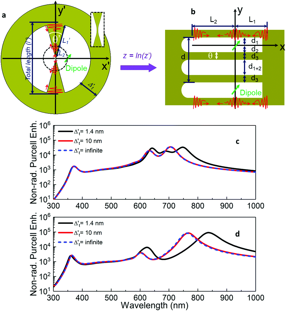
A schematic of the bowtie nanocavity to be investigated in this manuscript can be found in Fig. 1a. Note that it can be understood as a ring-bowtie nanoantenna or as a mirror-image nanoepsilon.49 Without loss of generality, gold is considered for the metal parts of the nanocavity. L′1 and L′2 correspond to the distances from the bowtie nanocavity inner arms (radius of 10 nm) and the 0.5 mm long connecting taper to a circumference of radius 1 nm, as shown in Fig. 1a. The ring width is chosen to be Δ′t = 10 nm to avoid plasmon hybridization50 in the ring, as is demonstrated in Fig. 1c and d. Effectively, this is equivalent to having a single nanocavity embedded in gold; hence, Δ′t = 10 nm and Δ′t = infinite match in Fig. 1c and d. The flare angle θ′ will be varied throughout the manuscript. The gradual connection between the metal inner parts (i.e., the taper) follows a Bézier polygon starting at 0.5 nm from the centre of the nanocavity. The position and orientation of the point (e.g., dimensionless) dipole source (translationally invariant along the out-of-plane direction) mimicking a nanoemitter inside the bowtie nanocavity will be also varied.
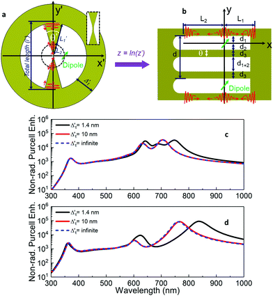 |
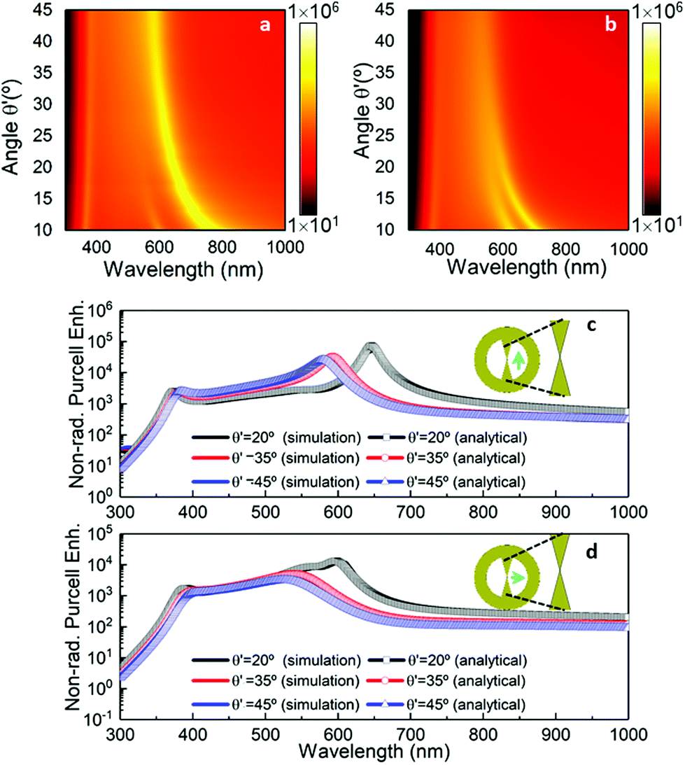
| | Fig. 1 (a) A nanoemitter inside a mirror-image gold nanoepsilon (i.e., bowtie nanocavity). (b) The corresponding transformed space obtained after applying the conformal mapping indicated in the figure. (c, d) Numerical results of the non-radiative Purcell enhancement for different values of Δ′t when the dipole is oriented horizontally (c) and vertically (d). | |
Since the diameter of the nanocavity is l′ = 20 nm ≪ λ0, the problem can be treated quasi-statically. In this scenario, the electric and magnetic fields are decoupled and the former can be completely described by an electrostatic potential satisfying Laplace's equation ∇2φ′(x′, y′) = 0.
The bowtie nanocavity shown in Fig. 1a can be transformed into the geometry shown in Fig. 1b by applying the conformal transformation z = ln(z′/a).11,45,46 Here z = x + iy and z′ = x′ + iy′ correspond to the spatial coordinates in the transformed and original frames, respectively, and a is the distance between the emitter and the origin of the coordinates. With this conformal mapping, the arbitrary oriented line dipole source and the bowtie nanocavity are transformed into a periodic multislab structure with an array of line dipoles located every two slabs. Hence, the periodic unit cell (with a 2π periodicity along the y axis) consists of an array of line dipoles and two metallic slabs (connected at their ends). The dimensions of the metallic slabs are defined by L1 + L2 and θ (= d3) along the x and y axes, respectively.
An important consequence of the quasi-static treatment of the nanocavity and the applied conformal mapping that preserves the local angles is that the material properties are identical in both transformed and original frames. Additionally, the potential is preserved ϕ(x,y) = ϕ′(x′,y′) in both scenarios, respectively.37 Hence, the underlying physics governing Fig. 1a is identical to that of Fig. 1b. Given its canonical form, the description of the latter is simpler and, thus, is given next. From Fig. 1b one can expect that the array of dipoles will excite surface plasmons (SPs) propagating along the x axis. Since the slabs have finite length (L1 and L2), the SPs will be reflected back and forth, producing standing-wave patterns that one can identify to localized surface plasmon (LSP) modes, i.e., the eigen-modes of the system. Because of the small size of the nanocavity compared to the incident wavelength, radiation losses are negligible and the energy pumped into the system by the emitter is dissipated into the metal due to absorption. The quantitative results will be shown and discussed in the following sections and the complete analytical solution in the transformed space can be found in the Methods section.
Results and discussion
The number and spectral position of localized surface plasmon modes
The resonant performance of the bowtie nanocavity can be evaluated analytically by simply solving the problem in the periodic multislab frame.44–46,51 Because of the finite physical size of the nanostructure under study, the LSP modes for the bowtie nanocavity will be distributed in the spectrum at discrete wavelengths satisfying the following resonant condition (see the Methods section for more details):| |  | (1) |
where εAu(ω) is the permittivity of gold, ω = 2πc/λ0 is the angular frequency, c is the velocity of light in vacuum, λ0 is the operational wavelength and k is the angular momentum for each LSP mode defined as k = (nπ – Δφ)(L1 + L2)−1 (with n = 1, 2, 3…). Δφ is the extra phase required to take into account non-perfect reflections of the SP modes at both ends of the metallic slabs along the x axis (see the Methods section).
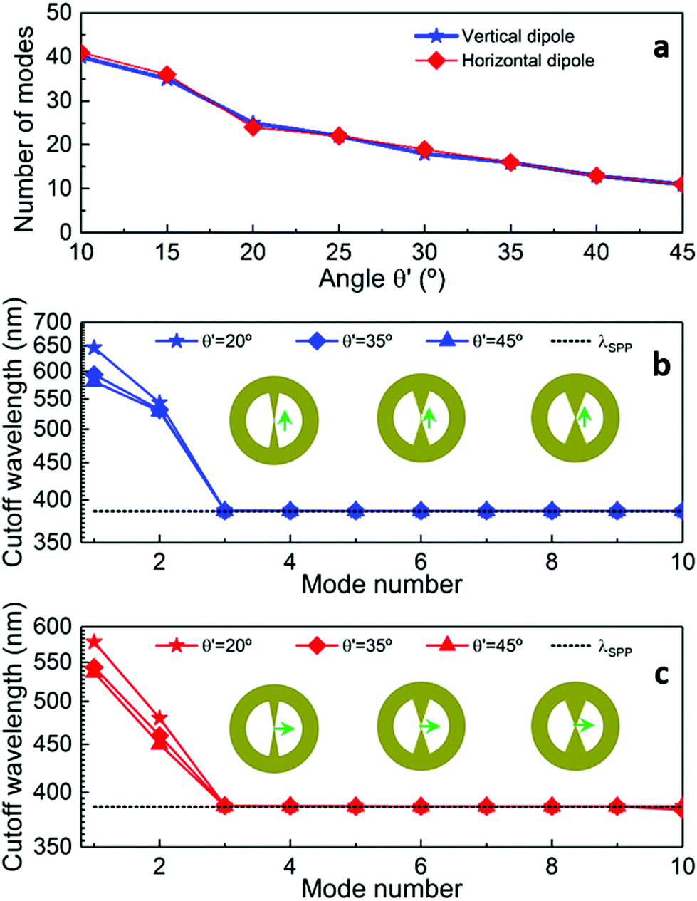
By applying the above resonant condition, the number of LSP modes supported by the bowtie nanocavity as a function of the angular aperture of the arms (θ′ = θ = d3) are shown in Fig. 2a for vertical and horizontal emitter orientations. As observed, the number of modes increases for smaller θ′. This is an expected result since there is a clear dependence on the dimension θ′ (= d3) for fixed L1 and L2, in agreement with our recent findings for bowtie nanoantennas.45,51 To further study the plasmonic resonances of the nanocavity, the spectral distributions of the first 10 LSP modes for nanocavities with θ′ = 20°, 35° and 45° under vertical and horizontal emitter orientations are depicted in Fig. 2b and c, respectively. As is shown, the LSP modes are located within the entire visible spectrum and they are blue shifted when θ′ is increased, similarly to canonical multilayer plasmonic systems. Also, it can be observed that higher-order LSP modes (n > 3) are agglomerated close to the SP wavelength λsp. It is worth underlining that the LSP modes are eigen-modes of the nanocavity and their emergence and strength will depend on their field overlap integral to the emitter. The role of the emitter position and orientation will be discussed in the following sections.
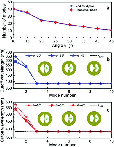 |
| | Fig. 2 (a) The number of LSP modes supported by the nanocavity as a function of θ′ for both vertical and horizontal emitter orientations. (b) Analytical resonant wavelength for the LSP modes supported by bowtie nanocavities with angles θ′ = 20° (stars), 35° (rhombus) and 45° (triangles), excited under vertical (b) and horizontal (c) emitter orientations, as shown in the insets. Note that the discrete points have been connected with solid lines to guide the eye. Horizontal dashed lines mark the λsp. | |
Non-radiative Purcell enhancement and field distribution
Within the conformal transformation and quasi-static formalisms, the power dissipated in the original scenario, P(x′,y′)abs, is identical to that in the transformed space, P(x,y)abs. The latter can be easily calculated by evaluating the electric field at the position of the dipole as 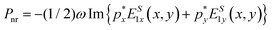 where Pnr is the non-radiative power emission, px and py are x and y components of the dipole moment with magnitude |p|, respectively, and ES1x(x,y) and ES1y(x,y) are the x and y components of the electric field in the region where the dipole is located (see the Methods section for the full analytical expression). Based on this, the non-radiative Purcell enhancement can be calculated as
  where P0(ω) = (1/16)ω3μ0|p|2 is the power radiated by the emitter and μ0 is the permeability of vacuum. It is important to note that, since the nanocavity is evaluated quasi-statically, the extinct power by a point dipole has been used to describe the non-radiative power of the emitter. Moreover, in all the calculations presented here, an intrinsic quantum yield equal to 1 has been used for the emitter in order to be able to relate the non-radiative decay of the emitter with the power absorbed by the nanocavity, Pnr = P(x,yabs) = P(x′,y′)abs.45,46
With this formulation, the analytical results of the non-radiative Purcell enhancement spectra for a bowtie nanocavity with l′ = 20 nm as a function of θ′ (ranging from 10° to 45°) are shown in Fig. 3a and b considering vertical and horizontal emitter orientations, respectively. Here, the emitter is placed at (x′ = 1 nm, y′ = 0) in the original frame [i.e., (x = y = 0) in the multislab geometry]. As observed, the LSP modes are blue shifted when θ′ is increased, in agreement with the results shown in Fig. 2, covering the entire visible spectrum. For instance, the fundamental LSP mode (n = 1) is shifted from (infra-) red ∼770 nm to yellow ∼582 nm when θ′ is modified from 10° to 45°, respectively, under a vertical emitter orientation. Similarly, it is displaced from red ∼707 nm to green ∼527 nm for the same range of θ′ under the horizontal emitter orientation. To better observe this performance, the analytical results of the non-radiative Purcell enhancement spectra for values of θ′ = 20°, 35° and 45° are shown in Fig. 3c and d considering vertical and horizontal emitter orientations, respectively. The analytical results are compared with numerical simulations carried out with the commercial software COMSOL Multiphysics® (see the Methods section) for the original bowtie nanocavity space. The good agreement achieved between analytical and numerical results validates the analytical formulation.
 |
| | Fig. 3 Analytical  for the bowtie nanocavity with varying θ′ under vertical (a) and horizontal (b) emitter orientations. Numerical (solid lines) and analytical (symbols) results comparing the specific bowtie nanocavity with θ′ = 20, 35, and 45° under vertical (c) and horizontal (d) emitter orientations. for the bowtie nanocavity with varying θ′ under vertical (a) and horizontal (b) emitter orientations. Numerical (solid lines) and analytical (symbols) results comparing the specific bowtie nanocavity with θ′ = 20, 35, and 45° under vertical (c) and horizontal (d) emitter orientations. | |
As observed in Fig. 3, the magnitude of the non-radiative Purcell enhancement is different for each emitter orientation and LSP mode. This stems from the different field integral overlap between the emitter and the LSP field mode distribution. The larger the field integral overlap is, the higher the non-radiative Purcell enhancement is. To investigate this in more detail, the results of the field distribution in the bowtie nanocavity for the fundamental (n = 1) and first higher-order (n = 2) LSP modes under vertical and horizontal emitter orientations are shown in Fig. 4 for θ′ = 20°. Note that Ey in the multislab geometry corresponds to the azimuthal component of the electric field (E′φ′) in the original frame, whereas Ex in the multislab geometry relates to the radial component of the electric field (E′ρ′) in the original frame.45,46 Hence, for vertical (Fig. 4a and b) and horizontal emitter orientations (Fig. 4e and f), E′φ′ and E′ρ′ are plotted accordingly. Here, E′φ′ and E′ρ′ are calculated as E′φ′ = −E′x′ sin(φ′) + E′y′ cos(φ′) and E′ρ′ = E′x′![[thin space (1/6-em)]](https://www.rsc.org/images/entities/char_2009.gif) cos(φ′) + E′y′ sin(φ′) with φ′ = tan−1 (y′/x′), respectively.
cos(φ′) + E′y′ sin(φ′) with φ′ = tan−1 (y′/x′), respectively.
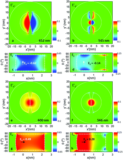 |
| | Fig. 4 Electric field distribution Eϕ′(x′, y′) and Eρ′(x′, y′) of the first two LSP modes for θ′ = 20° under vertical (a, b) and horizontal (e, f) emitter orientations, respectively. Note that the colour scale has been saturated in order to better appreciate the field distribution. The corresponding electric field distributions Ey(x, y) and Ex(x, y) in the transformed space for vertical (c, d) and horizontal (g, h) emitter orientations. | |
Fig. 4 manifests unquestionably the differences between each LSP mode. For either emitter orientation, the first higher-order LSP mode displays an additional antinode in the field distribution compared to the fundamental mode. This is even more evident in the transformed space. For instance, under vertical emitter orientation, Ey at the first peak of  has one antinode in between two nodes at the ends of the nanocavity (Fig. 4c), which corresponds to the first harmonic of the standing-wave pattern, i.e., the field distribution associated with the fundamental n = 1 LSP mode. For the second peak (Fig. 4d) Ey has two antinodes and three nodes, accounting for the second harmonic of the standing-wave pattern, i.e., the n = 2 LSP mode. For the horizontal emitter orientation, two Ex maxima are obtained at both ends with a node in between them at the first peak of
  (Fig. 4g), while the field distribution for the second peak (Fig. 4h) has a node in between a maximum and a minimum at the ends of the nanocavity.
The field representation in the transformed space also assists in the discussion regarding the magnitude of  . For the vertical emitter orientation (Fig. 4a–d), the emitter [at (x′, y′) = (1, 0) in the real space, and (x, y) = (0, 0) in the transformed space] is located at a position where the field strength of the n = 1 LSP mode is larger (Ey = −0.62) than that of the n = 2 LSP mode (Ey = −0.14). The field integral overlap is therefore larger for n = 1, resulting in a higher
  (as shown in Fig. 3c). The same argument applies to the horizontal emitter orientation case (Fig. 4e–h).
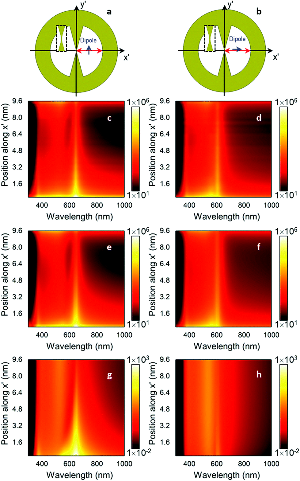
Changing the position of the emitter
To further study the influence of the emitter on  ,
,  is plotted against the emitter position along the x′ axis in Fig. 5c and d under vertical and horizontal emitter orientations, respectively. These analytical results are in agreement with numerical simulations depicted in Fig. 5e and f. The peak of
  related to the fundamental LSP is visible regardless of the emitter orientation and position, but its magnitude is enhanced for positions closer to the centre for vertical emitter orientation, whereas it is more constant for horizontal emitter orientation. Namely, for n = 1 LSP mode,
  is equal to 1.11 × 10⁶, 0.72 × 10³ and 9.5 × 10³ for vertical emitter orientation and 6.45 × 10⁴, 1.3 × 10³ and 1.6 × 10³ for horizontal emitter orientation at x′ = 0.3 nm, x′ = 6.6 nm and x′ = 9.6 nm, respectively. These gradient responses in
  for vertical and horizontal emitter orientations account for the strong and weak asymmetric field distributions of the n = 1 LSP mode in Fig. 4c and g, respectively, and also reflect the significant contribution of higher-order LSP modes for x′ → 0 and 10 nm; emitters placed close to metal boundaries (either by the nanocavity centre or by its outer periphery) couple more efficiently to the higher-order LSP modes that are accumulated at such boundaries (see the wavelength range below 600 nm in Fig. 4c–f).29,42 These additional non-radiative channels contribute to the total
  , yielding an overall increase of the
  baseline.
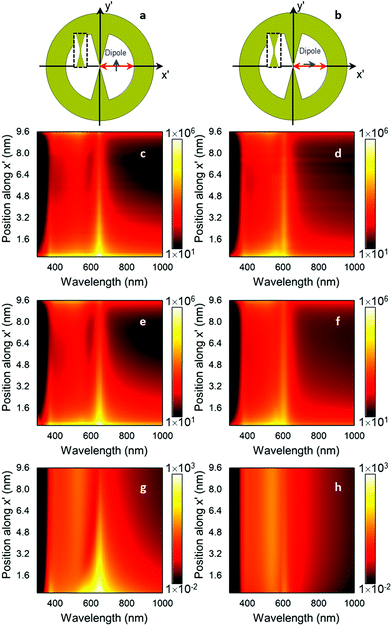 |
| | Fig. 5 Schematic representation of the bowtie nanocavity with a vertical (a) and a horizontal emitter (b). Analytical (c, d) and numerical (e, f)  for the bowtie nanocavity with θ′ = 20° and a vertical (c, e) and a horizontal emitter (d, f) at y′ = 0 and moving along the x′ axis. Numerical for the bowtie nanocavity with θ′ = 20° and a vertical (c, e) and a horizontal emitter (d, f) at y′ = 0 and moving along the x′ axis. Numerical  for vertical (g) and horizontal emitter orientations (h). for vertical (g) and horizontal emitter orientations (h). | |
The impact of the emitter position is more significant for higher-order LSP modes, whose field distributions display nodes across the nanocavity and is enhanced at metal/dielectric interfaces (Fig. 4d and h). These higher-order LSP modes emerge in the spectral range ∼370–570 nm (Fig. 2b and c) and are responsible for the increase in  within such an approximate wavelength range at both ends of the spatial window displayed (Fig. 5c–f).
Additionally, the numerical results of the radiative Purcell spectra  (calculated as the power radiated by the bowtie nanocavity, Pr, normalized to the power radiated by the emitter P0) as a function of the position of the emitter are shown in Fig. 5g and h for vertical and horizontal emitter orientations, respectively. These results show that
  is three orders of magnitude lower than
  , and thus, sustains the initial assumption of the theoretical frame that radiation losses are negligible in the system. From these results, one can also note that higher-order LSP modes have negligible radiative character compared to n = 1 LSP mode, since they are not dipolar in nature unlike the fundamental LSP mode.
For the sake of completeness, the analytical results of the  when the emitter moves along the y′ axis at x′ = 2.6 nm are shown in Fig. 6c and d along with the numerical results (Fig. 6e and f). As observed, the magnitude of the
  for the different LSP modes is enhanced when the emitter is close to the metal (as was shown when the emitter was moved along the x′ axis in Fig. 6c–f). For instance, for the LSP with n = 1, the
  is 8.95 × 10³ and 6.54 × 10⁴ for vertical emitter orientation and 4.22 × 10³ and 2.29 × 10⁴ for horizontal emitter orientation at y′ = 0 nm and y′ = 9.6 nm, respectively. Finally, the results of
  are shown in Fig. 6g and h with, again, values three orders of magnitude lower than
  , as in Fig. 5g and h.
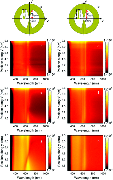 |
| | Fig. 6 Schematic representation of the bowtie nanocavity with a vertical (a) and a horizontal emitter (b). Analytical (c, d) and numerical (e, f)  for the bowtie nanocavity with θ′ = 20° and a vertical (c, e) and a horizontal emitter (d, f) at x′ = 2.6 nm and moving along the y′ axis. Numerical for the bowtie nanocavity with θ′ = 20° and a vertical (c, e) and a horizontal emitter (d, f) at x′ = 2.6 nm and moving along the y′ axis. Numerical  for vertical (g) and horizontal emitter orientations (h). for vertical (g) and horizontal emitter orientations (h). | |
Optical forces
As discussed above, the emitter excites bowtie nanocavity LSP modes. The field distributions induced by such LSP modes inside the nanocavity exert back then an optical force on the emitter. To consider this picture realistically, the emitter is assumed in this section to be a 2 nm diameter (∅ 2 nm) colloidal ZnO QD52,53 and the nanocavity is filled with water (εr = 1.77). Note that the emitter model also takes into account the influence of the emitter on the nanocavity electric field that was neglected previously with the point dipole definition. We calculate the optical force 〈F〉 at the fundamental LSP mode wavelength using the Maxwell stress tensor through the electric field distribution.6 In order to evaluate the stability of the trapping, we compute the potential energy of the colloidal ZnO QD in the field of the nanocavity as  . Given the aqueous environment, Brownian motion should be taken into account. Hence, the potential is normalized to kBT, where kB is the Boltzmann constant and T the temperature, which is taken to be 300 K.
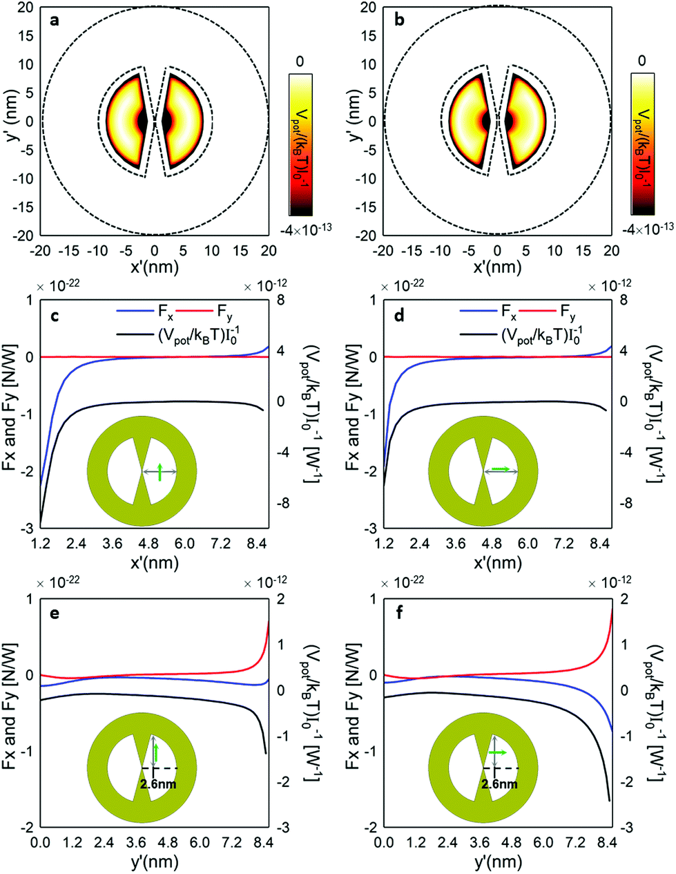
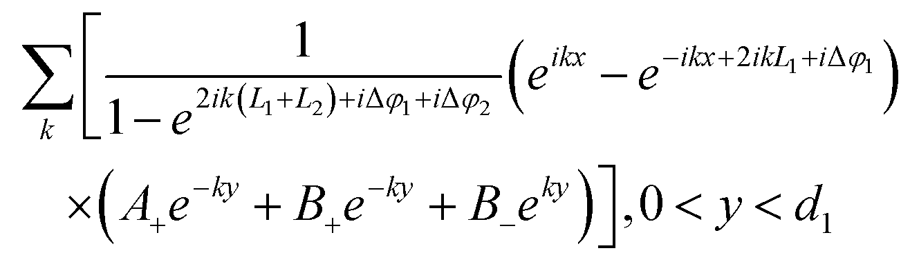
The spatial potential depth for the QD with vertical and horizontally polarized photoluminescence is shown in Fig. 7a and b, respectively. The x′-axis (y′ = 0) and y′-axis (x′ = 2.6 nm) cut is provided in Fig. 7c, d and e, f respectively, along with the optical forces to facilitate the discussion. Stable trapping is expected to occur along the perimeter of the nanocavity, especially close to the centre of the nanocavity where the field gradient is larger. Indeed, since stable trapping often requires a trap depth of ∼10kBT,54 only the centre of the nanocavity and the top and bottom vertexes provide a suitable spot, given the dimensions of the QD. From this, it also follows that an unpolarized QD placed along the x′ = 2.6 nm vertical line will experience a force strong enough to be trapped at y′ = 0 nm (towards the nanoantenna centre). When the QD approaches the nanoantenna vertices, it will also be trapped, but it will lean against the right or left metallic wall depending on the photoluminescence polarization (Fig. 7e and f).
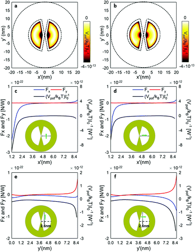 |
| | Fig. 7 (a, b) The normalized self-induced trapping potential distribution of a ∅ 2 nm colloidal ZnO QD inside a θ′ = 20° nanocavity at the LSP resonant wavelength of 779.2 nm – photoluminescence polarized vertically – (a) and 697.7 nm – photoluminescence polarized horizontally – (b). (c, d) Normalized forces along the x (Fx) and y (Fy) axes (blue and red lines, respectively) together with the normalized self-induced trapping potential (black line) calculated at the y′ = 0 horizontal line as shown in the insets for the photoluminescence polarized vertically (c) and photoluminescence polarized horizontally (d). (e, f) Normalized forces along the x (Fx) and y (Fy) axes (blue and red lines, respectively) together with the normalized self-induced trapping potential (black line) calculated at x′ = 2.6 nm vertical line as shown in the insets for the photoluminescence polarized vertically (e) and photoluminescence polarized horizontally (f). | |
Methods
Transformed space
Since the diameter of the Au bowtie nanocavity is significantly smaller than the operational wavelength (l′ ≪ λ0), the quasi-static approximation is applicable. In this scenario, the electric field can be fully described by an electrostatic potential satisfying Laplace's equation. In the geometry shown in Fig. 1b, the emitters are able to excite SP modes in both longitudinal and transversal directions, propagating along the y- and x-axes, respectively. However, since we are interested in calculating the surface plasmon modes for the multislab geometry when L1 + L2 ≪ θ′, the contribution of the longitudinal LSP modes can be neglected and it can be assumed that the excited LSP modes are mainly due to the transversal modes (with a phase variation along the x axis).
With these considerations taken into account, the electrostatic potentials outside and inside the metallic slabs in Fig. 1b can be calculated as the sum of all discrete transverse modes, as follows:
| |  | (2) |
| |  | (3) |
| |  | (4) |
| |  | (5) |
| |  | (6) |
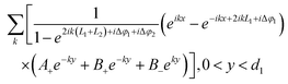
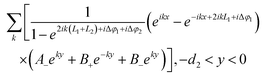
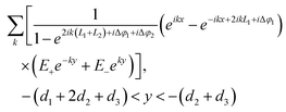
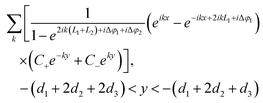
where
A+ and
A− are the expansion coefficients of the incident potential,
B+ and
B− are the coefficients due to the scattering potential in the region where the dipole is present (
d2 <
y <
d1),
E+ and
E− are the coefficients associated with the scattering potential in the region where the dipole is absent (
d2 +
d1) and
C+,
C−,
D+ and
D− are those corresponding to the potential inside the metallic slabs (
d3); Δ
φ1 and Δ
φ2 are the phase corrections accounting for the complex reflection of the SP at the right and left gold walls of the transformed space, respectively;
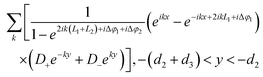
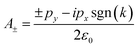
k is the wave number of the transverse LSP modes calculated as:
| |  | (7) |
with
n = 1, 2, 3… representing each discrete LSP mode and Δ
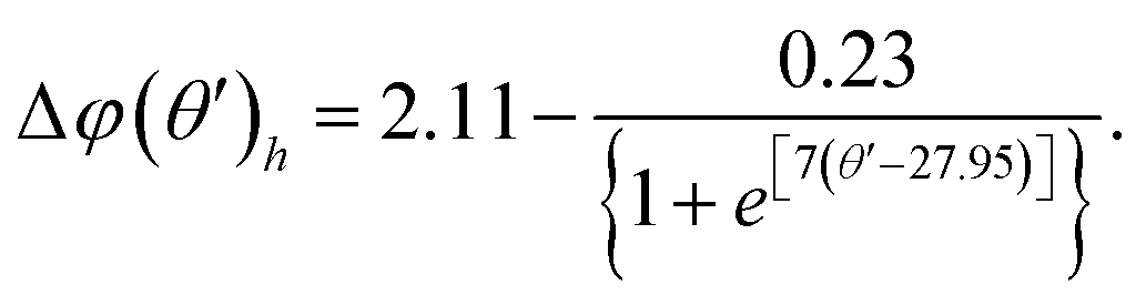
φ as the total phase correction applied to the bowtie nanocavity accounting for the complex reflection of the SP at both ends of the nanostructure as described in the main text. For completeness, the calculated values of Δ
φ for the nanocavities described in
Fig. 3a and b with
θ′ ranging from 10° to 45° under vertical and horizontal emitter orientations are shown in
Fig. 8a and b, respectively. As observed, the higher
θ′ is, the larger the value of Δ
φ is. For each emitter orientation (vertical and horizontal), Δ
φ(
θ′)
v,h can be mathematically described with a sigmoidal function, as follows:
| | 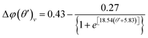 | (8) |
| | 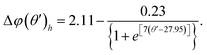 | (9) |
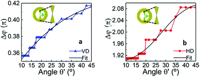 |
| | Fig. 8 Phase correction as a function of θ′ considering a bowtie nanocavity with l′ = 20 nm under vertical (a) and horizontal (b) polarization of the emitter. | |
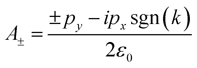
Finally, the coefficients (A+ and A−) related to the incident potential can be calculated by expanding the potential of the dipole emitter along the x direction via a Fourier transform, as follows:
| |  | (10) |
where
px and
py are the two components of the dipole moment along the
x- and
y-axes, respectively, and
ε0 is the permittivity in vacuum.
In order to calculate the coefficients B±, C±, D± and E± in eqn (2)–(6) it is necessary to apply boundary conditions at the metal/dielectric interfaces.
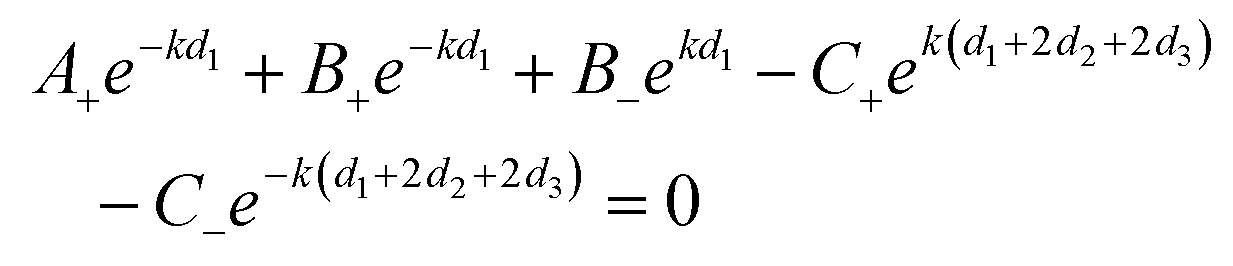
The continuity of the tangential component of the electric field E∥ = Ex at the boundaries d1, d2, d2 + d3 and d1 + 2d2 + 2d3 leads to
| |  | (11) |
| | | A−e−kd2 + B+ekd2 + B−e−kd2 − D+ekd2 − D−e−kd2 = 0 | (12) |
| | 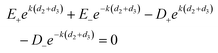 | (13) |
| | 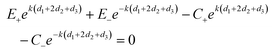 | (14) |
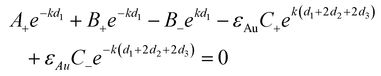
The continuity of the normal component of the displacement current D⊥ = Dy = εAuEy across the same boundaries as the expressions above leads to
| |  | (15) |
| | 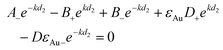 | (16) |
| | 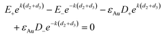 | (17) |
| | 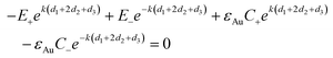 | (18) |
with
εAu being the permittivity of the metal (gold) used in the bowtie nanocavity. For the sake of brevity and due to the complexity of each constant, their solutions are not shown here. However, they can be easily obtained either manually or with the assistance of mathematical software.
The solutions of the potentials in real space for the region where the dipole is present (ϕS1 for d2 < y < d1) and absent (ϕS2 for d2 + d1) can be calculated by applying an inverse Fourier transform to the induced potentials, as follows:
| | 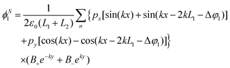 | (19) |
| |  | (20) |
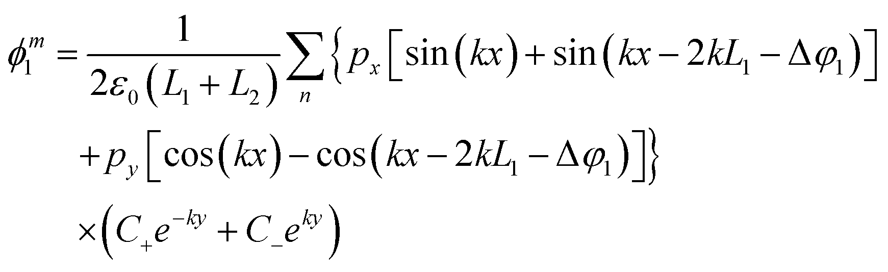
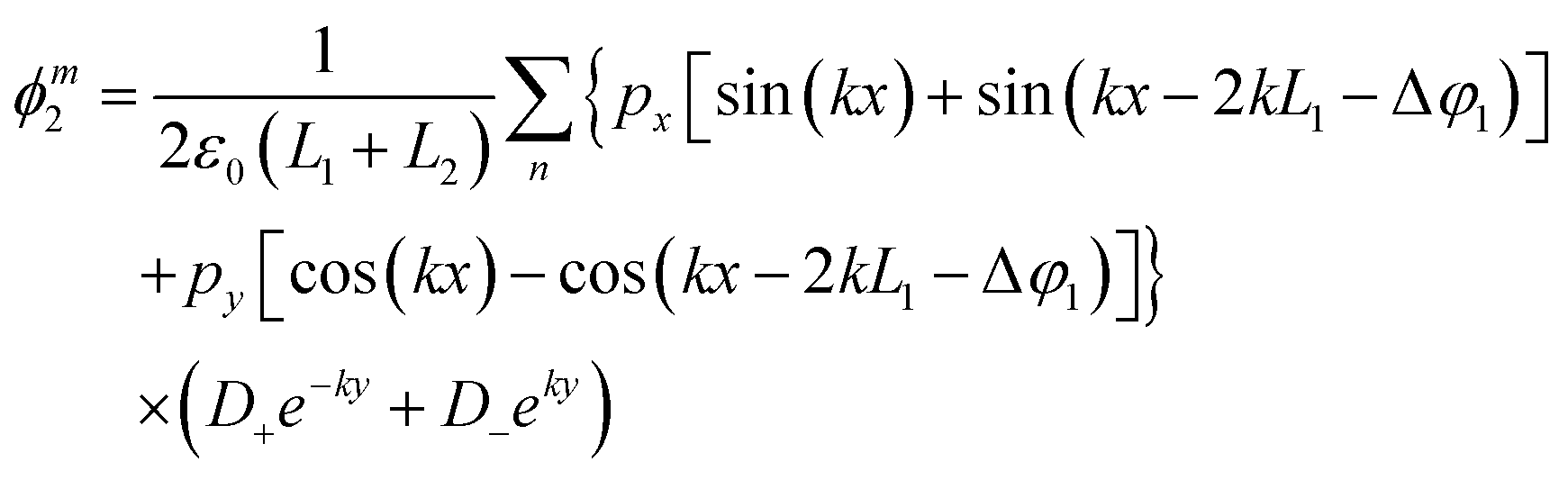
Following the same steps for both metallic slabs, the expressions defining the potentials (ϕm1 and ϕm2, which correspond to the top and bottom arms in the scenario of the bowtie nanocavity) are as follows:
| |  | (21) |
| | 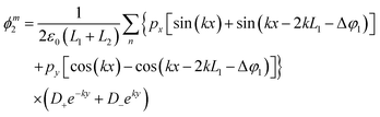 | (22) |
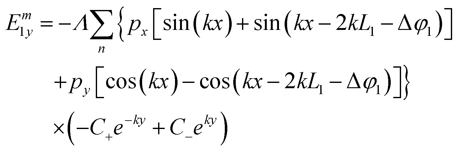
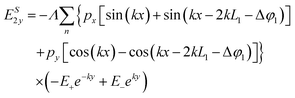
From these results, the x and y components of the electric field outside and inside the metallic slabs can be calculated by simply differentiating the potentials defined in eqn (19)–(22):
| | 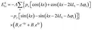 | (23) |
| | 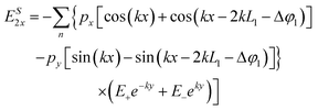 | (24) |
| |  | (25) |
| | 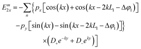 | (26) |
| |  | (27) |
| |  | (28) |
| |  | (29) |
| | 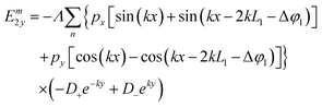 | (30) |
where
Λ =
k/[2
ε0(
L1 +
L2)].
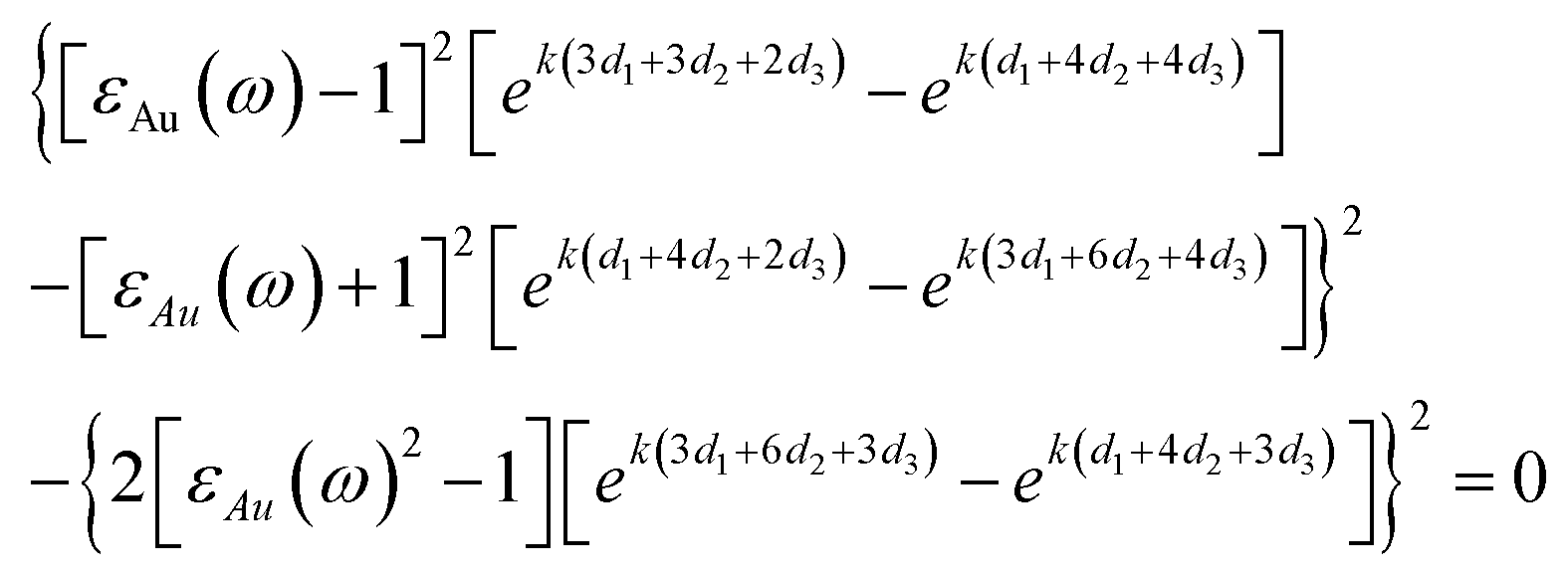
The resonant condition described in eqn (1) is derived taking into account the condition of divergence of the coefficients of the scattered potential (B±) calculated from eqn (11)–(18).
Numerical simulations
The commercial finite element analysis software COMSOL Multiphysics® is used to validate the analytical results. Gold permittivity is modelled using an analytical polynomial equation. This function fits Palik's experimental data.55 The bowtie nanocavities are embedded in vacuum (and gold in one specific case in Fig. 1c and d), modelled as a two-dimensional square 700 nm × 700 nm box enclosed by scattering boundary conditions (i.e., perfectly matched layers). The emitter is modelled using two anti-parallel in-plane magnetic currents with a separation of 5 pm. For the optical forces, the nanocavity is filled with water [εr(600 nm) = 1.77] and the colloidal ZnO QD is modelled as a circle of diameter 2 nm and dielectric function fitting Bodurov's experimental data.56 A fine mesh is used with a maximum and a minimum element size of 2 nm and 3 pm, respectively, within the vacuum region. A refined mesh, twice smaller than in vacuum, is used for gold parts to ensure accurate results.
Conclusions
The conformal transformation technique has been applied to a bowtie nanocavity hosting a nanoemitter in order to describe analytically the non-radiative Purcell enhancement experienced by such local nanoemitters. The non-radiative decay channels in the system are the different LSP modes excited by the emitter. For a ∅ 20 nm gold bowtie nanocavity, multiple LSP modes emerge within the entire visible spectrum whose strength and spectral position depend strongly on the position and orientation of the emitter. The analysis presented here has also enabled us to investigate the self-induced trapping potential of a realistic ∅ 2 nm colloidal ZnO QD inside the ∅ 20 nm gold bowtie nanocavity. The trapping force exceeds the Brownian motion along the perimeter of the bowtie nanocavity regardless of the photoluminescence polarization. The results presented here underline the potential of conformal transformation to unveil the different underlying mechanisms in plasmonic systems and hold promise for outlining design guidelines for plasmonic-based trapping systems. In addition, the methodology can be applied in a straightforward manner to understand the quantum effects in bowtie nanocavities.37 It should be noted that larger bowtie nanocavities have a significant radiative channel and the quasi-static approximation fails. Nevertheless, this study still provides general guidelines to predict qualitatively the forces experienced by a QD inside the nanocavity.
Conflicts of interest
There are no conflicts to declare.
Acknowledgements
V. P.-P. is supported by the Newcastle University [Newcastle University Research Fellow]. M. N.-C. is supported by the University of Birmingham [Birmingham Fellowship].
References
- J. A. Schuller, E. S. Barnard, W. Cai, Y. Chul Jun, J. S. White and M. L. Brongersma, Nat. Mater., 2010, 9, 193 CrossRef PubMed.
- G. Lu, W. Li, T. Zhang, S. Yue, J. Liu, L. Hou, Z. Li and Q. Gong, ACS Nano, 2012, 6, 1438 CrossRef PubMed.
- H. Aouani, H. Šipová, M. Rahmani, M. Navarro-Cía, K. Hegnerová, J. Homola, M. Hong and S. A. Maier, ACS Nano, 2013, 7, 669 CrossRef PubMed.
- H. Aouani, M. Rahmani, H. Šípová, V. Torres, K. Hegnerová, M. Beruete, J. Homola, M. Hong, M. Navarro-Cía and S. A. Maier, J. Phys. Chem. C, 2013, 117, 18620 CrossRef.
- A. R. L. Marshall, J. Stokes, F. N. Viscomi, J. E. Proctor, J. Gierschner, J.-S. G. Bouillard and A. M. Adawi, Nanoscale, 2017, 9, 17415 RSC.
- K. Okamoto and S. Kawata, Phys. Rev. Lett., 1999, 83, 4534 CrossRef.
- M. Righini, P. Ghenuche, S. Cherukulappurath, V. Myroshnychenko, F. J. García de Abajo and R. Quidant, Nano Lett., 2009, 9, 3387 CrossRef PubMed.
- W. Zhang, L. Huang, C. Santschi and O. J. F. Martin, Nano Lett., 2010, 10, 1006 CrossRef PubMed.
- P. Mestres, J. Berthelot, S. S. Aćimović and R. Quidant, Light: Sci. Appl., 2016, 5, e16092 CrossRef.
- M. Shah Alam, F. Karima and C. Zhao, Nanoscale, 2016, 8, 9480 RSC.
- M. Navarro-Cía and S. A. Maier, ACS Nano, 2012, 6, 3537 CrossRef PubMed.
- H. Aouani, M. Navarro-Cía, M. Rahmani, T. P. H. Sidiropoulos, M. Hong, R. F. Oulton and S. A. Maier, Nano Lett., 2012, 12, 4997 CrossRef PubMed.
- M. Kauranen and A. V. Zayats, Nat. Photonics, 2012, 6, 737 CrossRef.
- H. Aouani, M. Rahmani, M. Navarro-Cía and S. A. Maier, Nat. Nanotechnol., 2014, 9, 290 CrossRef PubMed.
- S. Kawata, Y. Inouye and P. Verma, Nat. Photonics, 2009, 3, 388 CrossRef.
- F. Balzarotti and F. D. Stefani, ACS Nano, 2012, 6, 4580 CrossRef PubMed.
- J. L. Ponsetto, F. Wei and Z. Liu, Nanoscale, 2014, 6, 5807 RSC.
- N. Fang, H. Lee, C. Sun and X. Zhang, Science, 2005, 308, 534 CrossRef PubMed.
- W. Srituravanich, L. Pan, Y. Wang, C. Sun, D. B. Bogy and X. Zhang, Nat. Nanotechnol., 2008, 3, 733 CrossRef PubMed.
- H. A. Atwater and A. Polman, Nat. Mater., 2010, 9, 205 CrossRef PubMed.
- S. Mubeen, J. Lee, W.-R. Lee, N. Singh, G. D. Stucky and M. Moskovits, ACS Nano, 2014, 8, 6066 CrossRef PubMed.
- G. Baffou and R. Quidant, Laser Photonics Rev., 2013, 7, 171 CrossRef.
- Z. C. Dong, X. L. Zhang, H. Y. Gao, Y. Luo, C. Zhang, L. G. Chen, R. Zhang, X. Tao, Y. Zhang, J. L. Yang and J. G. Hou, Nat. Photonics, 2010, 4, 50 CrossRef.
- K. J. Savage, M. M. Hawkeye, R. Esteban, A. G. Borisov, J. Aizpurua and J. J. Baumberg, Nature, 2012, 491, 574 CrossRef PubMed.
- K. Santhosh, O. Bitton, L. Chuntonov and G. Haran, Nat. Commun., 2016, 7, 11823 CrossRef PubMed.
- S. Trautmann, J. Aizpurua, I. Götz, A. Undisz, J. Dellith, H. Schneidewind, M. Rettenmayr and V. Deckert, Nanoscale, 2017, 9, 391 RSC.
- G. M. Akselrod, T. Ming, C. Argyropoulos, T. B. Hoang, Y. Lin, X. Ling, D. R. Smith, J. Kong and M. H. Mikkelsen, Nano Lett., 2015, 15, 3578 CrossRef PubMed.
- T. B. Hoang, G. M. Akselrod and M. H. Mikkelsen, Nano Lett., 2016, 16, 270 CrossRef PubMed.
- R. Chikkaraddy, B. de Nijs, F. Benz, S. J. Barrow, O. A. Scherman, E. Rosta, A. Demetriadou, P. Fox, O. Hess and J. J. Baumberg, Nature, 2016, 535, 127 CrossRef PubMed.
- F. Benz, M. K. Schmidt, A. Dreismann, R. Chikkaraddy, Y. Zhang, A. Demetriadou, C. Carnegie, H. Ohadi, B. de Nijs, R. Esteban, J. Aizpurua and J. J. Baumberg, Science, 2016, 354, 726 CrossRef PubMed.
- G.-C. Li, Y.-L. Zhang, J. Jiang, Y. Luo and D. Y. Lei, ACS Nano, 2017, 11, 3067 CrossRef PubMed.
- D. Punj, M. Mivelle, S. B. Moparthi, T. S. van Zanten, H. Rigneault, N. F. van Hulst, M. F. García-Parajo and J. Wenger, Nat. Nanotechnol., 2013, 8, 512 CrossRef PubMed.
- A. A. Al Balushi, A. Zehtabi-Oskuie and R. Gordon, Biomed. Opt. Express, 2013, 4, 1504 CrossRef PubMed.
- Y. Zhao, D. Chen, H. Yue, M. M. Spiering, C. Zhao, S. J. Benkovic and T. J. Huang, Nano Lett., 2014, 14, 1952 CrossRef PubMed.
- B. Gallinet, J. Butet and O. J. F. Martin, Laser Photonics Rev., 2015, 9, 577 CrossRef.
-
C. F. Bohren and D. R. Huffman, Absorption and Scattering of Light by Small Particles, Wiley-VCH Verlag GmbH, Weinheim, Germany, 1998 Search PubMed.
-
A. Aubry and J. B. Pendry, Active Plasmonics and Tunable Plasmonic Metamaterials, John Wiley & Sons, Hoboken, NJ, US, 2013, ch. 4, pp. 105–152 Search PubMed.
- L. Xu and H. Chen, Nat. Photonics, 2015, 9, 15 CrossRef.
- Y. Luo, J. B. Pendry and A. Aubry, Nano Lett., 2010, 10, 4186 CrossRef PubMed.
- A. I. Fernández-Domínguez, Y. Luo, A. Wiener, J. B. Pendry and S. A. Maier, Nano Lett., 2012, 12, 5946 CrossRef PubMed.
- A. Aubry, D. Y. Lei, A. I. Fernández-Domínguez, Y. Sonnefraud, S. A. Maier and J. B. Pendry, Nano Lett., 2010, 10, 2574 CrossRef PubMed.
- R.-Q. Li, D. Hernangómez-Pérez, F. J. García-Vidal and A. I. Fernández-Domínguez, Phys. Rev. Lett., 2016, 117, 107401 CrossRef PubMed.
- A. Aubry, D. Y. Lei, S. A. Maier and J. B. Pendry, Phys. Rev. Lett., 2010, 105, 233901 CrossRef PubMed.
- Y. Luo, D. Y. Lei, S. A. Maier and J. B. Pendry, Phys. Rev. Lett., 2012, 108, 023901 CrossRef PubMed.
- V. Pacheco-Peña, M. Beruete, A. I. Fernández-Domínguez, Y. Luo and M. Navarro-Cía, ACS Photonics, 2016, 3, 1223 CrossRef.
- V. Pacheco-Peña, A. I. Fernández-Domínguez, Y. Luo, M. Beruete and M. Navarro-Cía, Laser Photonics Rev., 2017, 11, 170051 Search PubMed.
- J. B. Pendry, A. I. Fernández-Domínguez, Y. Luo and R. Zhao, Nat. Phys., 2013, 9, 518 Search PubMed.
- M. Kraft, Y. Luo and J. B. Pendry, Nano Lett., 2016, 16, 5156 CrossRef PubMed.
- J.-Y. Lin, C.-Y. Tsai, P.-T. Lin, T.-E. Hsu, C.-F. Hsiao and P.-T. Lee, Nanoscale Res. Lett., 2016, 11, 327 CrossRef PubMed.
- E. Prodan, C. Radloff, N. J. Halas and P. Nordlander, Science, 2003, 302, 419 CrossRef PubMed.
-
V. Pacheco-Peña, M. Beruete, A. I. Fernández-Domínguez, Y. Luo and M. Navarro-Cía, on 9th International Congress on Advanced Electromagnetic Materials in Microwave and Optics, Metamaterials, 2015.
- X. Liu, X. Xing, Y. Li, N. Chen, I. Djerdj and Y. Wang, New J. Chem., 2015, 39, 2881 RSC.
- Z. Zeng, C. S. Garoufalis, S. Baskoutas and G. Bester, Phys. Rev. B: Condens. Matter Mater. Phys., 2013, 87, 125302 CrossRef.
-
L. Novotny and B. Hecht, Principles of Nano-Optics, Cambridge University Press, 2012 Search PubMed.
-
E. D. Palik, Handbook of Optical Constants of Solids, Academic, 1985 Search PubMed.
- I. Bodurov, I. Vlaeva, A. Viraneva, T. Yovcheva and S. Sainov, Nanosci. Nanotechnol., 2016, 16, 31 Search PubMed.
|
| This journal is © The Royal Society of Chemistry 2018 |

 Open Access Article
 This Open Access Article is licensed under a Creative Commons Attribution-Non Commercial 3.0 Unported Licence
 a and
M.
Navarro-Cía
a and
M.
Navarro-Cía
 where Pnr is the non-radiative power emission, px and py are x and y components of the dipole moment with magnitude |p|, respectively, and ES1x(x,y) and ES1y(x,y) are the x and y components of the electric field in the region where the dipole is located (see the Methods section for the full analytical expression). Based on this, the non-radiative Purcell enhancement can be calculated as
  where P0(ω) = (1/16)ω3μ0|p|2 is the power radiated by the emitter and μ0 is the permeability of vacuum. It is important to note that, since the nanocavity is evaluated quasi-statically, the extinct power by a point dipole has been used to describe the non-radiative power of the emitter. Moreover, in all the calculations presented here, an intrinsic quantum yield equal to 1 has been used for the emitter in order to be able to relate the non-radiative decay of the emitter with the power absorbed by the nanocavity, Pnr = P(x,yabs) = P(x′,y′)abs.45,46
 for the bowtie nanocavity with varying θ′ under vertical (a) and horizontal (b) emitter orientations. Numerical (solid lines) and analytical (symbols) results comparing the specific bowtie nanocavity with θ′ = 20, 35, and 45° under vertical (c) and horizontal (d) emitter orientations.
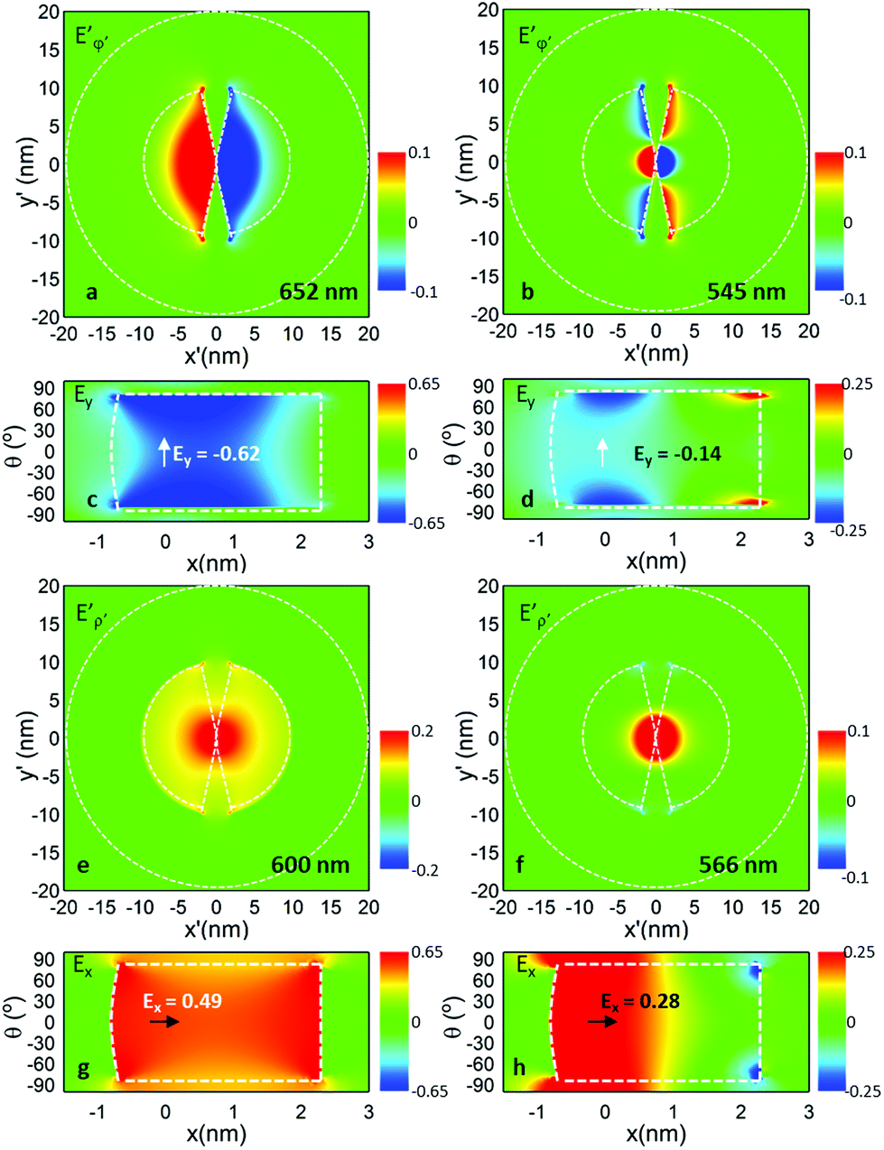
 has one antinode in between two nodes at the ends of the nanocavity (Fig. 4c), which corresponds to the first harmonic of the standing-wave pattern, i.e., the field distribution associated with the fundamental n = 1 LSP mode. For the second peak (Fig. 4d) Ey has two antinodes and three nodes, accounting for the second harmonic of the standing-wave pattern, i.e., the n = 2 LSP mode. For the horizontal emitter orientation, two Ex maxima are obtained at both ends with a node in between them at the first peak of
  (Fig. 4g), while the field distribution for the second peak (Fig. 4h) has a node in between a maximum and a minimum at the ends of the nanocavity.
 . For the vertical emitter orientation (Fig. 4a–d), the emitter [at (x′, y′) = (1, 0) in the real space, and (x, y) = (0, 0) in the transformed space] is located at a position where the field strength of the n = 1 LSP mode is larger (Ey = −0.62) than that of the n = 2 LSP mode (Ey = −0.14). The field integral overlap is therefore larger for n = 1, resulting in a higher
  (as shown in Fig. 3c). The same argument applies to the horizontal emitter orientation case (Fig. 4e–h).
 ,
,  is plotted against the emitter position along the x′ axis in Fig. 5c and d under vertical and horizontal emitter orientations, respectively. These analytical results are in agreement with numerical simulations depicted in Fig. 5e and f. The peak of
  related to the fundamental LSP is visible regardless of the emitter orientation and position, but its magnitude is enhanced for positions closer to the centre for vertical emitter orientation, whereas it is more constant for horizontal emitter orientation. Namely, for n = 1 LSP mode,
  is equal to 1.11 × 10⁶, 0.72 × 10³ and 9.5 × 10³ for vertical emitter orientation and 6.45 × 10⁴, 1.3 × 10³ and 1.6 × 10³ for horizontal emitter orientation at x′ = 0.3 nm, x′ = 6.6 nm and x′ = 9.6 nm, respectively. These gradient responses in
  for vertical and horizontal emitter orientations account for the strong and weak asymmetric field distributions of the n = 1 LSP mode in Fig. 4c and g, respectively, and also reflect the significant contribution of higher-order LSP modes for x′ → 0 and 10 nm; emitters placed close to metal boundaries (either by the nanocavity centre or by its outer periphery) couple more efficiently to the higher-order LSP modes that are accumulated at such boundaries (see the wavelength range below 600 nm in Fig. 4c–f).29,42 These additional non-radiative channels contribute to the total
  , yielding an overall increase of the
  baseline.
 for the bowtie nanocavity with θ′ = 20° and a vertical (c, e) and a horizontal emitter (d, f) at y′ = 0 and moving along the x′ axis. Numerical
  for vertical (g) and horizontal emitter orientations (h).
 within such an approximate wavelength range at both ends of the spatial window displayed (Fig. 5c–f).
 (calculated as the power radiated by the bowtie nanocavity, Pr, normalized to the power radiated by the emitter P0) as a function of the position of the emitter are shown in Fig. 5g and h for vertical and horizontal emitter orientations, respectively. These results show that
  is three orders of magnitude lower than
  , and thus, sustains the initial assumption of the theoretical frame that radiation losses are negligible in the system. From these results, one can also note that higher-order LSP modes have negligible radiative character compared to n = 1 LSP mode, since they are not dipolar in nature unlike the fundamental LSP mode.
 when the emitter moves along the y′ axis at x′ = 2.6 nm are shown in Fig. 6c and d along with the numerical results (Fig. 6e and f). As observed, the magnitude of the
  for the different LSP modes is enhanced when the emitter is close to the metal (as was shown when the emitter was moved along the x′ axis in Fig. 6c–f). For instance, for the LSP with n = 1, the
  is 8.95 × 10³ and 6.54 × 10⁴ for vertical emitter orientation and 4.22 × 10³ and 2.29 × 10⁴ for horizontal emitter orientation at y′ = 0 nm and y′ = 9.6 nm, respectively. Finally, the results of
  are shown in Fig. 6g and h with, again, values three orders of magnitude lower than
  , as in Fig. 5g and h.
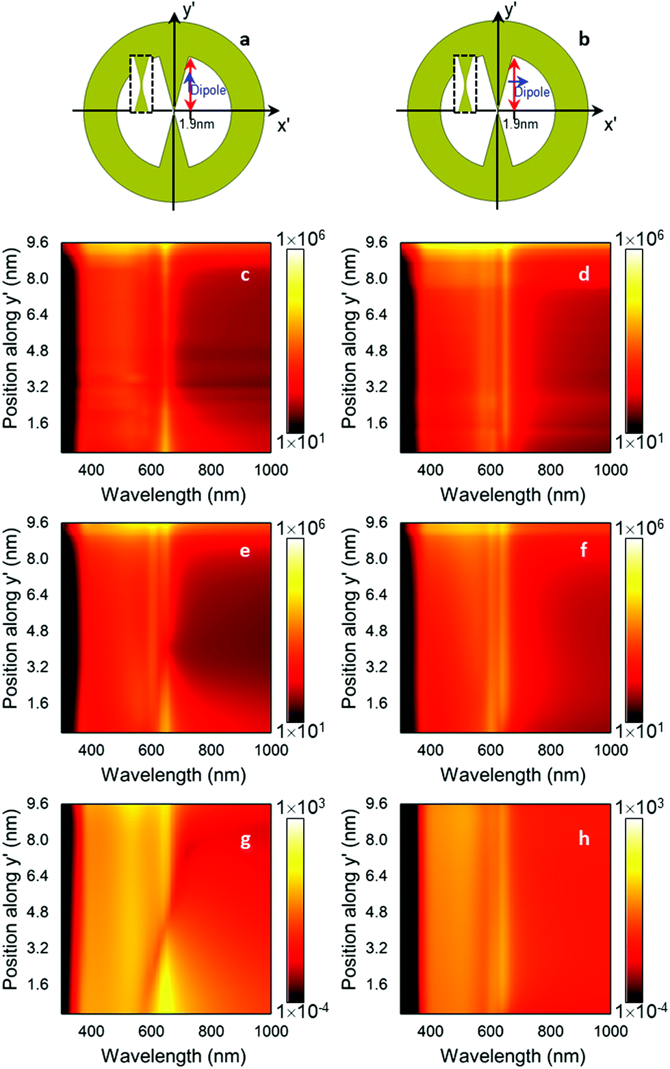
 for the bowtie nanocavity with θ′ = 20° and a vertical (c, e) and a horizontal emitter (d, f) at x′ = 2.6 nm and moving along the y′ axis. Numerical
  for vertical (g) and horizontal emitter orientations (h).
 . Given the aqueous environment, Brownian motion should be taken into account. Hence, the potential is normalized to kBT, where kB is the Boltzmann constant and T the temperature, which is taken to be 300 K.