3D computer-aided nanoprinting for solid-state nanopores†
Haibo
Ding
 ab,
Qiming
Zhang
a,
Zhongze
Gu
b and
Min
Gu
 *a
*a
aLaboratory of Artificial-Intelligence Nanophotonics, School of Science, RMIT University, Melbourne, VIC 3001, Australia. E-mail: min.gu@rmit.edu.au
bState Key Laboratory of Bioelectronics, School of Biological Science and Medical Engineering, Southeast University, Nanjing 210096, China
First published on 13th March 2018
Abstract
Here we report on the generation of solid-state nanopores with controllable sizes and shapes based on direct laser writing with a computer-aided two-photon polymerization process. Through a theoretical and experimental study of the accumulation effect during the two-photon polymerization, we have achieved nanopores with an inner diameter of down to ∼λ/10 (76.9 nm) for the first time, which is far beyond Abbe's diffraction limit. The generated nanopores can be stacked to form a channel with desired asymmetric shapes. This work provides the potential to integrate the solid-state nanopores into functional devices and opens up a new avenue for optimizing the gating properties of artificial membranes.
Conceptual insightsBio-inspired membranes based on solid-state nanopores have been widely studied over the past two decades. We propose a strategy to realize designable solid-state nanopores using two-photon polymerization for the first time. Numerical models have been developed to reveal the accumulation effects of exposure doses during the two-photon polymerization and to guide the fabrication of nanopores with complex geographic designs. Solid-state nanopores with subdiffraction openings and desired shapes have been successfully fabricated by controlling the laser power, scanning speed, and the fabrication path. The ability of two-photon polymerization to integrate nanopores into microstructures opens up the enormous potential applications for solid-state nanopores in artificial membranes and their derivative devices. |
A biological membrane in the human body is a selective barrier to fulfill the transport of ionic or molecular cargo.1,2 Pores embedded in the membrane can filter small molecules based on size and select specific molecules based on charge and other physicochemical properties.3,4 Inspired by biological models, artificial channel-based membranes have emerged as ideal candidates for mimicking the gating properties of the biological membranes and have been integrated into intelligent devices for different applications, such as DNA sequencing,5 biological sensing,6 and nanofluidic devices.7 In general, artificial channels can be classified into membrane nanopores and solid-state nanopores. Compared with membrane nanopores, which are self-assembled from proteins, peptides, synthetic organic compounds and even DNA,2 solid-state nanopores are fabricated by etching a hole into a solid film, using methods such as track-etching,8 focused-ion-beam etching,9 an electron-beam technique,10 and anodic oxidation.11 The solid materials show great advantages including high chemical and mechanical stability, controllable diameter and channel depth, and the potential for integration into devices and chips.1 The gating properties of artificial membranes based on solid materials depend on the size effect of the membrane pores. For nanopores with a size comparable to the thickness of the electrical double layer (smaller than 20 nm), the ion-current rectification due to the surface charge effect results in a preferential direction of the ion flow.12,13 A series of solid-state nanopores with symmetric and asymmetric shapes have demonstrated shape-dependent symmetric and asymmetric ion transport properties similar to those of biological ion channels.14,15 For pores with diameters ranging from 0.2 μm to 20 μm, the physical size of the opening and the capillary effect inside the channel can be applied to switch the membrane between its “off” and “on” states.16,17 Therefore, the generation of multiple complex shapes in one membrane becomes significant for the gating properties of artificial membranes based on solid porous structures.
Direct laser writing (DLW) based on two-photon polymerization has been widely used to fabricate complex microstructures due to its advantage in generating arbitrary three-dimensional geometrical configurations.18–21 Based on the point spread function of the focus spot, the polymerization structures could be calculated by the computer before fabrication.22,23 This direct fabrication method offers the potential to find the optimum structural shapes of solid porous structures that have the best gating properties and to integrate different channels into one platform.
Here, we report on the first fabrication of solid-state nanopores with controllable sizes and shapes by DLW. The laser power, fabrication speed and process path are considered in order to understand their effects on the polymerized size of the two-photon polymerization that in turn affects the fabrication quality of the nanopores. To push the narrow opening of the nanopores to the limit and to achieve a complex shape of the channels, we built theoretical models to investigate the influence that the relevant parameters have on the nanopores fabricated using the two-photon polymerization. Experiments were performed to verify the simulated predictions. Based on the theoretical model, nanopores with different shapes designed using computational methods can be printed by DLW. The diameter of the nanopores reached 76.9 nm, which is smaller than the diffraction limit barrier, and the interior shape of the channel could be adjusted by stacking along the vertical direction.
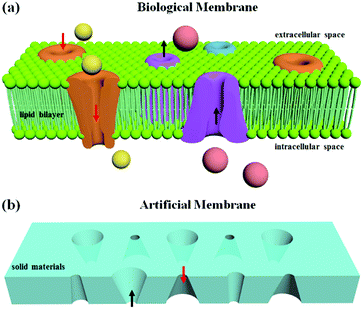
As illustrated in Fig. 1a, the ion channels for different ions and transport directions in biological membranes are not uniform in distribution and the structural shapes are asymmetric. Inspired by the biological model, an artificial membrane based on solid-state nanopores was generated in a solid film. The asymmetric shapes resulted in an ion-current rectification, enabling a preferential direction for the flow of ions. By using DLW, solid-state nanopores with different asymmetric shapes could be realized in the same film to satisfy the function of ion transport in two directions (Fig. 1b). As such, DLW allows ion channels to be located in specified locations and with specified shapes in the artificial membrane.
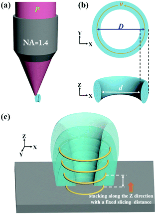
Theoretically, two-photon polymerization occurs within the focal volume of the objective when the exposure doses exceed a threshold value. Multiple focal spots along an appropriate fabrication path can result in a continuous structure with a coalescence of the polymerization. The photoresist has a memory effect for sub-threshold exposure due to the diffusion of the free radicals generated by the two-photon absorption.23,24 Due to the serial process of the DLW fabrication, extra polymerization is generated adjacent to the scanning path when the concentration of radicals is high enough to initiate the cross-linking of the polymers. Thus, the entire exposure doses which are proportional to the squared intensities can be calculated to predict the real size of the fabrication. By calculating the distribution of the exposure doses for single and multiple focus spots, a circular path in the XY plane produces a ring structure and the height of the ring structures can be increased by the accumulation of multiple layers in the Z direction (Fig. S1, ESI†). Based on simulation models, we designed a processing path for nanopores fabricated by DLW. The photoresist along the fabrication track would polymerize into the solid state while the unpolymerized photoresist in the central zone would be washed away after the development process, leaving a through pore (Fig. 2a). The processing path consists of a circular path in the XY plane (Fig. 2b) and a stacking of circular paths in the vertical direction with a fixed slicing distance to achieve a complete nanopore (Fig. 2c).
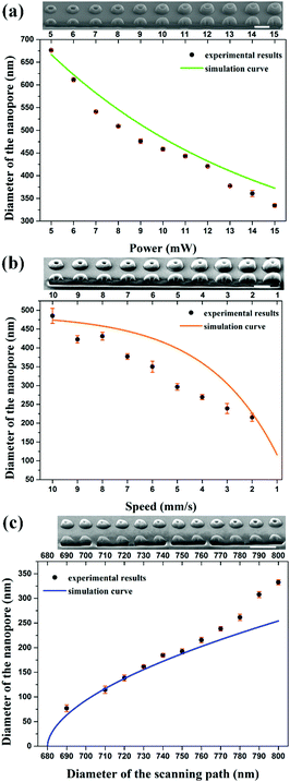
By calculating the distribution of the exposure doses within the fabrication area, we built a numerical model to investigate the influence of the related parameters, including the laser power (P), the scanning speed (v), and the diameter of the scanning path (D). The diameter of the nanopores (d) could be predicted according to a fixed threshold value (see “ESI†”). As shown in Fig. S2a and b (ESI†), the diameter of the nanopores is considered as the difference between the fixed diameter of the scanning path and the size of the polymerization voxel. With an increase in the laser power or a reduction in the scanning speed, the two-photon polymerization results in a larger voxel size,25 leading to a smaller diameter of the nanopores. However, a higher laser power would bring about uncontrollable thermal effects26 and a slower scanning speed would reduce the fabrication efficiency. It is necessary to change the diameter of the scanning path to control the diameter of the nanopores to avoid the use of a high laser power and slow scanning speed (Fig. S2c, ESI†). The relationship between the diameter of the scanning path and the corresponding diameter of the nanopore is nonlinear due to the extra polymerization which results from the accumulation effect of the exposure doses occurring in the central zone when reducing the diameter of the scanning path. Previous research has been performed to avoid such an accumulation effect with another inhibition beam and to realize subdiffraction gaps between features.27–29 In this work, we took advantage of the accumulation effect to generate a sub-100 nm opening and demonstrated that a subdiffraction pore can be realized without using an inhibition beam.
In order to confirm the simulation models, we fabricated three solid-state nanopore arrays using different laser powers, scanning speeds, and diameters of the scanning paths. Throughout this work, the slicing distance for fabrication in the axial direction was set at 300 nm (Fig. S3, ESI†). A commercial DLW system (Nanoscribe) was used for the fabrication. Femtosecond laser pulses with a wavelength of 780 nm were focused into the photoresist (IP-L 780, Nanoscribe) with an oil immersion objective (NA = 1.4, 63×). After fabrication, the structures were developed in a SU-8 developer for 5 minutes, rinsed in isopropyl alcohol, and finally dried with nitrogen gas. To measure the diameter of each nanopore, a focused ion beam milling process (FEI Scios Dualbeam FIBSEM) was performed to image the cross-sections. A 3 nm thick Pt layer was deposited on the surface to act as a conducting layer. The experimental results can be fitted with the prediction curve of the numerical simulation data (Fig. 3). A laser power of 10 mW and a scanning speed of 10 mm s−1 were chosen to fabricate the structures. The smallest nanopore achieved has a diameter of 76.9 nm, made by using a scanning path with a diameter of 690 nm, which is 1/10th of the beam wavelength. The fitting curve reveals the diameter dependence of the generated nanopores on the scanning path and indicates possible nanopores with a sub-50 nm diameter.
Due to the physical sizes of their pore openings, the nanopores generated by our method can act as filters to block objects with larger sizes. Other gating properties would be achieved by reducing the diameters to molecular dimensions or by modifying the inner walls of the pores with responsive materials. The opening of the solid-state nanopores could be decreased to a smaller diameter by depositing metals and metallic oxides including Au, Pt and TiO2 on the surface of the polymer structures. The thickness could be controlled to tens of nanometers by monitoring the deposition conditions.30 Besides this, the deposited layer provides a substrate surface upon which to modify functional molecules through chemical interactions.31 For example, poly(N-isopropylacrylamide) molecules with terminal thiol groups that have temperature-responsive properties could be attached onto a gold substrate through Au–thiol interactions.32
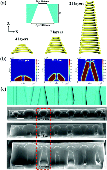
The gating properties of artificial membranes rely not only on the opening size but also the internal shape of the channel. Cylindrical, conical, cigar-like, and hour-glass shapes have demonstrated their abilities in different gating strategies.31 DLW provides the ability to generate arbitrary geometrical configuration, thus we could fabricate nanopores with different shapes. For a nanopore with a conical shape, as shown in Fig. 4a, the diameters for the scanning path were designed as 800 nm for the narrow opening and 2400 nm for the large opening. The slope of the conical shape was controlled by the height of the nanopore and the number of stacking layers. For a fixed slicing distance of 300 nm, the number of stacking layers was 4, 7, and 21 for heights of 1 μm, 2 μm, and 6 μm. The numerical simulations indicated that the axial elongation of the polymerized voxel (1 μm) and the accumulation effect of the exposure doses in the Z direction contributed to the thickness of the nanopore walls (Fig. 4b). Asymmetric shapes can be achieved by designing a height of larger than 1 μm. Geometric designs for the solid-state nanopores with typical cylindrical, conical, cigar-like, and hour-glass shapes were carried out (Fig. S4 and Table S1, ESI†). Fig. 4c shows the schematic designs and the resulting structures with heights of 1 μm, 2 μm, and 6 μm. The fabricated nanopores with a height of 6 μm maintained the same shape as that in the original design, which was in agreement with the simulation results, shown in Fig. 4b.
Moreover, DLW offers the possibility of integrating these nanopores into microstructures. Using these optimized fabrication conditions with a laser power of 10 mW, a scanning speed of 10 mm s−1 and a slicing distance of 300 nm, we successfully fabricated an array of pillars, an array of cubes, and a film with nanopores embedded in them (Fig. 5). The position and individual shape of each nanopore could be controlled by the geometric design of the processing path.
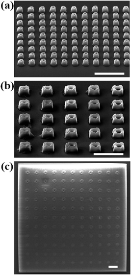 | ||
| Fig. 5 SEM images of microstructures with nanopores fabricated by DLW. (a) An array of pillars; (b) an array of cubes; (c) a film. Scale bar, 5 μm. | ||
Conclusions
In conclusion, we have investigated the influence of the laser power, scanning speed, fabrication path, and slicing distance on the DLW fabrication of solid-state nanopores. Numerical models have been developed to reveal the accumulation effects of the exposure doses and to guide the fabrication of nanopores with complex geographic designs. Using the accumulation effect, we have achieved nanopores with an inner diameter of down to 76.9 nm (∼λ/10, which is below the diffraction limit) and with typical asymmetric shapes. To satisfy the ion transport function for solid-state nanopores, super-resolution DLW33–36 could be applied to reduce the nanopore opening down to sub-50 nm and maybe even down to sub-10 nm in the future. We believe that the DLW method will promote the research of bio-inspired membranes based on solid-state nanopores and realize functional devices with integrated nanopore structures.Conflicts of interest
The authors declare no competing financial interests.Acknowledgements
M. G. acknowledges support from the Australian Research Council for its support through the Discovery Projects (DP170101775). Z. G. and H. D. acknowledge the National Natural Science Foundation of China (Grants 21327902 and 21635001). As a joint PhD student, H. D. was also partially supported by a fellowship from the China Scholarship Council. The authors acknowledge the facilities, and the scientific and technical assistance, of the Australian Microscopy & Microanalysis Research Facility at RMIT University.Notes and references
- C. Dekker, Nat. Nanotechnol., 2007, 2, 209–215 CrossRef CAS PubMed.
- S. Howorka, Nat. Nanotechnol., 2017, 12, 619–630 CrossRef CAS PubMed.
- E. Gouaux and R. MacKinnon, Science, 2005, 310, 1461–1465 CrossRef CAS PubMed.
- D. C. Gadsby, Nat. Rev. Mol. Cell Biol., 2009, 10, 344–352 CrossRef CAS PubMed.
- E. A. Manrao, I. M. Derrington, A. H. Laszlo, K. W. Langford, M. K. Hopper, N. Gillgren, M. Pavlenok, M. Niederweis and J. H. Gundlach, Nat. Biotechnol., 2012, 30, 349–353 CrossRef CAS PubMed.
- S. Howorka and Z. Siwy, Chem. Soc. Rev., 2009, 38, 2360–2384 RSC.
- H. Craighead, Nature, 2006, 442, 387–396 CrossRef CAS PubMed.
- P. Apel, Radiat. Meas., 2001, 34, 559–566 CrossRef CAS.
- J. Li, D. Stein, C. McMullan, D. Branton, M. J. Aziz and J. A. Golovchenko, Nature, 2001, 412, 166–169 CrossRef CAS PubMed.
- A. J. Storm, J. H. Chen, X. S. Ling, H. W. Zandbergen and C. Dekker, Nat. Mater., 2003, 2, 537–540 CrossRef CAS PubMed.
- W. Lee, K. Schwirn, M. Steinhart, E. Pippel, R. Scholz and U. Gösele, Nat. Nanotechnol., 2008, 3, 234–239 CrossRef CAS PubMed.
- Z. S. Siwy, Adv. Funct. Mater., 2006, 16, 735–746 CrossRef CAS.
- G. Pérez-Mitta, L. Burr, J. S. Tuninetti, C. Trautmann, M. E. Toimil-Molares and O. Azzaroni, Nanoscale, 2016, 8, 1470–1478 RSC.
- E. B. Kalman, I. Vlassiouk and Z. S. Siwy, Adv. Mater., 2008, 20, 293–297 CrossRef CAS.
- H. Zhang, Y. Tian, J. Hou, X. Hou, G. Hou, R. Ou, H. Wang and L. Jiang, ACS Nano, 2015, 9, 12264–12273 CrossRef CAS PubMed.
- X. Hou, Y. Hu, A. Grinthal, M. Khan and J. Aizenberg, Nature, 2015, 519, 70–73 CrossRef CAS PubMed.
- X. Hou, Adv. Mater., 2016, 28, 7049–7064 CrossRef CAS PubMed.
- S. Kawata, H. B. Sun, T. Tanaka and K. Takada, Nature, 2001, 412, 697–698 CrossRef CAS PubMed.
- M. Deubel, G. von Freymann, M. Wegener, S. Pereira, K. Busch and C. M. Soukoulis, Nat. Mater., 2004, 3, 444–447 CrossRef CAS PubMed.
- S. Maruo and J. t. Fourkas, Laser Photonics Rev., 2008, 2, 100–111 CrossRef CAS.
- T. Gissibl, S. Thiele, A. Herkommer and H. Giessen, Nat. Photonics, 2016, 10, 554–560 CrossRef CAS.
- M. D. Turner, M. Saba, Q. Zhang, B. P. Cumming, G. E. Schröder-Turk and M. Gu, Nat. Photonics, 2013, 7, 801–805 CrossRef CAS.
- J. Fischer and M. Wegener, Laser Photonics Rev., 2013, 7, 22–44 CrossRef CAS.
- I. Sakellari, E. Kabouraki, D. Gray, V. Purlys, C. Fotakis, A. Pikulin, N. Bityurin, M. Vamvakaki and M. Farsari, ACS Nano, 2012, 6, 2302–2311 CrossRef CAS PubMed.
- H. B. Sun, K. Takada, M. S. Kim, K. S. Lee and S. Kawata, Appl. Phys. Lett., 2003, 83, 1104–1106 CrossRef CAS.
- C. N. LaFratta, J. T. Fourkas, T. Baldacchini and R. A. Farrer, Angew. Chem., Int. Ed., 2007, 46, 6238–6258 CrossRef CAS PubMed.
- J. Fischer and M. Wegener, Opt. Mater. Express, 2011, 1, 614–624 CrossRef CAS.
- R. Wollhofen, J. Katzmann, C. Hrelescu, J. Jacak and T. A. Klar, Opt. Express, 2013, 21, 10831–10840 CrossRef CAS PubMed.
- Z. Gan, M. D. Turner and M. Gu, Sci. Adv., 2016, 2, e1600084 Search PubMed.
- M. Nishizawa, V. P. Menon and C. R. Martin, Science, 1995, 268, 700–702 CrossRef CAS PubMed.
- X. Hou, H. Zhang and L. Jiang, Angew. Chem., Int. Ed., 2012, 51, 5296–5307 CrossRef CAS PubMed.
- W. Guo, H. Xia, F. Xia, X. Hou, L. Cao, L. Wang, J. Xue, G. Zhang, Y. Song, D. Zhu, Y. Wang and L. Jiang, ChemPhysChem, 2010, 11, 859–864 CrossRef CAS PubMed.
- L. Li, R. R. Gattass, E. Gershgoren, H. Hwang and J. T. Fourkas, Science, 2009, 324, 910–913 CrossRef CAS PubMed.
- E. Nicoletti, D. Bulla, B. Luther-Davies and M. Gu, Nano Lett., 2011, 11, 4218–4221 CrossRef CAS PubMed.
- Z. Gan, Y. Cao, R. A. Evans and M. Gu, Nat. Commun., 2013, 4, 2061 Search PubMed.
- J. Fischer, J. B. Mueller, A. S. Quick, J. Kaschke, C. Barner-Kowollik and M. Wegener, Adv. Opt. Mater., 2015, 3, 221–232 CrossRef CAS.
Footnote |
| † Electronic supplementary information (ESI) available. See DOI: 10.1039/c8nh00006a |
| This journal is © The Royal Society of Chemistry 2018 |

