
Group 6 transition metal dichalcogenide nanomaterials: synthesis, applications and future perspectives
Morasae
Samadi†
 a,
Navid
Sarikhani†
b,
Mohammad
Zirak
a,
Hua
Zhang
*c,
Hao-Li
Zhang
*d and
Alireza Z.
Moshfegh
*ae
a,
Navid
Sarikhani†
b,
Mohammad
Zirak
a,
Hua
Zhang
*c,
Hao-Li
Zhang
*d and
Alireza Z.
Moshfegh
*ae
aDepartment of Physics, Sharif University of Technology, Tehran 11155-9161, Iran. E-mail: moshfegh@sharif.edu
bSchool of Mechanical Engineering, Sharif University of Technology, Tehran 11155-9567, Iran
cCenter for Programmable Materials, School of Materials Science and Engineering, Nanyang Technological University, 50 Nanyang Avenue, Singapore 639798, Singapore. E-mail: hzhang@ntu.edu.sg
dState Key Laboratory of Applied Organic Chemistry, College of Chemistry and Chemical Engineering, Lanzhou University, Lanzhou 730000, P. R. China. E-mail: haoli.zhang@lzu.edu.cn
eInstitute for Nanoscience and Nanotechnology, Sharif University of Technology, Tehran 14588-8969, Iran
First published on 4th December 2017
Abstract
Group 6 transition metal dichalcogenides (G6-TMDs), most notably MoS2, MoSe2, MoTe2, WS2 and WSe2, constitute an important class of materials with a layered crystal structure. Various types of G6-TMD nanomaterials, such as nanosheets, nanotubes and quantum dot nano-objects and flower-like nanostructures, have been synthesized. High thermodynamic stability under ambient conditions, even in atomically thin form, made nanosheets of these inorganic semiconductors a valuable asset in the existing library of two-dimensional (2D) materials, along with the well-known semimetallic graphene and insulating hexagonal boron nitride. G6-TMDs generally possess an appropriate bandgap (1–2 eV) which is tunable by size and dimensionality and changes from indirect to direct in monolayer nanosheets, intriguing for (opto)electronic, sensing, and solar energy harvesting applications. Moreover, rich intercalation chemistry and abundance of catalytically active edge sites make them promising for fabrication of novel energy storage devices and advanced catalysts. In this review, we provide an overview on all aspects of the basic science, physicochemical properties and characterization techniques as well as all existing production methods and applications of G6-TMD nanomaterials in a comprehensive yet concise treatment. Particular emphasis is placed on establishing a linkage between the features of production methods and the specific needs of rapidly growing applications of G6-TMDs to develop a production-application selection guide. Based on this selection guide, a framework is suggested for future research on how to bridge existing knowledge gaps and improve current production methods towards technological application of G6-TMD nanomaterials.
 Morasae Samadi | Morasae Samadi obtained her BSc and MSc in organic chemistry from Sharif University of Technology (SUT), Iran, in 2005 and 2007, respectively. She received her PhD in Nanomaterials from SUT in 2013. Afterwards, she joined the Nano, Energy, Surface and Thin films (NEST) group as a postdoctoral researcher to study 2D layered materials. Her current research interests focus on the synthesis of 2D nanomaterials to understand their photochemistry for applications in water remediation and clean energy. |
 Navid Sarikhani | Navid Sarikhani is currently a PhD student of mechanical engineering at Sharif University of Technology, Iran. He received BSc and MSc degrees in the same discipline and has had a long journey from engineering to physics and nanoscience. His primary research interest is superconductivity—the quest for perfection in a regular incomplete environment and the pursuit of an ideal in a real world. Navid enjoys physics, mathematics and philosophy of science as well as computer art design, scriptures and poems. |
 Mohammad Zirak | Mohammad Zirak obtained his PhD (2016) and MSc (2010) degrees in nano-physics from Sharif University of Technology of Iran, under the supervision of Prof. Alireza Z. Moshfegh. He joined Prof. Hao-Li Zhang's group at Lanzhou University of China in 2014 to work on two dimensional nanocrystals. Currently, he is an assistant professor of condensed matter physics at Hakim Sabzevari University, Iran. His research interests involve two dimensional materials, nano-photocatalysts, nanomaterials for solar energy conversion and environmental applications. |
 Hua Zhang | Hua Zhang obtained his BS (1992) and MSc (1995) degrees from Nanjing University, and completed his PhD with Prof. Zhongfan Liu at Peking University in 1998. As a Postdoctoral Fellow, he joined Prof. Frans C. De Schryver's group at Katholieke Universiteit Leuven (Belgium) in 1999, and then moved to Prof. Chad A. Mirkin's group at Northwestern University in 2001. After that he worked at NanoInk Inc. (USA) and Institute of Bioengineering and Nanotechnology (Singapore), and he joined Nanyang Technological University in 2006. His current research interests focus on the synthesis of ultrathin two-dimensional nanomaterials, semiconducting nanomaterials, and complex heterostructures. |
 Hao-Li Zhang | Hao-Li Zhang received his PhD from Lanzhou University in 1999. He then worked as postdoc in the University of Leeds and Oxford University. Since 2004, he has been appointed as a full professor by the State Key Laboratory of Applied Organic Chemistry (SKLAOC) of Lanzhou University. He is currently the deputy director of the SKLAOC and deputy dean of the College of Chemistry. In 2014, he was elected as a Fellow of the Royal Society of Chemistry, and was appointed as an Adjunct Professor at the University of Alabama. Prof. Zhang is interested in developing new functional materials for optoelectronic applications. |
 Alireza Z. Moshfegh | Alireza Z. Moshfegh received his PhD in Physics from the University of Houston (USA) in 1990. After two years postdoc work at Texas Center for Superconductivity at the University of Houston, he joined the Physics Department of Sharif University of Technology (SUT) in Tehran, Iran. He became a full professor in Physics in 2005 and then was elected as the chairman of the Physics Department at SUT from 2006 to 2009. His current research interests focus on the synthesis and characterization of low-dimensional materials in particular novel 2D transition metal dichalcogenides for clean energy and environmental applications. |
1. Introduction
In recent years, we have witnessed a resurgence of interest in a rather long-known and well-studied class of materials, called group 6 transition metal dichalcogenides (G6-TMDs), including most notably MoS2, MoSe2, MoTe2, WS2 and WSe2. A class sharing less than 100 papers per year in the scientific community before 2010, mainly as dry lubricants and hydrodesulfurization catalysts, today has become a booming research field ranging from (opto)electronics to sensors, energy storage and catalysis with above 3000 yearly published papers and several patents being filed monthly.Historically, G6-TMDs (in particular MoS2 and WS2), as inorganic analogues of graphite, have followed the footsteps of carbon nanomaterials and achieved most of their advancement and success, although usually with some delay. The discovery of carbon fullerenes by Smalley and coworkers1 in 1985 and carbon nanotubes by Iijima2 in 1991 was followed by the discovery of WS2 and MoS2 fullerenes and nanotubes between 1992 and 1995.3–5 Thus it was quite natural that the original report of discovery of graphene, a two-dimensional (2D) carbon crystal, by Novoselov, Geim and colleagues6 in 2004, was immediately followed by some preliminary experiments on TMDs such as MoS2.7 However, it took about seven years for G6-TMDs to step out of the shadow of the famous graphene and establish their own identity. Current intensive research on G6-TMDs has been stimulated by a series of follow-up theoretical predictions and experimental observations of unexpected electronic and optical properties in nanosheets of this family of materials, especially their most representative member, MoS2.
In 2010, Mak et al.8 kindled the first sparks by reporting the tunable bandgap in MoS2 nanosheets with respect to the thickness of nanosheets. More surprisingly, they found a transition from an indirect bandgap of 1.3 eV in bulk MoS2 to a very technologically favorable direct bandgap of 1.9 eV when MoS2 was thinned down to a single molecular layer. Direct bandgap means stronger light emission and higher luminescence quantum efficiency of MoS2 monolayer nanosheets, which is intriguing for fabrication of novel light emitting diodes, solar cells and photodetectors. A subsequent report on a single-layer MoS2 transistor with a high electron mobility and superior on/off current ratio by Kis and coworkers,9 in 2011, definitely ignited the field. These findings propelled accumulated efforts of researchers, who struggled with semimetallic zero-bandgap graphene to a newly rediscovered 2D semiconductor, a MoS2 nanosheet, and its other family members, such as WSe2 and MoTe2. In fact, the MoS2 nanosheet the builders rejected in 2004, due to its low electron mobility, has become a cornerstone. Although there was some systematic overestimation in the reported high electron mobilities of MoS2 transistors by Kis’ group in 2011 (see Section 6.1. (opto)electronics), a new hope appeared that was pursued with great enthusiasm and soon after yielded many fruitful results. Over the past 6 to 7 years, the basic science, characterization techniques and production methods of the whole family of G6-TMDs have been updated and revised, leading to many novel scientific and technological advancements. Such rapid progress even has shifted paradigms of traditional applications of G6-TMDs, such as lubrication and catalysis, because several novel and efficient production methods have been emerged and a better understanding has been gained in recent years.
G6-TMDs are members of a broader family of materials called transition metal chalcogenides (TMCs). According to the definition recommended by IUPAC (International Union of Pure and Applied Chemistry), a transition element or a transition metal (since they are all metals) is an element that has incomplete d sub-shells as a free atom or a commonly occurring cation.10,11 Based on this definition, groups 4 to 10 on the periodic table as well as some elements of groups 3 and 11 can be regarded as transition metals (Fig. 1).12 Chalcogen is also the generic name of the elements in group 16 of the periodic table, which comprises O, S, Se, Te and the two radioactive elements Po and Lv.12,13 Transition metal dichalcogenides (TMDs) constitute a large and important family of TMCs with the generalized formula of MX2, where M is a transition metal and X is a chalcogen.14,15 TMDs have been known and studied for decades and cover a wide range of electronic properties from insulators (HfS2 and ZnS2), through semiconductors (MoS2 and ReS2) and semimetals (WTe2, NbTe2), to true metals (NbS2 and CoTe2).14 Over 60 transition metal dichalcogenides are known and about 40 of them have layered crystal structure, which are predominantly TMDs of groups 4 to 7.14,16 Among these layered TMDs, the group 6 transition metal dichalcogenides (G6-TMDs) are of special scientific and technological importance. MoS2, the most representative compound of G6-TMDs, is an earth abundant material, which has been known for several centuries. Its dry lubricant properties,17 catalytic activity18 and intercalation chemistry19 were extensively studied in the 1960s and 1970s.
 | ||
| Fig. 1 Constituent elements of Group 6 Transition Metal Dichalcogenides (G6-TMDs) highlighted and embossed in the periodic table along with three conventional systems of group numbering. Five semiconducting compounds, MoS2, MoSe2, MoTe2, WS2 and WSe2, are in the focus of this review. Note that WTe2 is a semimetal and hence not discussed much. Chromium and oxygen generally form compounds with stoichiometries other than dichalcogenides, such as Cr2S3 and MoO3, and thus their related compounds are not the primary focus here. Sg, Po and Lv are also radioactive elements and their related compounds are excluded from our discussion. Representation format of the periodic table and details such as elements belonging to group 3 are adopted from ref. 20 and 21. | ||
In this review, we focus on group 6 transition metal dichalcogenides, which will be abbreviated as G6-TMDs to be consistent with previously suggested acronyms.22 The main emphasis, as highlighted in Fig. 1, is on five semiconducting layered compounds including MoS2, MoSe2, MoTe2, WS2 and WSe2 with technologically appropriate bandgaps of 1 to 2 eV. WTe2, another important compound of this group, is a semimetal. Large magnetoresistance (change of electrical resistivity with an applied magnetic field), a rare and exotic property of limited materials, has been reported for WTe2, recently.23 WTe2 is also a hot topic in condensed matter physics as a new type of Weyl semimetal, the 3D topological analogues of 2D graphene with massless relativistic electrons.24 However, we focus here on semiconducting G6-TMDs and WTe2 is excluded from our discussion. Chromium chalcogenides also are not covered here, since the most stable oxidation state of chromium is Cr(III) and while compounds with low oxidation states, such as CrS and Cr2S3 are stable, chromium dichalcogenides, in which chromium is present as Cr(IV), are unstable.25 Nevertheless, a brief discussion is given in Section 5.3., Intercalation and exfoliation, on the stabilization of chromium dichalcogenides upon intercalation in ternary stoichiometric phases, such as NaCrS2 and KCrS2.26 The situation for oxygen is the same and certain stoichiometries other than dioxides, especially trioxides (e.g. MoO3 and WO3), are more stable.12 For a through and up-to-date treatment of molybdenum trioxide, a review article by Kalantar-Zadeh and coworkers is suggested.27 The radioactive elements seaborgium (Sg), polonium (Po) and livermorium (Lv) and their related compounds are also excluded from our discussion.
There are some high quality reviews on the synthesis, properties, and applications of TMD nanomaterials, particularly G6-TMDs. Tenne and Redlich28 reviewed inorganic nanotubes and fullerene-like nanoparticles, including G6-TMDs, several years ago. A highly insightful review by Chhowalla and colleagues15 provides a unique in-depth discussion of the chemistry of TMD nanosheets with a balanced view of their important production methods and cutting-edge applications. Another highly pertinent tutorial review by Zhang's group29 gives an accurate overview of nearly all aspects of the TMD nanosheet research field. This particular article focused on four different production methods namely, mechanical cleavage, electrochemical lithium intercalation–exfoliation, sonication and chemical vapour deposition (CVD) and covered (opto)electronics, sensing and energy storage applications. Chen's group30 also contributed a comprehensive article on graphene-like two-dimensional materials, including G6-TMDs, and discussed a number of well-established methods for producing these materials. Recently, after the first stage of research and development, at the dawn of technological applications of TMDs, a new trend of application-oriented review articles and themed issues of journals has been emerging.15,31 For example, Liu's group32 has provided a detailed discussion on CVD growth of G6-TMD monolayers and outlined the future fine-tuning pathways for these nanosheets so as to be used in highly-demanded nano/opto-electronics and photocatalytic applications. Applications of G6-TMDs in transistor electronics,33,34 sensing,35,36 photocatalysis,37 water splitting38 and nanomedicine39 have also been reviewed, recently.
Fig. 2 illustrates the approach and the key differentiating aspects of our review. To fulfil the needs of many existing and potential technological applications, we aim to compile and to consolidate information on science and production of all G6-TMD nanomaterials in a cognitive framework appealing to scientists and engineers of various disciplines. While our emphasis is on 2D nanosheets, we also review other nanomaterials of this group such as, 0D quantum dots, 1D nanotubes and 3D nanoflowers. For this purpose, based on Web of Science, a database of more than 4500 highly cited articles in high-impact journals with carefully chosen keywords to cover all G6-TMD nanomaterials from 2004 to 2017 has been prepared and thoroughly studied. In the first four sections, a practical review of the basic science and structural, electronic and optical properties of G6-TMDs as well as their characterization toolbox is provided. Then a systematic classification of all different existing production methods of various nanomaterials of G6-TMDs is presented. Although there are a number of review articles on some specific production methods of 2D TMD nanosheets,32,40–42 a comprehensive treatment of science and all production methods of all G6-TMD nanomaterials is necessary and still lacking. In this respect, all production methods are first categorized into top-down and bottom-up approaches. Then, top-down methods are divided into four main subcategories including (i) mechanical cleavage, (ii) liquid phase exfoliation, (iii) intercalation and exfoliation and (iv) thinning. Bottom-up methods are also divided into two main subcategories of (i) vapour deposition and (ii) solution-based synthesis (Fig. 2). Finally, these six main subcategories are further segmented into 18 distinct types of production methods and are discussed in detail. Some of these production methods, such as thermal annealing, etching, sputter deposition and pulsed laser deposition, are often overlooked by researchers, while, as will be discussed later, these methods have great potential and promise for numerous advanced device applications.
 | ||
| Fig. 2 Looking at the science and various production methods of group 6 transition metal dichalcogenide (G6-TMD) nanomaterials from the viewpoint of technological applications. The figure illustrates the necessity of establishing a linkage between the features of production methods and the specific needs of rapidly growing applications of G6-TMDs. Data in the figure are extracted and compiled from a database of top 1000 most cited articles with any of the G6-TMD nanomaterials in their topic based on Web of Science. | ||
We also categorize all reported applications of G6-TMD nanomaterials into five main areas, based on the structural and functional features of the nanomaterials needed by each application. The pertinent subsections, as indicated in Fig. 2, are (i) (opto)electronics, (ii) sensors, (iii) energy storage, (iv) catalysis and (v) emerging applications. Each subsection is organized in a way so that first the basic concepts are briefly introduced. Then, potential and utilized production methods for the mentioned applications in that subsection are discussed and the current challenges are critically analysed to outline the possible solutions and pathways for future research. More importantly, in this section we present a production-application selection guide in order to provide insight into the fundamental question of “which production method is suitable for which application?”. This selection guide is intended to address the needs of those specialists seeking for better alternative production methods for their specific application or possible new applications of their produced nanomaterials, without going through all details of the article.
In the last section, conclusions arising from our literature review are summarized and a framework is suggested for important and high-priority research topics in the field of G6-TMD nanomaterials. From the fundamental science perspective, unclear problems and open questions along with unexplored areas and phenomena are addressed. Steps that should be taken to improve existing production methods and the possibility of combining multiple methods to exploit their complementary advantages are also discussed.
Finally, we would like to note that our review article is intended not to serve as an additional exhaustive data-gathering and cumbersome listing of references, but rather to provide an overview in a balanced and homogenized style on the field of G6-TMDs in a comprehensive yet concise treatment. The main objectives of our review are: (i) to portray the current science of G6-TMD nanomaterials from an application-oriented point of view; (ii) to provide readers with a working knowledge of all production methods through a critical and comparative presentation approach; (iii) to stimulate exchange of ideas between researchers working on different types of production methods; (iv) to outline the main targets and future research directions that should be pursued to improve existing production methods and develop new methods; (v) to draw attention of researchers to the wide available range of production methods for existing/emerging applications beyond the routine methods. In accordance with the purpose of the reader, the article can be used selectively and flexibly. Those readers that are intimately familiar with the subject may not need to read the article sequentially from beginning to end. Instead, they can start with the first two pages of Section 6 (Production-Application selection guide) and after checking Table 8, then continue with their desired topics, from the basic science and characterization methods to specific production methods and applications. Those specialists and advanced readers who are primarily looking for new thinking and novel ideas, will find Section 7 (Conclusion and outlook) particularly interesting and useful. It is sincerely hoped that this comprehensive review article will become a major reference work on group 6 transition metal dichalcogenides for many years. Therefore, a special emphasis is placed on using a consistent notation, terminology and abbreviations throughout the text in an effort to standardize definitions and nomenclatures of this multidisciplinary field.
2. Classification of nanomaterials by dimensionality
Group 6 transition metal dichalcogenide nanomaterials are very rich in morphology with various shapes, sizes, phases and surface topographies (Fig. 3). Each morphology possesses novel physical and chemical properties of its own, different from the bulk form, with generally high tunability and controllability of these properties. This variety of morphologies has a great promise from the application point of view and hence a systematic classification and organization of existing G6-TMD nanomaterials in a rational hierarchy would certainly be beneficial to researchers from both academia and industry to better utilize the accumulated knowledge of such a large library of nanomaterials. | ||
| Fig. 3 A catalog of some selected nano-objects and nanostructures of group-6 transition metal dichalcogenides, categorized according to ISO/TS 80004 (nanotechnologies-vocabulary). Reproduced with permission from, 0D nano-objects (nanoparticles): 0D-(i) ref. 46. Copyright 2015 Wiley-VCH; 0D-(ii) ref. 47. Copyright 2015 Wiley-VCH; 0D-(iii) ref. 48. Copyright 2005 Wiley-VCH; 0D-(iv) ref. 49. Copyright 2001 Elsevier B.V.; 0D-(v) ref. 50. Copyright 2004 American Chemical Society; 1D nano-objects (nanofibres): 1D-(i) ref. 51. Copyright 2000 American Chemical Society; 1D-(ii) ref. 52. Copyright 2006 Nature Publishing Group; 1D-(iii) ref. 53. Copyright 2010 The Royal Society of Chemistry; 1D-(iv) ref. 54. Copyright 2012 Elsevier B.V.; 1D-(v) ref. 55. Copyright 2013 American Chemical Society; 2D nano-objects (nanoplates): 2D-(i) ref. 56. Copyright 2013 American Chemical Society; 2D-(ii) ref. 57. Copyright 2014 Wiley-VCH; 2D-(iii) ref. 58. Copyright 2014 Nature Publishing Group; 2D-(iv) ref. 59. Copyright 2017 IOP Publishing Ltd; 2D-(v) ref. 60. Copyright 2013 American Chemical Society; 2D-(vi) ref. 61. Copyright 2014 The Royal Society of Chemistry; 2D-(vii) ref. 62. Copyright 2013 American Chemical Society; 2D-(viii) ref. 63. Copyright 2014 Wiley-VCH; 2D-(ix) ref. 64. Copyright 2013 Wiley-VCH; 3D nanostructures: 3D-(i) ref. 65. Copyright 2004 Wiley-VCH; 3D-(ii) ref. 66. Copyright 2015 The Royal Society of Chemistry; 3D-(iii) ref. 67. Copyright 2014 Elsevier B.V.; 3D-(iv) ref. 68. Copyright 2015 Elsevier B.V.; 3D-(v) ref. 69. Copyright 2014 The Royal Society of Chemistry; 3D-(vi) ref. 70. Copyright 2014 American Chemical Society; 3D-(vii) ref. 71. Copyright 2015 American Chemical Society; 3D-(viii) ref. 72. Copyright 2013 Wiley-VCH; 3D-(ix) ref. 73. Copyright 2015 The Royal Society of Chemistry. | ||
Classification of nanomaterials can be made based on several criteria such as composition, phase, crystal structure and dimensionality as well as electrical, magnetic, optical, thermal and chemical properties.43 A classifying system, named “nano-tree”, has been developed in this regard under the ISO/TR 11360 Nanotechnologies—methodology for the classification and categorization of nanomaterials. Among possible classifying systems, the one based on dimensionality is the most versatile and ubiquitous due to the inherent relationship between dimensionality and various physical and chemical properties, which makes this system more useful for qualitative prediction of the properties of each category. However, classification of nanomaterials based on dimensionality is challenging due to some considerations. For example, (i) what is the exact size below which a material can be considered a nanomaterial? (ii) Which lengths in material should be considered as characteristic lengths, especially for irregular shapes? (iii) Is observation of quantum size effects a necessary condition for nanomaterials? (iv) Which dimensions of nanomaterial should be considered in the classification, only external dimensions or internal dimensions of constituent fine structures? The last point may cause confusion when for instance a composite of nanoparticles and nanotubes in a bulk matrix needs to be categorized.
Gleiter44 was the first one who attempted to systematically classify nanomaterials; however, his classification was based on chemical composition and thermodynamic equilibrium state rather than dimensionality and thus, there were some limitations in the classification, for example, important nanomaterial categories such as fullerene and nanotubes were not taken into account. Pokropivny and Skorokhod45 extended the work of Gleiter by developing a system of numbering and coding of nanomaterials considering both external dimensions as a whole (k) and dimensionality of each individual constituent unit (l, m, n, …) in a typical kDlmn… designation. In addition, they tabulated 36 main classes of possible nanostructures and described their expected properties. Recently, two technical committees of ISO/TC 229 and IEC/TC 113 have been collaborating to develop a series of standards under the general title of ISO/TS 80004 Nanotechnology—vocabulary in order to unify the nanotechnology related vocabularies and terminology. According to this standard, the length range of 1 nm to 100 nm is called the nanoscale and a material with any external or internal dimension or surface structure at the nanoscale is called a nanomaterial. Nanomaterials are then classified into two main categories of (i) nano-objects, with at least one external dimension at the nanoscale and (ii) nanostructured materials, with external dimensions typically larger than the nanoscale but internal structures at the nanoscale. A nano-object itself is divided into three main categories of (i) nanoparticles, with all external dimensions at the nanoscale, (ii) nanofibres, with at least two external dimensions at the nanoscale and another dimension significantly (more than 3 times) larger than the other two, and (iii) nanoplates, with at least one dimension at the nanoscale and another two dimensions significantly larger.
Various nanoparticles of G6-TMDs have been synthesized, such as quantum dots, fullerenes, hollow polyhedral closed-cage structures and nanooctahedra (top-left panel in Fig. 3). According to ISO/TS 80004-2, a nanoparticle is referred to any nanomaterial with all three external dimensions below 100 nm. While nanoparticles fully realize benefits of spatial nano-sized dimensions and nano-size effects, such as high surface to volume ratio and size-dependent properties, they do not necessarily exploit remarkable quantum phenomena that require much more shrinkage in size. Quantum phenomena, including quantization of the energy spectrum and electron density of states as well as a substantial increase in bandgap and light absorption/emission, introduce another methodology for the classification of nanomaterials, which is the subject of ISO/TS 80004-12.
Based on the standard definition, nanomaterials are classified into quantum wells (0D), quantum wires (1D) and quantum dots (2D) depending on their spatial quantum confinement in one, two and three dimensions, respectively. In particular, a quantum dot is defined as a nanoparticle in which all three dimensions are smaller than twice the exciton Bohr radius of the bulk material (the most probable distance between the excited electron–hole pair in a semiconductor).74,75 Since the exciton Bohr radii of G6-TMDs are in the range of 1–2 nm,76–79 nanoparticles with average diameter below 5 nm are quantum dots of G6-TMDs. In the special case of monolayer G6-TMDs, three-dimensional quantum confinement has been reported up to the lateral dimension of ∼10 nm and thus these monolayer nanosheets can also be considered as quantum dots.80,81 Nonetheless, further fundamental research and quantification of both nano-size effects and quantum-size effects in G6-TMDs for a more accurate classification are worthwhile and desirable. Synthesis and applications of various TMD quantum dots,82 in particular MoS2 quantum dots,83 have been thoroughly reviewed, recently.
Nanofibre is the generic name assigned to any nanomaterial with two external dimensions at the nanoscale and another dimension at least three times larger (ISO/TS 80004-2). Various G6-TMD nanofibres have been synthesized so far (top-right panel in Fig. 3). G6-TMD nanotubes, which are hollow nanofibres, may be the most common nanofibres in this class. Both single-walled and multi-walled nanotubes of G6-TMDs have been synthesized and the subject is well summarized by the reviews of Tenne et al.84 and Rao et al.85 Moreover, various G6-TMD nanorods (solid nanofibres according to the standard definition, when solidity does matter) and G6-TMD nanowires (electrically conductive nanofibres according to the standard definition, when conductivity is of the essence) have also been synthesized.
Nanoplate is another important class of G6-TMD nanomaterials which has one external dimension at the nanoscale with another two dimensions at least three times larger (ISO/TS 80004-2). Various nanoplates of G6-TMDs such as nanosheets, nanoribbons and nanobelts have been synthesized (bottom-right panel in Fig. 3). Nanoplates, due to their inherent 2D nature, benefit from both nano-size effects in one dimension and good capability to be integrated into device architectures because of their two other larger dimensions and thus are of great technological interest and importance. The variety of available low-cost and facile production methods for G6-TMD nanoplates along with their remarkable physical/chemical properties make them the most attractive category of nanomaterials among the others. Notably, nanosheets of G6-TMDs, following the great success of graphene, have been the subject of intense research in recent years. However, a standard definition of G6-TMD nanosheets is still lacking. Due to the layered nature of G6-TMDs, nanosheets of these materials typically consist of a few molecular layers stacked in parallel which clearly distinguish them from thin films with random orientation of crystallite regions. A nanosheet of a single molecular layer of G6-TMDs is called a monolayer nanosheet. It consists of a single atomic layer of a group 6 transition metal sandwiched between two atomic layers of chalcogen (see the next section for a complete discussion). Accordingly, nanosheets of several molecular layers are called fewlayer nanosheets. However, there is no universal agreement on the definition of fewlayer nanosheets, i.e. the maximum number of layers of a nanosheet below which the nanosheet can be regarded fewlayer. In the case of graphene nanosheets, the difference between the electronic band structure of graphene and bulk graphite is larger than 10% up to 10 layers, but for ≥11 layers their electronic band structures become almost identical86 and thus it is advised that the latter be called graphite thin films rather than graphene.87 Following the criterion of at least 10% difference with the bulk form in electronic band structures (especially the bandgaps) and since above 5 layers the bandgaps of all G6-TMDs approach the bulk values,88 it is suggested that G6-TMDs with ≤5 layers be called fewlayer nanosheets and thicker nanosheets be considered as multilayer nanosheets. It should be noted that the above conclusion is based on early theoretical works reported in the literature and therefore independent experimental assessments along with more accurate and up to date theoretical works would be of great interest for a more precise definition of fewlayer and multilayer nanosheets.
Lastly, G6-TMD nanomaterials with all three external dimensions above 100 nm but with internal structure at the nanoscale are classified as nanostructures. Bottom-left panel of Fig. 3 shows various possible nanostructures of G6-TMDs such as nanoflowers, urchin-like structures, core–shell and hollow microboxes, self-assembled nanorings and mesoporous structures. Strictly speaking some of the other heterostructures, such as hybrid 0D and 1D nanobuds or vertically stacked 2D nanosheets, may be included in this category; however, according to ISO/TS 80004-2 (nano-objects) and ISO/TS 80004-4 (nanostructured materials), when any external dimension of a nanostructure is at the nanoscale, it is recommended to be considered as a nano-object. 3D nanostructures of G6-TMDs have great potential and promise in many advanced technological fields, most notably catalysis and energy.
3. Crystal structure and physical properties
Group 6 transition metal dichalcogenides are available in natural and synthetic forms. Molybdenite, the mineral form of MoS2 (very similar in appearance to graphite), is the most abundant ore mineral of G6-TMDs.89 Other naturally occurring G6-TMDs including drysdallite, ore mineral of Mo(Se,S)2, and tungstenite, ore mineral of WS2, are relatively rare.89,90 There is no report of occurrence of MoTe2 and WSe2 in nature. The synthetic routes to prepare G6-TMDs have also been well established and documented.91–94 Most notably, the growth of G6-TMD single crystals by chemical vapour transport with the aid of chlorine, bromine or iodine is a highly efficient technique that is routinely used.93Both natural and synthetic G6-TMDs have layered structures with two main distinguished polytypes, 2Hc and 3Rb, belonging to the hexagonal crystal family, but different in stacking order.95 In Fig. 4 the crystal structures of these two polytypes are shown. Monolayers of MX2, as the building blocks of bulk MX2 crystal, are identical in both polytypes and consist of an atomic plane of hexagonally packed metal atoms (M) sandwiched between two similar hexagonally packed atomic planes made up of chalcogen atoms (X). The bonding within the monolayer is covalent while these three-atomic-thick layers are held together by weak van der Waals forces in the bulk crystal.96,97 The most common naturally occurring polytype, 2Hc also known as 2H-MX2, has the stacking order AbA|BaB where the capital letter “H” indicates the hexagonal crystal lattice and the preceding digit “2” refers to two molecules in the unit cell.98 On the other hand, the 3Rb polytype, also known as 3R-MX2, has the stacking order AbA|BcB|CaC where the capital letter “R” indicates the rhombohedral crystal lattice and digit “3” refers to three molecules per unit cell.99 Thus the height of the 3Rb unit cell is about 1.5 times larger than that of the 2Hc.100 In transition metal dichalcogenide terminology, lower case subscripts are commonly used to further distinguish between similar polytypes with different stacking orders such as 2Ha, 2Hb, 2Hc and 3Ra, 3Rb. However, 2Hb and 3Ra polytypes of most G6-TMDs have not been observed yet, and 2Ha polytype has been reported only at very high pressure above 19 GPa.101–103 It should be noted that there are some differences in the definition of 2Hb and 2Hc in the literature98,99 and the most widely accepted notation104 is used here.
 | ||
| Fig. 4 The crystal structure of the two naturally occurring polytypes of G6-TMDs: (a) hexagonal polytype, 2H-MX2; (b) rhombohedral polytype, 3R-MX2. | ||
Molybdenum ditelluride, MoTe2, has another polytype at high temperatures (above 850 °C), called β-MoTe2, which is isostructural with WTe2 with similar distorted octahedral coordination about the metal atom and possesses semimetallic properties.93 Accordingly, the stable semiconducting 2H polytype of MoTe2 at low temperatures (below 850 °C) is sometimes called α-MoTe2. Although, metallic β-MoTe2 will not be our main focus in the remainder of the text, it is worthwhile to note that bandgap opening in fewlayer MoTe2 has been reported, recently.105
The nature of bondings in an MX2 crystal can be explained by considering its structural parameters. Here, we take MoS2 as the representative to elaborate the main structural and physical properties of G6-TMDs. In the crystal of MoS2, the nearest Mo–Mo and S–S distances in the respective hexagonally packed molybdenum and sulfur planes are equal to each other and are equal to the a lattice constant (3.161 Å for 2Hc and 3.163 Å for 3Rb). In addition, the Mo–S distance within a monolayer is 2.41 Å,95,106 equal to the sum of molybdenum metallic radius (1.36 Å)106–108 and sulfur covalent radius (1.05 Å).106,109 Furthermore, the nearest S⋯S distance between the two neighboring monolayers in the bulk crystal is 3.50 Å,95,106 which is slightly smaller than twice the van der Waals radius of sulfur atom (1.80 Å)95,110,111 verifying weak binding between the layers. The lubricating properties of MX2, especially MoS2 and WS2, and their easy cleavage in the (00l) plane are due to this weak interlayer coupling. In addition to short-range van der Waals attraction (∝ r−6), long-range Coulomb forces (∝ r−1) also play an important role in holding the layered structure together, especially for 2Hc polytype, which is evident from the location of metal atoms in each monolayer, just directly above and below chalcogen atoms of adjacent monolayers.96,112 The high melting point of G6-TMDs, e.g. MoS2 and WS2 at about 1200 °C, is also attributed to the presence of these Coulomb forces.96,113 The 2Hc and 3Rb polytypes can be distinguished from each other by X-ray diffraction (XRD) patterns since h00 reflections with h = 3n ± 1 are characteristic of 2Hc and are not present in 3Rb.100,114 Unlike natural crystals, synthetic 2Hc and 3Rb MX2 usually possess substantial stacking disorder which gives rise to a weakening and broadening of the XRD peaks.91 But upon prolonged annealing under vacuum the peaks become more and more sharp comparable to those of the natural crystals.91 At high temperatures (∼1000 °C), the 3Rb transforms into 2Hc, but 2Hc is stable upon heating up to the decomposition temperature.91
The lattice parameters, space groups and Wyckoff positions of the most important MoS2 polytypes are summarized in Table 1. The 1T and 1H in this table correspond to two possible polytypes of monolayer MoS2 belonging to trigonal and hexagonal crystal systems, respectively (Fig. 5).
| 1T | 1H | 2Hc | 3Rb | |
|---|---|---|---|---|
| a Ref. 115. b Ref. 116. c Ref. 117. (1T-MoS2 is a meta-stable phase and the reported lattice parameters depend on the synthesis method and the conditions of measurements). d Ref. 118 and 119. e Ref. 100. f Ref. 50. g Ref. 120. h Ref. 104, 121 and 122 (note that 1T-MoS2 and 1H-MoS2 are planar and the stacking along the c crystallographic direction is not considered). i 3a position in #160 space group has a multiplicity of 3 and includes (0 0 z), (1/3 2/3 z + 2/3) and (2/3 1/3 z + 1/3) sites. | ||||
| a (Å) | 3.16,a 3.27,b 3.36c | 3.16d | 3.161e | 3.163e |
| c (Å) | 6.15,f 6.29c | 6.15g | 12.295e | 18.37e |
| Space grouph |
#164
P |
#187
P |
#194
P63/mmc, D46h |
#160
R3m, C53v |
| Wyckoff positionsh |
Mo (1b)
(0 0 1/2) S (2d) ±(1/3 2/3 z) z = 0.246 ≈ 1/4 |
Mo (1f)
(2/3 1/3 1/2) S (2h) (1/3 2/3 ±z) z = 0.246 ≈ 1/4 |
Mo (2c)
±(1/3 2/3 1/4) S (4f) ±(1/3 2/3 z) ±(1/3 2/3 1/2 − z)z = 0.623 ≈ 5/8 |
Mo (3a)i
(0 0 1/2) S1 (3a)i (0 0 z1) z1 = 0.749 ≈ 3/4 S2 (3a)i (0 0 z2) z2 = 0.918 ≈ 11/12 |
![[3 with combining macron]](https://www.rsc.org/images/entities/char_0033_0304.gif)
![[6 with combining macron]](https://www.rsc.org/images/entities/char_0036_0304.gif)
 | ||
| Fig. 5 The two polytypes of monolayer G6-TMDs, (a) 1T-MX2 and (b) 1H-MX2 and their corresponding coordination units and energy level diagrams. | ||
The monolayer MoS2 has unique electrical, mechanical, magnetic and optical properties which distinguish it from its bulk counterpart. While bulk MoS2 is a diamagnetic semiconductor with an indirect band gap of 1.29 eV, 1H-MoS2 is a diamagnetic semiconductor with a direct band gap of 1.90 eV and 1T-MoS2 is a paramagnetic semimetal at all.8,123 The metallic or semiconducting behaviour of monolayer MoS2 can be explained by a simple energy level model based on the ligand field theory.124 In MoS2 the metal cation is surrounded by six chalcogen anions with Mo(S)6 molecular geometry. Ligand field splitting of metal d orbitals determines the electronic properties of the compound. Mo ([Kr]4d55s1) supplies four of its six valence shell electrons to bonding states primarily composed of S 3p orbitals. The two other electrons enter into states made by splitting of Mo 4d orbitals. As depicted in Fig. 5a, molybdenum atoms in the 1T crystal are in octahedral coordination (D3d) which results in splitting of 4d orbitals of Mo into a lower triply degenerate band (t2g) and an upper doubly degenerate band (eg). The incomplete occupation of three t2g orbitals by two electrons is responsible for the metallic behaviour of 1T-MoS2. In contrast, the molybdenum atom coordination in 1H-MoS2 is trigonal prismatic (D3h) with ligand field induced splitting of Mo 4d orbitals in one non-degenerate orbital (a1) at the lowest energy level followed by two doubly degenerate orbitals (e and e′), as Fig. 5b shows. The highest occupied molecular orbital (HOMO), consisting mainly of Mo dz2 orbitals, is filled with two paired electrons and the lowest unoccupied molecular orbital (LUMO), consisting mainly of Mo dx2−y2 and dxy, is situated 1.9 eV above the HOMO. Therefore, there is a band gap of 1.9 eV in 1H-MoS2 which confirms its semiconducting behaviour.
It is worth noting that 1T-MoS2 is a metastable phase and transforms into the 1H phase by aging within two months under air conditions159 or upon annealing in Ar at 300 °C within an hour.159,160 However, stabilization of the 1T phase by doping with rhenium161 and vanadium162 has been reported. Other G6-TMD compounds have also analogous polytypism and properties with respect to MoS2. Structural parameters and physicochemical properties of hexagonal (2H) G6-TMDs are summarized in Table 2. Highlighting some trends in this table would be useful.
| Property | Symbol | MoS2 | MoSe2 | MoTe2 | WS2 | WSe2 |
|---|---|---|---|---|---|---|
| a Ref. 91, 100 and 125. b Ref. 125 and 126. c Ref. 127. d Ref. 128. e Ref. 93. f Ref. 129. g Ref. 130, WS2 in 3R phase. h Ref. 8. i Ref. 131. j Ref. 132. k Ref. 133. l Ref. 134. m Ref. 135 and 136. n Ref. 137. o Ref. 138. p Ref. 139. q E g = Eopt + Eb, ref. 140. r See text and ref. 136 for a discussion of direct and indirect bandgaps of 1L-WSe2. s Ref. 141. t Ref. 142. u Ref. 79. v Ref. 143. w Ref. 135. x Ref. 144. y Ref. 145. z Ref. 146 and 147, multilayer nanosheets dispersed in cyclohexyl pyrrolidinone (CHP). aa Ref. 148, fewlayer nanosheets dispersed in N-methyl-2-pyrrolidone (NMP). bb Ref. 149, monolayer film grown by chemical vapour deposition (CVD) on sapphire. cc Ref. 150. dd Ref. 151. ee Ref. 152. ff Ref. 153. gg Ref. 154. hh Ref. 155. ii Ref. 156. jj Ref. 157. kk Ref. 158. Acronyms: 1L, monolayer; CBM, conduction band minimum; PL, photoluminescence; UV-Vis, ultraviolet-visible; XRD, X-ray diffraction analysis; JCPDS, joint committee on powder diffraction standards. | ||||||
| Lattice constants (Å) | a | 3.16a | 3.29b | 3.52c | 3.15d | 3.28d |
| c | 12.29 | 12.93 | 13.96 | 12.32 | 12.96 | |
|
Wyckoff positions
#194 (P63/mmc, D46h) M (2c): ±(1/3 2/3 1/4) X (4f): ±(1/3 2/3 z), ± (1/3 2/3 1/2 − z) |
z | 0.623a | 0.621b | 0.620c | 0.623d | 0.621d |
| Densitye (g cm−3) | ρ | 5.02 | 6.98 | 7.80 | 7.78 | 9.40 |
| Molar massf (g mol−1) | M | 160.07 | 253.86 | 351.14 | 247.98 | 341.76 |
| Bulk electrical conductivityg (Ω−1 cm−1) | σ | 3.7 | 2.3 | 1.4 | 17 | 24 |
| Optical gap (eV) | E opt (bulk) | 1.29h | 1.09i | 1.00j | 1.35i | 1.20i |
| E opt (1L) | 1.90 | 1.58k | 1.10 | 2.00l | 1.65m | |
| Exciton binding energy (eV) | E b (1L) | 0.6n | 0.6o | 0.5p | 0.7l | 0.5m |
| Electronic bandgapq (eV) | E g (1L) | 2.5 | 2.2 | 1.6 | 2.7 | 2.1r |
| Conduction band spin–orbit splittings (meV) | Δ CSO | −3 | −21 | −34 | 29 | 36 |
| Valence band spin–orbit splitting (meV) | Δ VSO | 160t | 180u | 250j | 380v | 430w |
| Electron affinityx (eV) | χ (1L) | 3.8 | 3.5 | 3.4 | 3.8 | 3.5 |
| Electron effective mass at the CBMy | m e*/m0 | 0.43 | 0.49 | 0.53 | 0.35 | 0.39 |
| PL peak positions (eV) | A (1L) | 1.92 (646 nm)t | 1.58 (785 nm)u | 1.10 (1127 nm)j | 2.02 (614 nm)v | 1.65 (751 nm)w |
| B (1L) | 2.08 (596 nm) | 1.76 (704 nm) | 1.35 (918 nm) | 2.40 (517 nm) | 2.08 (596 nm) | |
| UV-Vis peak positions (nm) | A | 673z | 810z | 1150z | 628aa | 750bb |
| B | 612 | 708 | 925 | 525 | 595 | |
| Raman peak positions (cm−1) | E12g (bulk) | 383cc | 284dd | 235ee | 356ff | 248ff |
| E′ (1L) | 385 | 287 | 237 | 358 | 249 | |
| A1g (bulk) | 408 | 243 | 174 | 421 | 251 | |
|
403 | 241 | 172 | 418 | 248 | |
| XRD 2θ peak positions (degree) | JCPDS Card No. | 00-037-1492gg | 00-029-0914hh | 01-072-0117ii | 00-008-0237jj | 00-038-1388kk |
| (002) | 14.378 | 13.697 | 12.668 | 14.320 | 13.624 | |
| (100) | 32.677 | 31.418 | 29.282 | 32.766 | 31.410 | |
| (110) | 58.336 | 55.918 | 51.927 | 58.426 | 55.901 | |
First, lattice constants increase upon going from sulfides to tellurides in both MoX2 and WX2 crystals. The z-parameter also slightly decreases from sulfides to tellurides indicating a smaller van der Waals gap between the monolayers in the bulk unit cell, or in the other words, thicker monolayer in the series from MS2 to MTe2 with respect to the c lattice constant. This parameter influences the M–X bond length and recently it has been shown that it is critical to accurately calculate the electronic band structure of MX2 and hybridization between metal-d and chalcogen-p orbitals.163 Density and molar mass of G6-TMDs are also increased from sulfides to tellurides and is higher for tungsten dichalcogenides relative to their molybdenum counterparts. Notably, the thermal conductivity of G6-TMDs inversely follows the molar mass trend and compounds with lower molar mass have higher thermal conductivities.164 The typical in-plane thermal conductivity of G6-TMDs is on the order of 40 W m−1 K−1 whereas their out-of-plane thermal conductivity (along the c-axis) is substantially lower, on the order of 2 W m−1 K−1.165,166
Another important trend in G6-TMDs that deserves a special discussion is the change in bandgaps. Various energy gaps and electronic properties in Table 2, such as optical gap (Eopt), electronic bandgap (Eg) and band splittings, are schematically illustrated in Fig. 6.140,167 All G6-TMDs with a hexagonal (2Hc) crystal structure are indirect bandgap semiconductors in the bulk form. The bulk bandgap is decreased from sulfides to tellurides in harmony with the increasing metallic character of chalcogens from sulfur to tellurium. By decreasing the number of layers in the crystal of MX2, the bandgap starts to increase from about 5-layer nanosheets. In the limit of monolayer, in addition to the bandgap widening, an abrupt change from an indirect to a direct bandgap also occurs.8,168 To explain this transition from a smaller indirect bandgap of bulk MX2 into a larger direct bandgap of monolayer 1H-MX2 a more sophisticated model than the energy level model is needed. Density functional theory (DFT) is often used to reveal more details regarding the electronic band structure of MX2. Taking again MoS2 as the representative of G6-TMDs, according to Fig. 6b, bulk MoS2 is an indirect band gap semiconductor with the valence band maximum (VBM) at the Γ point (labeled Γv) and the conduction band minimum (CBM) almost halfway between the Γ and K points (labeled Λc).168 By decreasing the number of layers this band gap becomes larger but still remains from Γv to Λc up to the monolayer. For the monolayer a dramatic change occurs and both VBM and CBM move to the K point (labeled Kv and Kc, respectively) to provide a direct band gap.168
 | ||
| Fig. 6 Electronic band structure and properties of G6-TMDs. (a) Energy diagram of a typical semiconductor. Conduction band minimum (CBM), valence band maximum (VBM), electronic bandgap (Eg), optical gap (Eopt), exciton binding energy (Eb), electron affinity (χ), work function (ϕ) and ionization potential (IP) with respect to the vacuum level are defined. (b) The Brillouin zone of hexagonal lattice labeled according to the standard notation. (c) Band structures of bulk, bilayer (2L) and monolayer (1L) MoS2 elucidate the increase in bandgap from bulk to 1L and transition to direct bandgap for the monolayer. (d) Orbital composition of the four important extrema in the electronic band structure of MoS2 along with associated electron density isosurface plots. (e) Schematic representation of conduction and valence band splitting due to spin–orbit coupling at the ±K valleys in molybdenum dichalcogenides (MoX2) and tungsten dichalcogenides (WX2). (f) Commonly observed point defects (top row) and line defects (bottom row) in G6-TMDs. All panels show typical examples from MoS2 except panels vi and xi, which are examples from WSe2. Figure adapted with permission from: (c) ref. 168. Copyright 2010 American Chemical Society; (d) ref. 178. Copyright 2014 American Chemical Society and ref. 163. Copyright 2015 Elsevier B.V.; (e) ref. 141. Copyright 2013 American Physical Society; (f-i–iv and x) ref. 179. Copyright 2013 American Chemical Society; (f-v) ref. 180. Copyright 2014 Wiley-VCH; (f-vi) ref. 181. Copyright 2015 Nature Publishing Group; (f-vii) ref. 182. Copyright 2013 American Physical Society; (f-viii and ix) ref. 183. Copyright 2013 Nature Publishing Group; (f-xi) ref. 184. Copyright 2017 American Chemical Society; (f-xii) ref. 185. Copyright 2014 Nature Publishing Group. | ||
Fig. 6d shows the orbital composition of bulk and monolayer MoS2 at important extrema of its band structure (labeled in Fig. 6c), which demonstrates the crucial role of 3pz orbitals of sulfur atoms in transition from indirect to direct band gap.169Kv and Kc states are essentially built up from Mo 4d-orbitals and are not affected by neighbouring layers, thus are not very sensitive to the number of layers. But, Γv is composed of delocalized out-of-plane Mo 4dz2 and S 3pz orbitals, with an antibonding nature.170,171 By decreasing the layer number, Coulombic repulsion between S 3pz orbitals of neighbouring layers decreases, which leads to the stabilization of the Γv state and hence a downshift in its energy level.172 Hence, for bulk and fewlayer MoS2 the VBM is situated at the Γv point which moves down by decreasing the number of layers, the main reason for increasing the bandgap from bulk to monolayer. Indeed, in the case of monolayer MoS2 this downshift is to the extent that the VBM changes from Γv to Kv. For the CBM, a detailed assessment of orbital characters of bulk and monolayer MoS2 reveals the pivotal role of sulfur pxy and pz orbitals upon increasing the energy level of Λc relative to Kc upon decreasing the layer number and transition of the CBM from the Λc state in the bulk to the Kc state in the monolayer.168–174
Though the above discussion of MoS2 electronic band structure is generally true for all other G6-TMDs, there are some differences that should be pointed out. First, while the rate of bandgap crossover from indirect to direct in MoS2 and WS2 is similar, it is significantly different for other G6-TMDs. Bilayer MoS2 and WS2 are clearly indirect bandgap semiconductors (Γv to Λc) with the lowest direct gap in their electronic structure (Kv to Kc) still appreciably larger than the indirect bandgap.175 However, indirect and direct transitions in electronic band structures of bilayer MoSe2 and WSe2 are almost equal in energy and thus the two transitions are effectively degenerate.151,175 In addition, bilayer MoTe2 has recently been shown to be a direct bandgap semiconductor.139,176 More surprisingly, although all monolayer G6-TMDs were previously considered to be direct bandgap semiconductors (Kv to Kc), very recently it has been found that monolayer WSe2 is an indirect bandgap semiconductor (Kv to Λc) with nearly equal degenerate direct bandgap (Kv to Kc).136
K points of the hexagonal Brillouin zone (K+ and K−) in monolayer G6-TMDs have a very unique property which is of great importance in spintronics, valleytronics and quantum computing. Due to spin–orbit coupling and lack of inversion symmetry in monolayer G6-TMDs, the valence band maximum (Kv) exhibits a large splitting (ΔVSO) into two bands with a roughly 200 meV difference in energy and spins of opposite signs (Fig. 6e).141,177 Furthermore, the conduction band minimum is also split by a small but finite value (ΔCSO) with different signs between molybdenum dichalcogenides (MoX2) and tungsten dichalcogenides (WX2). This latter phenomenon gives rise to novel features, such as dark and bright excitons and different temperature-dependent photoluminescence in MoX2 and WX2 compounds, which will be discussed in Section 4.2.
It is necessary to emphasize that there is a fundamental difference between the electronic (quasiparticle) bandgap (Eg) and the optical gap (Eopt) which has led to considerable confusion in the literature of G6-TMDs (see Table 2 and Fig. 6a).140,144 In G6-TMDs, the exciton binding energy is large and significant, even at room temperature (Eb ≈ 0.6 eV in comparison with kT ≈ 0.026 eV), thus clear distinction between Eg and Eopt should be kept in mind in any relevant context. For example, the correct value of the electronic bandgap of monolayer MoS2 is ∼2.5 eV not the reputed value of 1.9 eV (the latter is in fact the optical gap of monolayer MoS2), and this difference is due to the large exciton binding energy of Eb = 0.6 eV in MoS2.137
Early computational works with tight-binding and density functional theory (DFT) with local density approximation (LDA) or generalized gradient approximation (GGA) for predicting the band structure of MX2 nanosheets falsely took Eopt as the bandgap and thus often came to wrong conclusions regarding the band positions and associated transitions.144,163 Recent DFT works based on hybrid functionals (e.g. screened HSE and HSEsol) or many body calculations (e.g. single-shot G0W0 and self-consistent scGW) exhibit a higher level of accuracy and match better with the experimental bandgaps, Eg.163 Two recent articles by Molina-Sanchez et al.163 and Kormanyos et al.145 have thoroughly reviewed the computational tools for effective modelling of electronic, optical and vibrational properties of G6-TMDs and provided general guidelines. Very recently, an up-to-date computational database for 51 semiconducting monolayer TMDs, including all 1H-MX2 G6-TMDs, considering full relativistic pseudopotentials for spin–orbit coupling in the G0W0 approximation has also been provided by Rasmussen and Thygesen,144 in good agreement with experimental data.
In the perfect crystalline form, G6-TMD nanomaterials have many outstanding physicochemical properties, but undesired structural defects may easily be introduced during growth or in subsequent post processing steps and deteriorate their properties. However, if the nature and consequences of defects are well understood, they can be controlled or even be employed to tailor the properties of G6-TMDs for achieving new functionalities which may be useful in some applications. Apart from unintentional native defects, the type and concentration of defects can be deliberately controlled in situ by fine tuning the synthesis parameters179,186 or ex situ by irradiation with an electron beam (roughly above 80 keV),187,188 ion beam,189 plasma190 and high energy laser191,192 as well as thermal annealing,189,190 etching193,194 and superacid treatment.195,196 Indeed, defect engineering for improved catalytic activity,197–200 enhanced electroluminescence201 and photoluminescence,189,190,202 single photon emitters203,204 and memristors205 is now realized and established by many researchers. Here, we briefly introduce commonly observed defects in G6-TMDs, with an emphasis on MoS2 nanosheets, and discuss their main effects on the electrical, optical and magnetic properties of these materials.
In general, defects can be classified based on dimensionality206 and for 2D materials, it encompasses point defects (0D), line defects (1D) and planar defects (2D).207,208 Point defects in G6-TMD nanosheets can be further divided into (i) vacancies, (ii) antisites, (iii) substitutionals, (iv) adatoms, (v) interstitials and (vi) topological defects.208 Line defects can also be divided into (i) disclinations, (ii) dislocations and (iii) grain boundaries.208,209 Stacking fault is a prime example of planar defects which is often observed in fewlayer nanosheets with mixed 2H and 3R polytypes.119,208 Defects can be effectively imaged and identified with atomic resolution by aberration-corrected high-resolution transmission electron microscopy (AC-HRTEM)182 and aberration-corrected annular dark-field scanning transmission electron microscopy (ADF-STEM).183 ADF-STEM has an additional advantage of contrast sensitivity to the square of the atomic number (Z) of the atoms being scanned and thus provides valuable information on chemical composition, atom-by-atom.180,183 This type of information is especially crucial for defect identification in binary compounds such as G6-TMDs. Fig. 6f shows commonly observed point defects (top row) and line defects (bottom row) in various G6-TMDs. In the case of MoS2, since the atomic number of molybdenum (Z = 42) is greater than that of sulfur (Z = 16), the brighter spots in ADF-STEM images are the molybdenum atoms and the dimmer spots are the sulfur atoms. Comparing Fig. 6f-i with Fig. 6f-ii, it can be seen that by removing a single S atom from the top layer of MoS2, the sulfur vacancy defect (VS) is identified by a dimmer sulfur spot and then by removing the other S atom from the bottom layer, the vacancy of two columnar sulfur atoms (VS2) becomes marked by the disappearance of the corresponding sulfur spot in Fig. 6f-iii. Now, if a foreign molybdenum atom substitutes this double sulfur vacancy and forms an antisite defect (MoS2), a new bright spot appears as can be seen in Fig. 6f-iv. Another prevailing point defect is the substitution of single molybdenum atom by a rhenium atom (Z = 75) which is usually presented as an impurity in natural MoS2 or can be deliberately doped into synthesized MoS2 and is widely accepted as one of the major sources of common n-type behaviour in MoS2.180,210 The last point defect in Fig. 6f is the trefoil-like topological defect (Fig. 6f-vi) which may be considered as an analogue of the well-known Stone–Wales defects in graphene.181 Various line defects are also presented in Fig. 6vii–xii, among them grain boundaries and their associated dislocation core structures are of particular interest and importance.
Table 3 summarizes the effect of typical point defects and grain boundaries on the electronic band structure and electron mobility of monolayer MoS2 as a representative of G6-TMDs. The table also lists formation energies of each defect which is proportional to the probability of the defect generation and therefrom the equilibrium defect concentration.211 Accordingly, monosulfur vacancy (VS) with a low formation energy of 2.8 eV is one of the most abundant defects that can be anticipated in the MoS2 monolayer.179,186,212 A systematic study of various defect types by density functional theory (DFT) confirmed that the single chalcogen vacancy is very likely in all G6-TMD monolayers with formation energies around 2.5 eV and 1.5 eV under chalcogen rich (X-rich) and transition metal rich (M-rich) conditions, respectively.211 Under ambient conditions, filling of sulfur vacancy sites with oxygen atoms is thermodynamically favourable, a fact that can be explained by the negative formation energy of the OS substitutional defect (see Table 3). Actually, without any sulfur vacancy, oxygen atoms still tend to adsorb on the surface of MoS2 and form Oa-S adatoms with ∼−1 eV formation energy. In a sulfur-rich environment, the Sa-S adatom has also a low formation energy (∼1 eV) and has been predicted to be abundant by several theoretical works.211,213,214 Unlike the chalcogen vacancy (VX), the transition metal vacancy (VM) in G6-TMDs has a high formation energy and does not occur frequently.211 For example, the formation energy of VMo is 4.8 eV under the S-rich condition and is even higher (∼7 eV) under the M-rich condition.179,211 However, upon generation of VMo its neighbouring S atoms become prone to be lost with formation energies similar to VS, thus VMo immediately transforms into the complex vacancy VMoS3 with one Mo atom and its three nearby S atoms within a plane missing.179 The two other interesting point defects in Table 3 are MoS and MoS2 antisite defects. In contrast to aforementioned defects which are usually observed under the S-rich condition, this type of defect is more favourable under the Mo-rich condition.186 Since the difference in formation energies of MoS2 and MoS is only 2.4 eV, generation of MoS2 from the MoS pathway is quite likely and both defects are regularly observed.186
| Defecta | Type and definition | Formation energyb | Main effects on the electronic band structurec | Electron mobility (cm2 V−1 s−1)d | Ref. |
|---|---|---|---|---|---|
| a According to the Kroger–Vink notation. b Formation energies of the point defects were calculated based on the S-rich condition except for MoS, MoS2 and Moi which are commonly observed under the Mo-rich condition. Formation energies of the grain boundaries were also calculated based on the Mo-rich condition, since Mo-rich grain boundaries are observed more frequently. c Unoccupied acceptor state (U-state), occupied donor state (O-state), conduction band minimum (CBM), valence band maximum (VBM), defect concentration (conc.). d Parallel to the grain boundary (‖), perpendicular to the grain boundary (⊥). | |||||
| Pristine | — | — | E g = 2.5 eV, Eopt = 1.90 eV | 130–410 (e) | 124 and 215–219 |
| VS | Vacancy: single S atom missing | 2.8 eV | U-state ∼0.5 eV below CBM | Nearly unaffected | 179, 186 and 211–213 |
| VS2 | Vacancy: two S atoms in a column missing | 5.6 eV | U-state ∼0.6 eV below CBM | Nearly unaffected | 179, 186 and 211 |
| VMo | Vacancy: single Mo atom missing | 4.8 eV |
U-states ∼0.9 & ∼1.2 eV below CBM
O-state ∼0.3 eV above VBM |
— | 179, 210, 211 and 213 |
| VMoS3 | Vacancy: Mo and 3 nearby S atoms missing | 8 eV |
Several O- and U-midgap states
Valence band strongly affected |
— | 179 and 210 |
| MoS | Antisite: Mo replacing single S atom | 5.5 eV |
U-state ∼0.6 eV below CBM
O-state ∼0.8 eV above VBM Exhibit magnetic moment |
∼3.5 times reduction | 186, 210 and 220 |
| MoS2 | Antisite: Mo replacing two columnar S atoms | 7.9 eV |
U-states ∼0.3 & ∼0.5 eV below CBM
O-state ∼0.6 eV above VBM |
∼2.5 times reduction | 179, 186, 210 and 220 |
| OS | Substitutional: O substituting single S atom | −2.3 eV |
Shallow states near the band edges
Low conc.: no change in Eg High conc.: significant decrease of Eg |
Significant increase | 190, 212 and 221–223 |
| Sa-S | Adatom: S atom on top of a host S atom | 1 eV |
Shallow states near the band edges
No significant change in Eg |
— | 211, 213 and 214 |
| Oa-S | Adatom: O atom on top of a host S atom | −1.1 eV |
Shallow states near the band edges
Low conc.: no change in Eg High conc.: slight decrease of Eg |
— | 212 and 221 |
| Moi | Interstitial: Mo in the split-interstitial position | 4.3 eV |
U-state ∼0.1 eV below CBM
O-states ∼0.2 & ∼0.7 eV above VBM |
— | 210, 211 and 213 |
| 5|7 | Low tilt grain boundary: | Decrease (‖ & ⊥) | 183, 220, 224 and 225 | ||
| Pentagon–heptagon pairs (0° < θ < 13°) | 0–3.6 eV nm−1 | Magnetic semiconductor | |||
| Pentagon–heptagon pairs (13° < θ < 30°) | 3.6–6.5 eV nm−1 | Half-metal | |||
| Pentagon–heptagon pairs (30° < θ < 47°) | 6.5–8.2 eV nm−1 | Magnetic semiconductor/half metal | |||
| 4|8 | High tilt grain boundary: | Decrease (‖ & ⊥) | 183, 220, 224 and 225 | ||
| Square-octagon pairs (47° < θ < 60°) | 8.2–5.7 eV nm−1 | Antiferromagnetic semiconductor | |||
| Mirror twin grain boundary: | 179, 183, 224 and 225 | ||||
| 4|4 | Four-fold rings (θ = 60°) | ∼4 eV nm−1 | Metal | Increase (‖), intact (⊥) | |
| 4|8 | Square-octagon pairs (θ = 60°) | 5.7 eV nm−1 | Antiferromagnetic semiconductor | Decrease (‖ & ⊥) | |
Vacancy and antisite defects, including VS, VS2, VMo, VMoS3, MoS and MoS2, introduce deep and localized midgap states that act as scattering or trap centres of non-radiative recombination without providing any new conducting channel and enhancement of electrical or optical properties.213,226–228 However, these midgap states may facilitate hydrogen bonding to exposed molybdenum atoms and exhibit catalytic activity. Recent theoretical and experimental studies have demonstrated that VS, VMoS3 and MoS2 greatly improve the performance of MoS2 towards the hydrogen evolution reaction.197,199,200 In addition, the MoS antisite defect possesses interesting local magnetic moment due to special ligand field splitting of molybdenum d orbitals in the antisite position.186 Among other types of defects, oxygen and sulfur adatoms do not significantly alter the electronic band structure at low concentrations and only introduce shallow states near the band edges.212–214,221
From a technological viewpoint, maybe the most interesting point defect is a substitutional defect, which is called doping when performed intentionally. For instance, according to Table 3, OS does not produce any localized state thus can be effectively employed to heal the induced midgap states in nanosheets with sulfur vacancies. Substantial improvement of electrical properties and photoluminescence in oxidized MoS2 has been reported by several researchers.190,221,223 It is theoretically predicted that filling sulfur vacancies in MoS2 with N, P, As and Sb may induce n-doping, whereas filling them with F, Cl, Br and I may cause p-doping.187
Grain boundaries are another important class of defects in G6-TMDs which are frequently observed and have pronounced effect on physicochemical properties. In general, grain boundaries in G6-TMD nanosheets can be categorized based on the tilt angle between the two adjacent grains if viewed from the top, normal to the basal plane. At low tilt angles (i.e. 0° < θ < 47°), the dislocation core structures of the grain boundaries are pentagon–heptagon (5|7) pairs, which are also conventional dislocations in other 2D materials, such as graphene and h-BN.224 However, at higher tilt angles (47° < θ < 60°), other dislocations composed of square-octagon (4|8) pairs become energetically more stable.224 At the extreme case of θ = 60°, which is also known as a mirror twin grain boundary,183 two 4|4 and 4|8 dislocations may be formed with a sharp contrast that the former exhibits metallic behaviour and the latter has antiferromagnetic semiconducting character.179,224 Electrical and magnetic properties of low tilt (5|7) and high tilt (4|8) grain boundaries in monolayer MoS2 are summarized in Table 3. Practically important, the electron mobility across tilted grain boundaries always decreases.183,225 It is worth mentioning that, under S-rich and Mo-rich conditions, the low tilt (5|7) grain boundary may also contain several non-magnetic 6|8 and 4|6 dislocations, respectively.179 For example, Fig. 6f-x shows an 18.5° tilted grain boundary composed of 5|7 and 6|8 dislocation core structures, grown in a local S-rich environment.179
Defect engineering is currently a hot topic in the field of 2D materials, in particular G6-TMDs, from both theoretical and experimental perspectives and interested readers are encouraged to read several recent review articles that discuss in detail the identification, quantification, manipulation and properties of various defect types.188,208,228–232
4. Toolbox of characterization methods
Characterization of produced nanomaterials is an essential step during their fabrication and before using them in any application. In this section various characterization methods of MX2 nanomaterials are discussed at both fundamental and practical levels. We have adopted this unified treatment of main characterization methods in a dedicated section to avoid discontinuity through dispersion of such specialized materials in the remainder of the text.Scanning electron microscopy (SEM) for lateral size measurement, atomic force microscopy (AFM) for thickness and lateral size measurement, scanning tunnelling microscopy (STM) for atomic-resolution imaging, and high-resolution transmission electron microscopy (HRTEM) for thickness, lateral size, phase composition and structural defect determination are straightforward and easy to interpret microscopy techniques which are routinely used to characterize nanomaterials. In addition, optical microscopy, as an easy yet powerful method, is an important characterization method of MX2 nanosheets which has a special place among the microscopy techniques. Because of the versatility of optical microscopy and its ability to quickly identify nanosheets together with its historical impact on discovery of graphene6 and subsequently many other 2D materials including MX2,7 a brief discussion about optical microscopy is presented in Section 4.1. Apart from direct imaging methods, photoluminescence (PL) spectroscopy for monolayer nanosheet identification and corresponding optical bandgap determination and Raman spectroscopy for probing the structure and thickness of MX2 nanosheets are very common and useful. Sections 4.2 and 4.3 discuss PL and Raman methods in detail, respectively, and give some necessary remarks on their usage for characterization of MX2 nanomaterials. Ultraviolet-visible (UV-vis) spectrophotometry is also a versatile technique for the investigation of the optoelectronic properties of MX2 nanosheets, especially as a concentration-probe when they are dispersed in solvents, and since its underlying physical mechanism has similarities with PL spectroscopy, it will be covered in Section 4.2.
Phase identification and crystalline quality assessment of G6-TMD nanomaterials are usually performed by the X-ray diffraction (XRD) technique. Bulk hexagonal (2H) and rhombohedral (3R) polytypes of G6-TMDs have well-known and well documented XRD patterns and thus XRD can be used to distinguish between these polytypes and to determine the phase composition of their samples. JCPDS card numbers and 2θ peak positions of three (002), (100) and (110) characteristic peaks of hexagonal (2H) G6-TMDs are summarized in Table 2. In general, the (002) peak, corresponding to the reflection from a set of atomic planes parallel to the basal plane of 2H-MX2, is the most intense peak in the XRD pattern of the bulk crystalline form. However, in fewlayer nanosheets (002) reflection becomes weaker and in the monolayer limit it disappears.233 In the case of monolayer nanosheets, the powder X-ray diffraction pattern of completely separated monolayers does not exhibit (110) reflection too, but in-plane (100) reflection would still be observable.234 The presence of (110) reflection in a sample of monolayer nanosheets is the sign of loose agglomeration while the appearance of (002) reflection indicates strong aggregation.
X-ray photoelectron spectroscopy (XPS) is another powerful technique which has been extensively used to characterize G6-TMD nanomaterials. Various information regarding chemical composition, chemical state of constituent elements and their stoichiometric ratio can be obtained from XPS analysis. XPS is a surface analytical technique and the elemental composition determined by XPS is acquired from a depth of 1–10 nm (first few atomic layers of the sample surface) and is nearly ideal for analysis of fewlayer nanosheets compared with the above 1 μm probing depth of energy-dispersive X-ray (EDS or EDX) spectroscopy, usually accompanied by the SEM and TEM, which is greatly influenced by the underlying substrate for ultra-thin films.235 In 2H-MoX2 compounds, Mo 3d5/2 and Mo 3d3/2 states at binding energies about ∼229 eV and ∼232 eV, respectively (the accurate value depends on the chalcogen element, X) will upshift in energy by ∼3 eV upon partial oxidation of MoX2 whereas downshift in energy by ∼1 eV upon transformation into metallic 1T-MoX2.192,233,236–238 Similar behaviour has also been reported for W 4f7/2 (∼33 eV) and W 4f5/2 (∼35 eV) states in WX2 compounds.239–242 The increase in the measured binding energies upon oxidation of MX2 can be explained by the change of oxidation state of metal from M4+ in MX2 into a higher oxidation state of M6+ in MO3 and thus increase in the bond strength between the metal and chalcogen atoms.233,237,240,241 The decrease in the binding energies upon transformation from semiconducting 2H-MX2 polytype into metallic 1T-MX2 polytype is also attributed to the change of metal coordination from trigonal prismatic to octahedral crystal structure.192,238,239 XPS is also effectively used to obtain the accurate stoichiometric ratio of metal to chalcogen in MX2 compounds, which may be different from the nominal 1![[thin space (1/6-em)]](https://www.rsc.org/images/entities/char_2009.gif) :2 ratio, particularly in samples synthesized by bottom-up methods, such as wet chemical and chemical vapour deposition.149,243 Moreover, XPS can provide valuable qualitative and quantitative information about defects, edge states and vacancies in produced G6-TMD nanomaterials.
:2 ratio, particularly in samples synthesized by bottom-up methods, such as wet chemical and chemical vapour deposition.149,243 Moreover, XPS can provide valuable qualitative and quantitative information about defects, edge states and vacancies in produced G6-TMD nanomaterials.
Electronic bandgap and band alignment of G6-TMD nanomaterials can be determined experimentally via a combination of ultraviolet photoelectron spectroscopy (UPS)236,239,244 or angle-resolved photoemission spectroscopy (ARPES)133,171,245 for determining the valence band maximum (VBM) position and inverse photoemission spectroscopy (IPES)246–248 for determining the conduction band minimum (CBM) position. Scanning tunnelling spectroscopy (STS) is also a direct and sensitive technique to determine the local electronic density of states, VBM, CBM and the bandgap of semiconducting 2D nanomaterials, precisely.136,138,249,250 There are several other characterization methods, including the Kelvin probe technique251,252 for measuring the work function, dynamic light scattering (DLS) for measuring the lateral size of nanosheets in a liquid suspension,253 and extinction spectroscopy for thickness and lateral size measurement of liquid phase exfoliated nanosheets,254 to name a few, and interested readers can find more information about their limitations and advantages in the provided references.
4.1. Optical microscopy
Monolayer and fewlayer MX2 nanosheets with large enough lateral dimensions (above 1 micrometre) can be seen under an optical microscope if placed on a SiO2/Si substrate with a carefully optimized oxide layer thickness (Fig. 7a and b). Fig. 7c shows a schematic of multiple optical transmission and reflection paths involved in this phenomenon. MX2 nanosheets, despite their atomic thickness, absorb an appreciable portion of incident light (a few percent per each monolayer) and microscopy in the reflection mode provides an enhanced contrast since the light passes through the nanosheets twice (compared with the transmission mode) before reaching the eye of the observer. Considering, for example, the complex refractive indexes of bulk and monolayer MoS2 (Fig. 7d)255 affirms that G6-TMDs have a significant extinction coefficient (imaginary part of the refractive index, k) over a large portion of the visible light spectrum even in the monolayer limit. The imaginary part is responsible for attenuation of light passing through nanosheets while the real part changes the phase velocity of the transmitted light. However, this absorption of light becomes detectable only if nanosheets are observed in a high contrast background with an appropriate (not so high) illumination, similar to the visibility of stars in the night sky. This backlight adjustment is achieved by selecting a proper SiO2 thickness which acts like a mirror at the rear faces of nanosheets and provides a feeble interference-induced backlight.87 Taking into account complex refractive indexes of SiO2 and Si, the intensity of reflected light from a sample in the geometry shown in Fig. 7c can be calculated and the contrast of a nanosheet on the SiO2/Si substrate can be determined. The contrast is defined as the relative intensity of reflected light from MX2/SiO2/Si compared to the bare substrate, SiO2/Si. Fig. 7e shows a reference plot for MoS2 to select an appropriate illumination wavelength (colour filter) for any given SiO2 thickness which is theoretically calculated using the Fresnel law.256 Positive contrast values mean the MoS2 layer appears darker than the substrate while negative values indicate brighter appearance. Notably, Fig. 7e predicts that, in the case of monolayer MoS2, contrast values as high as 80% can be achieved by carefully choosing the SiO2 thickness and using an appropriate colour filter with the optical microscope; in comparison with the highest possible contrast value of ∼15% calculated for single-layer graphene.257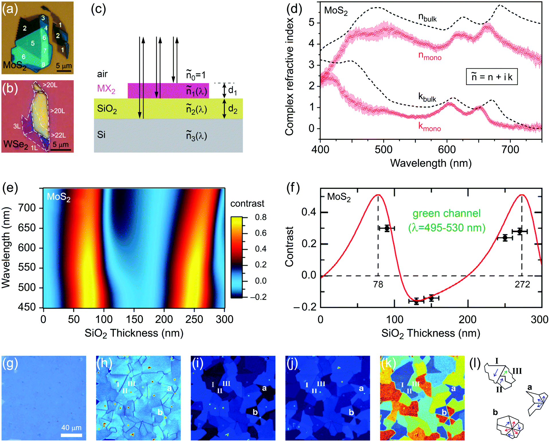 | ||
| Fig. 7 Optical microscopy characterization of MX2 nanosheets. (a and b) Optical microscope images of MoS2 and WSe2 flakes on SiO2(90 nm)/Si and SiO2(285 nm)/Si substrates, respectively. The number of layers at different locations is also given for MoS2. (c) Schematic of the stacking sequence and associated optical reflection and transmission paths. (d) Complex refractive indexes of bulk and monolayer MoS2. (e) Reference plot of the calculated contrasts for MoS2 on a SiO2/Si substrate as a function of illuminating light wavelength and SiO2 thickness. (f) Calculated and measured contrasts of MoS2 on a SiO2/Si substrate integrated over the green channel by using a green filter. (g) Ordinary linear optical image of a uniform MoS2 monolayer epitaxially grown by CVD on a SiO2(285 nm)/Si substrate. (h) Nonlinear second harmonic generation (SHG) image of the epitaxially grown monolayer MoS2 from the same region shown in the previous panel. (i and j) x-Polarized and y-polarized SHG images of the same area in the previous panel, respectively. (k) Colour-coded map of crystal orientations in the epitaxially grown monolayer MoS2, post-processed from the x-polarized and y-polarized data in two previous panels. (l) Schematic showing the crystal orientations of selected regions in the previous panel. Figure adapted with permission from: (a) ref. 258. Copyright 2013 American Chemical Society; (b) ref. 263. Copyright 2016 American Chemical Society; (d) ref. 255. Copyright 2015 Nature Publishing Group; (e and f) ref. 256. Copyright 2011 IOP Publishing Ltd; (g–l) ref. 259. Copyright 2014 American Association for the Advancement of Science. | ||
Fig. 7f suggests SiO2 thicknesses of approximately 78 and 272 nm are the most appropriate thicknesses for detection of MoS2 layers with the use of the green filter (which is more comfortable for eyes) as well as without any colour filter, in white light. These values are very close to the two widely accepted SiO2 thicknesses of 90 nm and 285 nm, experimentally optimized for observing G6-TMD nanosheets.258,259 Some investigators have used substrates with other oxide layers such as Al2O3/Si,260 or even totally different substrates such as quartz,168 but from the optical visibility point of view there is no evidence of improvement compared to the SiO2/Si substrate. For the SiO2/Si substrate both degenerately n-doped (n++)261 and p-doped (p++)262 Si (100) have been used depending on the desired application and this does not affect the visibility of MX2 layers. By achieving a good contrast the thickness of nanosheets can be calibrated experimentally or theoretically for identifying the number of layers. Post-measurements then can be carried out on selected nanosheets by AFM to precisely determine the thicknesses.
Aside from the identification and thickness estimation of G6-TMD nanosheets by normal light microscopy, a variation of it, called second harmonic imaging microscopy, has been recently employed259,264,265 as a powerful tool for determining the grain boundaries and crystal orientations within monolayer nanosheets, especially those grown uniformly over a large area by bottom-up methods, such as CVD. This technique relies on a two-photon process known as second harmonic generation (SHG) which is a nonlinear optical phenomenon. In SHG two photons of the same energy (produced by a laser) are absorbed by an electron to excite it to a virtual state. Then, upon relaxation the excited electron goes back into its ground state and emits a photon with exactly half the wavelength of the incident photons (frequency and energy doubled). Monolayers of MX2 have a broken inversion symmetry and consequently exhibit a strong SHG light due to their noncentrosymmetric structure.259Fig. 7g and h show comparative images taken by an ordinary light microscope and a second harmonic imaging microscope (pumped with a 1300 nm laser beam) from the same area of a monolayer MoS2, epitaxially grown by CVD on the SiO2(285 nm)/Si substrate. As can be seen from Fig. 7g, normal light microscopy only shows a uniform and continuous coverage of monolayer MoS2 on the substrate. However, probing the same window with a second harmonic imaging microscope reveals the polycrystalline nature of the layer due to the destructive interference and suppression of SHG light at grain boundaries (Fig. 7h).259 Moreover, refinement of this technique by analysing the x and y-polarized component of SHG light, generated by a linearly (x or y) polarized incident laser beam, can provide much valuable information regarding crystal orientation of single-crystalline domains within a polycrystalline monolayer film (Fig. 7j–l).
4.2. Photoluminescence spectroscopy
MX2 nanosheets exhibit a pronounced photoluminescence (PL) emission in comparison with their bulk counterparts. In particular, for MX2 monolayers the photoluminescence quantum yield exceeds 10000 times the bulk value, owing to the change in the band structure from indirect bandgap to direct bandgap going from bulk to monolayer, as discussed before in Section 3.8,266Fig. 8a shows two major direct electronic transitions (labeled A and B) at the K point of the Brillouin zone of MX2, that are primarily responsible for PL emission. Differentiation is made between MoX2 and WX2, due to different signs of spin splitting of the conduction band in molybdenum and tungsten dichalcogenides. The values of A and B transitions, as well as the exciton binding energies (Eb), valence band spin splitting (ΔVSO) and conduction band spin splitting (ΔCSO) for MX2 monolayers are listed in Table 2.
 | ||
| Fig. 8 Photoluminescence characterization of MX2 nanosheets. (a) Mechanism of photoluminescence emission in molybdenum dichalcogenide (MoX2) and tungsten dichalcogenide (WX2) nanosheets at the +K valley of the Brillouin zone. (b) PL spectra of MoS2 nanosheets of different thicknesses ranging from monolayer to fewlayer. The inset shows the relative PL intensity of WS2 nanosheets versus the number of layers as the typical trend of other MX2 along with the unusual behaviour of MoTe2. (c) UV-visible spectra of MX2 nanosheet dispersions in NMP. (d) Variation of electroluminescence spectra of WSe2 and MoSe2 with temperature from 6 to 300 K. (e) The effect of substrate on the PL spectra of MoS2 nanosheets. Schematics of a neutral exciton and a negative trion are also illustrated. (f) PL spectra of MoS2 monolayers with different solvent surroundings. Figure adapted with permission from: (b) ref. 267. Copyright 2014 The Royal Society of Chemistry, ref. 266. (WS2-inset) Copyright 2013 Nature Publishing Group and ref. 176. (MoTe2-inset) Copyright 2015 American Chemical Society; (c) ref. 271. Copyright 2015 Nature Publishing Group; (d) ref. 299. Copyright 2015 American Chemical Society; (e) ref. 286. Copyright 2014 The Royal Society of Chemistry; (f) ref. 288. Copyright 2013 Wiley. | ||
PL spectra of MoS2 ultrathin films with various numbers of layers ranging from monolayer and bilayer to fewlayer, as the typical spectra of other G6-TMD nanosheets, are shown in Fig. 8b. The emission spectra consist of two major peaks A and B which are more pronounced for monolayer and an additional broad peak I at higher wavelengths (lower energies) for bilayer and thicker nanosheets.8,267 This latter peak is attributed to the indirect transition from Kc to Γv for WSe2 and Λc to Γv for other MX2 (see Fig. 6c for the standard notation of band structure), as thoroughly investigated by Eda and coworkers.175 The broadening of peak I is due to its indirect nature and phonon-mediated transition. For the other two main peaks in PL spectra, A and B, full width at half maximum (FWHM) values represent the optical quality of the samples and lower FWHM values (sharp peaks) indicate higher crystal quality.268,269 Slight blue-shift of PL peaks to the higher energy by decreasing the number of layers is evidence for the increase in bandgap by thinning of MX2 nanosheets, as discussed in the previous section. It is worthwhile to note that although single layer 1H-MoS2 (semiconducting phase) shows a strong PL emission, 1T-MoS2 (metallic phase) does not have a PL signature.270
Another important aspect of PL spectra of MX2 nanosheets is presented in the inset of Fig. 8b, where the relative PL quantum yield is plotted versus the number of layers. While all monolayer MX2 nanosheets exhibit strong photoluminescence emission, their quantum yield (number of emitted PL photons to the number of incident photons) decreases rapidly by several orders of magnitude in bilayer and fewlayer nanosheets, as for example shown for WS2 in the inset.8,160,266 However, MoTe2 nanosheets have a unique and surprising thickness-dependent PL spectra. Lezama et al.176 who first reported this behaviour, which was then confirmed by others,139 attributed it to an unexpected crossover from indirect to direct bandgap in bilayer MoTe2 and nearly degenerate direct and indirect transitions in trilayer MoTe2.
The UV-vis absorbance spectra of G6-TMD nanosheet dispersions in NMP (N-methyl-2-pyrrolidone) solvent are shown in Fig. 8c.271 The two lowest energy features of A and B arise from the absorption of incident photons in direct excitonic transitions at the K point of the Brillouin zone, just as the reverse transitions occur in PL emission (see Fig. 8a).146,272–274 The positions of the A and B peaks for MX2 nanosheet dispersions are listed in Table 2. Also, two broad absorption peaks at higher energies, labeled C and D, are observed in UV-vis spectra which can be associated with direct excitonic transitions at the M point of the Brillouin zone (see Fig. 6c for the standard notation of band structure).275–277 UV-vis absorbance spectra of G6-TMDs have been systematically studied in the whole range of the spectrum by several investigators.146,147,278,279 More accurate inspection of the UV-vis spectra reveals two subsidiary peaks, known as A′ and B′, which are particularly pronounced and detectable in MoTe2132 and WSe2.272 These peaks are generally believed to be due to direct excitonic transitions from deep electronic states in the valence band to the conduction band at Γ or K points of the Brillouin zone;276,278,280 however, the exact underlying absorption mechanism remains to be elucidated and assigned.
UV-vis spectroscopy is a facile and ubiquitous method for measuring the concentration of liquid phase exfoliated nanosheets as well as the lateral size and thickness of nanosheets dispersed in various solvents. By measurement of the absorbance of a sample at the wavelength corresponding to the main characteristic absorption peak, i.e. peak A, for example 673 nm for MoS2 and 628 nm for WS2 according to Table 2, the concentration of nanosheets (C) can be related to the absorbance of the sample divided by the cell length (A/l) through the Beer–Lambert law, A/l = αC, where α is the absorption coefficient.281,282 The absorption coefficient of MoS2 at 679 nm has been reported to be ∼1020 ml mg−1 m−1.283 In the procedure of determination of concentration it is important to subtract the background from the UV-vis spectra before using the Beer–Lambert law to eliminate the effect of scattering.283–285 In fact, typical UV-vis spectrophotometers that are not equipped with integrating spheres measure the extinction spectrum rather than the absorption spectrum, while the former includes the share of scattering in the total spectra in addition to the absorption. Coleman and coworkers established two empirical equations relating the peak positions and intensities in extinction spectra of MoS2 dispersions to the average lateral size and number of layers of dispersed nanosheets.254
Overall, the PL characteristics of G6-TMDs are influenced by several factors, including substrates,286,287 solvents,288 strain,289 laser excitation intensity,290,291 defects,189,195,292 molecular physisorption,293 chemical doping,294,295 alloying296 and heterostructuring.297,298 Of particular interest is the temperature dependent PL spectra of MX2 which exhibit a striking difference between MoX2 and WX2 monolayers. Generally, the two direct excitonic peaks, A and B, in MX2 PL spectra imply the spin-splitting of the valence band with the difference providing a measure of this splitting (about ∼200 meV for MoX2 and ∼400 meV for WX2 monolayers, according to Table 2). On the other hand, the conduction band of MX2 nanosheets is also split by spin–orbit coupling and though it is an order of magnitude smaller than the valence band splitting, it has a great impact on the temperature dependent photoluminescence (PL) and electroluminescence (EL) spectra.299 While the PL and EL intensities of MoX2 monolayers decrease by increasing the temperature, the PL and EL intensities of WX2 monolayers increase by increasing the temperature. For example, as shown in Fig. 8d, the EL intensity of MoSe2 monolayers falls by about 10 times when the temperature is increased from 6 K to 300 K, whereas WSe2 monolayers exhibit about 200 times increase in the EL intensity in this temperature range.299 The increase in photoluminescence of WSe2 monolayers is also remarkable (about 10 times) going from 6 K to 300 K, very promising for light emitting quantum wells and other optoelectronic devices.299 The origin of this behaviour can be explained by considering the electronic band structure of MX2 in Fig. 8a. Since the conduction band splitting of MX2 compounds is small and comparable to kBT energy at room temperature (∼26 meV), the temperature has a strong influence on how excited electrons accumulate in the two adjacent spin–orbit induced states in the conduction band at the K point. At low temperatures, the exciton population in MX2 monolayers tends to accumulate in the lowest energy exciton sub-band which is bright in MoX2 monolayers and has strong EL and PL, while it is dark (decays through nonradiative recombination) in WX2 monolayers. In contrast, at room temperature there is enough energy for excited electrons and holes to accumulate in the second lowest energy exciton sub-band which is dark in MoS2 monolayers while it is bright in WX2 monolayers. The external quantum efficiency of light emitting quantum wells fabricated from monolayers of WSe2 sandwiched between h-BN (hexagonal boron nitride) fewlayer nanosheets and graphene electrodes was reported to be 5% at room temperature more than 250 times higher than devices fabricated by MoS2 or MoSe2 monolayers.299
There are two other noticeable trends in Fig. 8d, which deserve further discussion. First, by increasing the temperature, in both MoX2 and WX2 monolayers, the EL peaks shift to lower energies, a fact that is also observed for PL peaks.151,190,300 This shift can be understood in terms of change in the in-plane lattice constant, a, by temperature variation. Increasing the temperature causes an increase in a and similar to the in-plane tensile strain,301–303 this expansion leads to a decrease in the bandgap and thus the red-shift of EL and PL peaks. These shifts can be described by Varshni's semi-empirical equation, the relationship between the bandgap and temperature of common semiconductors.79,300 Another trend in Fig. 8d is peak broadening by increasing the temperature for both MoX2 and WX2 which is attributed to increased scattering of excitons by optical phonons at higher temperatures.300
Peak A, the main PL peak of MX2 nanosheets, is a superposition of a neutral exciton (A0) and a negative trion (A−). The binding energy of an exciton (an electron electrostatically bonded to a hole, see Fig. 8e) in MX2 monolayers is on the order of ∼600 meV, whereas a negative trion (two electrons electrostatically bonded to a hole, see Fig. 8e) has an excess binding energy of ∼20 meV with respect to an exciton and thus A− is redshifted compared to A0.142 The proportional share of excitons and trions in peak A of MX2 nanosheets strongly depends on the substrate or the solvent of nanosheets. For example, PL emission of freestanding MoS2 nanosheets, as well as supported MoS2 nanosheets on conducting and polymeric substrates, such as Au, graphene and gel-films, primarily originates from recombination of excitons (A0).287 In contrast, PL emission of MoS2 nanosheets on SiO2 and mica is dominant by emission from trions (A−) because of the n-type doping of MoS2 by these substrates and the presence of an excess electron which promotes effective formation of trions.287Fig. 8e shows the PL spectra of monolayer MoS2 on SiO2, gel-film and two common substrates for high performance electronic devices, LaAlO3 (LAO) and SrTiO3 (STO). Gel-film and SiO2 are commonly used as references for deconvolution of unknown peaks into exciton and trion components, respectively. It is evident from this figure that LAO induces electron doping into MoS2 and favours the formation of trions but not as much as the SiO2 substrate. Conversely, MoS2 on STO preserves its neutrality, like MoS2 on the polymeric gel-film, and exhibits an enhanced PL emission.286 The last panel in Fig. 8 shows the effect of different solvents with different dielectric constants and refractive indexes on the PL spectra of MoS2 monolayers.288 Compared with PL peaks in air, halogenated solvents cause blueshifts while nonhalogenated solvents cause redshifts.
The PL spectra of G6-TMDs are also influenced by the presence of defects in their crystal structures.228,229,304 Early works showed that while exposure to a high power (100 W) oxygen plasma totally quenched photoluminescence in monolayer MoS2,305 low power (5 W) oxygen plasma treatment could enhance photoluminescence thousands of times.190 PL quenching was explained by formation of disordered MoO3 regions within the MoS2 crystal,305 whereas PL enhancement was attributed to the formation of sulfur vacancies and subsequent adsorption of oxygen molecules on these defective sites.190 Oxygen adsorption induces p-doping and depletes excess electrons in naturally n-doped MoS2 and thus converts the dominant process of PL emission from trionic recombination to a much more effective process of excitonic recombination.190 Observation of a new defect-induced peak ∼0.1 eV below the main excitonic peak (peak A) of MoS2, MoSe2, WS2 and WSe2 at low temperatures has also been reported by several research groups.189,202,306 It is generally accepted that the origin of this peak is directly connected to chalcogen vacancies and it was proposed that the intensity ratio of this defect peak and the neutral exciton peak A0 (ID/IA0) can be used as a measure of the defect concentration in G6-TMDs.307 Detailed assessment of sulfur vacancy defects in monolayer MoS2 revealed that single sulfur vacancies (VS) can be characterized by a peak 0.1 eV below peak A, which rapidly vanishes by increasing the temperature because of the weak bonding between excitons and VS defects.189,308 However, double sulfur vacancies (VS2) produce a peak 0.2 eV below peak A, which can be clearly resolved at low temperatures and remains up to higher temperatures compared with the VS induced peak.202,308 Grain boundaries also have a strong effect on PL spectra and while mirror twin boundaries were reported to quench PL significantly, tilt grain boundaries led to considerable enhancement.183 Recently, cathodoluminescence (CL) spectroscopy of multilayer MoS2 flakes (fewlayer to 30-layer) has revealed two new peaks one in the near-infrared region around 0.75 eV due to sulfur vacancies and another at 0.98 eV presumably due to ripplocations (the interplay between surface ripples and crystallographic dislocations).309,310 This interesting finding provides a practical route to identify and quantify vacancies in fewlayer G6-TMDs where PL spectroscopy becomes ineffective due to indirect band-to-band transitions and weak emissions.
Aside from nanosheets, PL and UV-vis spectroscopy techniques are widely used to characterize G6-TMD quantum dots. Similar to the bandgap widening by going from bulk to monolayer which is due to the quantum confinement in one external dimension, downsizing to quantum dots causes further bandgap widening and a blue-shift to the higher energies for all peaks in both PL and UV-vis spectra due to the quantum confinement in all three dimensions. Other important features of optical characterization of G6-TMD quantum dots, such as excitation dependent PL peak positions and disappearance of UV-vis peaks with only a prominent peak in the UV region, can be found in the specialized literature.275,280,311,312
4.3. Raman spectroscopy
Raman spectroscopy as a fast and non-destructive technique is widely used to study the scattering of light by phonons and to characterize the structural and electronic properties of nanomaterials, on both laboratory and mass-production scales.313 The success of Raman spectroscopy in characterizing graphene314,315 led to the development of this technique for other layered materials including G6-TMDs.316As discussed in the crystal structure section, bulk 2H-MX2 has D46h space group and its primitive unit cell contains six atoms. Thus, the 2H-MX2 dispersion relation has 18 branches in which 3 are translational acoustic and the other 15 are optical branches. The irreducible representation of optical phonon modes at the zone centre Γ of the hexagonal Brillouin zone is:159,317
| Γ2H,optical = A1g(R) + A2u(IR) + 2B2g(S) + B1u(S) + E1g(R) + E1u(IR) + 2E2g(R) + E2u(S) | (1) |
 | ||
| Fig. 9 Raman characterization of MX2 nanosheets. (a) Typical room temperature Raman spectrum of the 2H-MoS2 single crystal with all Raman active modes labeled. (b and c) Atomic displacements of the Raman and infrared active modes of semiconducting trigonal prismatic (1H) and metallic octahedral (1T) polytypes of monolayer MX2. (d) Raman spectra of 1H- and 1T-MoS2 monolayer nanosheets in the backscattering geometry. (e) Evolution of Raman spectra from bulk 2H-MoS2 to monolayer 1H-MoS2. (f) Change in the E12g and A1g Raman modes (left vertical axis) and their difference (right vertical axis) as a function of the number of layers. Figure adapted with permission from: (a) ref. 335. Copyright 2008 BioMed Central Ltd; (d) ref. 329. Copyright 2014 Nature Publishing Group; (e and f) ref. 330. Copyright 2010 American Chemical Society. | ||
A monolayer MX2 crystal contains three atoms in its primitive unit cell and thus has 9 normal vibration modes, 3 of which are translational acoustic and the others are optical modes. The irreducible representations of six optical phonon modes at the Γ point for the monolayer 1H-MX2 (semiconducting phase) with D13h space group and 1T-MoS2 (metallic phase) with D33d space group are:159
 | (2) |
| Γ1T,optical = A1g(R) + A2u(IR) + Eg(R) + Eu(IR) | (3) |
The atomic displacements of these optical phonon modes are shown in Fig. 9b and c. Again “E” modes are in-plane and doubly degenerate with vibrations in longitudinal and transverse directions. The acoustic modes of 1H and 1T structures are represented by A2′′ + E′ and A2u + Eu, respectively.159 It is obvious that the absence of the Eu peak is the Raman fingerprint of 1T-MX2 as compared with 1H-MX2, which exhibits a strong peak in the corresponding frequency range due to the E′ mode.159
Fig. 9d shows the Raman spectra of 1H-MoS2 and 1T-MoS2. The broad peak at ∼450 cm−1 in the 1H-MoS2 spectrum, denoted as 2LA(M), is attributed to the second-order overtone of longitudinal acoustic phonons at the M-point of the Brillouin zone (see Fig. 6b for the standard notation of the Brillouin zone of a hexagonal lattice).320,326,327 Moreover, as stated before, the E′′ mode is forbidden under the backscattering configuration.318–320 In the 1T-MoS2 spectrum, along with the absence of the Raman inactive mode Eu, there are additional peaks at 154, 204, 310 and 356 cm−1 which can be explained by the formation of a superlattice during synthesis and are attributed to the Brillouin zone-edge phonons.116,328,329
The frequencies, widths and intensities of the Raman E12g and A1g peaks are affected by the thickness of MoS2 nanosheets.150 Interestingly, the change in the frequencies by the change in the thickness is monotonic and thus it can be used as a “thickness indicator”.330Fig. 9e shows the evolution of the E12g and A1g modes of the Raman spectra of MoS2 nanosheets by changing the number of layers. Variation of the frequencies of the E12g and A1g modes and their difference (Δω) with change in the number of layers is also shown in Fig. 9f. The out-of-plane A1g mode is influenced more by decreasing the layer number than the in-plane E12g mode. The frequency difference of these two characteristic modes ranges from 19 cm−1 in the 1H-MoS2 monolayer to 25 cm−1 in bulk 2H-MoS2.150 The increase in the A1g mode frequency by increasing the number of layers is attributed to the interlayer van der Waals force enhancement and stiffening of the MoS2 crystal as a whole.112,150 On the other hand, going from monolayer to bulk the E12g mode frequency decreases, because of increased dielectric screening of the Coulombic interlayer interaction and stacking-induced change of the interlayer bonding.112,323 Other MX2 nanosheets also exhibit a similar trend and their corresponding peak shifts are listed in Table 2.
As the PL spectra, Raman spectra of G6-TMDs are also affected by the presence of defects.228,229 Analysis of the intentionally defected MoS2 monolayers by ion bombardment,331,332 plasma etching333 and electron irradiation334 revealed that with increasing defect density the peak positions of the main first-order  and E′ peaks blueshift and redshift, respectively. In addition, this increase in the separation of the peaks is accompanied by peak broadening.331,334 Considering the simple relation of a harmonic oscillator (
 ), the redshift in the peak position of the in-plane E′ mode can be explained by the weakening of the restoring force constant due to sulfur vacancies and the absence of some Mo–S bonds.334 On the other hand, a decrease in the total mass of the vibrating system and allowing vertical oscillations of originally static Mo atoms can rationalize the blueshift and increase in the peak position of the out-of-plane
  mode.334 Activation of several new second-order peaks, originating from the edges of the Brillouin zone, was also reported.331 Most importantly, longitudinal acoustic phonons at the M-point of the Brillouin zone cause a prominent peak, called LA(M), which is around 227 cm−1 for monolayer MoS2. It was proposed that the intensity ratio of this defect-activated peak to either of the main first-order peaks (
 or E′) can be used as a quantification tool for the number of defects in G6-TMDs, in analogy with the intensity ratio of D and G peaks (ID/IG) in graphene.331 Recently, observation of a new peak at 450 cm−1 almost exclusively due to sulfur vacancies, and several satellite peaks resulting from Mo and MoS6 vacancies, has also been reported.332
Li et al.150 have systematically measured the Raman frequencies of E12g and A1g modes with various laser lines from ultraviolet to visible for MoS2 flakes with thicknesses ranging from monolayer to bulk and provided a reference table. The effect of laser power on the Raman peak frequencies of E12g and A1g modes was investigated by Yan et al.165 and it is found that above 0.3 mW, nonlinearity in the peak positions occur. In the linear region, both modes soften and red shift toward lower values upon increasing the laser power. The effect of the substrate on the Raman peaks was studied by Buscema et al.287 who utilized various dielectric and conducting substrates such as SiO2, mica, Au, and h-BN. They reported that while the E12g mode is not sensitive to the substrate, the peak position of A1g mode shows a sizeable shift of up to 2 cm−1 by changing the substrate. Temperature326 and pressure336 dependences of Raman spectra of MX2 monolayers have been also systematically investigated. As a general rule, increasing the temperature causes a downward shift in Raman peaks, whereas increasing the pressure causes upward shifts. Raman selection rules for fewlayer MX2 nanosheets with an odd or an even number of layers, effect of external perturbations such as strain and electric field on Raman active modes as well as resonant Raman spectrum of MX2 were comprehensively reviewed by Tan and coworkers.313 Recently, several high quality and in-depth review articles have been published on Raman characterization of G6-TMD nanomaterials to which interested readers are referred for further details.320,337,338
5. Production methods
This section provides a systematic classification of all existing production methods of various group 6 transition metal dichalcogenide nanomaterials with a detailed description and discussion of each method from an application-oriented point of view. Production methods are first categorized into top-down and bottom-up approaches. Then, top-down methods are divided into four main subcategories of 5.1. Mechanical cleavage, 5.2. Liquid phase exfoliation, 5.3. Intercalation and exfoliation, and 5.4. Thinning. Bottom-up methods are also divided into two main subcategories including 5.5. Vapour deposition and 5.6. Solution-based synthesis. Finally, these six main subcategories are further segmented into 13 distinct types of production methods as presented in Fig. 10. | ||
| Fig. 10 A complete classification of all existing production methods of G6-TMD nanomaterials. | ||
Discussion of each production method starts with a clear, readily understandable and step-by-step explanation of its procedure for a wide interdisciplinary audience. The pertinent chemical reactions, the physical mechanisms involved in the process and the governing equations as well as starting materials, necessary equipment and safety concerns are then discussed in detail. With the aid of original schematics and charts together with carefully collected and arranged figures and tables, the effects of various general processing parameters such as temperature, pressure and time, along with individual parameters of each production method on the quality and quantity of produced nanosheets are described. While our emphasis is on 2D nanosheets, we also review and discuss the capability of producing other nanomaterials such as 0D quantum dots, 1D nanoribbons and 3D nanoflowers, for each specific production method. The major criteria in utilizing the production method for technological applications, including thickness, lateral size, production rate and crystalline quality of produced nanosheets, are subsequently analysed and summarized. In addition, challenges and practical issues related to each production method are addressed and remarks on its advantages and disadvantages are provided. Finally, the devoted subsection to each production method is culminated by outlining potential future research directions to improve that method.
It should be emphasized that the presented classification here reflects our application-oriented perspective and is just one of several possible classifications for existing production methods of G6-TMD nanomaterials. Some of these production methods can be further divided into two or three methods and each of them has the potential to be considered as an independent production method. For instance, metal–organic chemical vapour deposition (MOCVD), epitaxial growth and atomic layer deposition (ALD) are all considered here as subcategories of the chemical vapour deposition (CVD) method; however, they could be treated separately in dedicated sections. On the other hand, some authors have preferred to include thermal decomposition as a subcategory of CVD,32,41 while we consider it as an outstanding production method and place it under the solution-based synthesis branch. We also consider laser thinning and thermal annealing as sub-categories of the sublimation production method, and sputter deposition, pulsed laser deposition (PLD) and thermal evaporation deposition as subcategories of the physical vapour deposition (PVD) method. Nevertheless, we believe that our particular classification provides a cognitive framework to discuss all existing production methods of G6-TMDs in a balanced way with a unified approach avoiding confusion that might arise from a long and indiscriminate list of methods. Furthermore, this classification can effectively help outline the future research directions that should be explored to improve existing production methods or develop new methods, either from scratch or by combining different production methods into one method that benefits from their advantages and eliminates the weak points of each individual method.
5.1. Mechanical cleavage
In Fig. 11 the main steps of the method are illustrated. Starting from a single crystal with a flat surface of about 1 × 1 cm2, the standard thinning procedure involves successively peeling layers of the crystal using an ordinary adhesive tape (for example 3M Scotch® tape). First, some initial cleavage steps are performed to achieve a fresh surface of the MX2 crystal and then this fresh basal plane is placed on the sticky side of a piece of tape. By peeling off the tape a layer of about 1 μm in thickness is separated from the crystal. Then another piece of tape is placed on the other side of the separated layer to form a sandwich made of tape/MX2/tape. By pulling the two pieces of tape apart the layer splits into two thinner layers of the same surface area. This process is usually performed by repeated folding and unfolding of the tape, until the layers adhered to the tape at its surface become barely visible to the naked eye. The next step consists of sticking the tape to a silicon substrate covered with usually 90 or 285 nm thick SiO2 and applying a light rubbing with a soft object such as a dry sponge.258,259,340 Finally, peeling off the adhesive tape leaves behind flakes of MX2 on the substrate.
 | ||
| Fig. 11 Micromechanical cleavage method. (a) Peeling a micrometre-thick layer off a bulk MX2 crystal by a piece of adhesive tape. (b) Successive thinning of the separated layer until the layer adhered to the tape becomes barely visible to the naked eye. (c) Sticking the tape with the adhered nanometre-thick MX2 layer onto a SiO2/Si substrate and rubbing lightly with a dry sponge. (d) Peeling off the adhesive tape and using an optical microscopy to locate and identify randomly sized MX2 nanosheets. | ||
Typical size of MX2 layers obtained from the micromechanical cleavage technique is in the range of 25 to 200 μm2.8 However, searching for rare and hidden monolayers in a haystack of thousands of thicker flakes distributed on the substrate over an area of about 1 cm2 is only possible with an optical microscope which has a comparatively large field of view (∼0.05 mm2 at 1000×) together with a sufficient resolution and contrast. After locating and identifying monolayer and fewlayer nanosheets, more accurate analyses can be performed by atomic force microscopy (AFM) and Raman spectroscopy.
Fig. 12a–h shows exemplary optical microscopy and corresponding AFM images of single to quadrilayer of MoS2 on SiO2/Si substrates (300 nm SiO2). Under white light illumination with a 100× objective lens, the bare Si substrate with a 300 nm SiO2 capping appears bluish-purple while the regions covered with MoS2 flakes are in different colours and contrasts from faint purple for monolayer and light blue for few-layer to completely white for thick flakes.258,341Fig. 12i and j also shows a typical optical image and the corresponding colour chart for determining the number of layers of deposited and suspended MoS2 nanosheets, along with verification of the assigned number of layers by AFM.
 | ||
| Fig. 12 Micromechanically exfoliated monolayer and fewlayer MoS2 nanosheets on SiO2/Si and their identification based on colour contrast. (a–d) Optical microscope images of monolayer, bilayer, trilayer, and quadrilayer MoS2 nanosheets. (e–h) Corresponding AFM images of panels (a–d), respectively. (i) Optical image of an 8-layer MoS2 flake placed on top of a 285 nm pre-patterned SiO2/Si substrate and corresponding colour chart for determining the number of layers based on regions lying on the substrate (supported) or regions covering holes (suspended). (j) AFM image of the highlighted square in the previous panel with a height profile along the dashed line. Figure adapted with permission from: (a–h) ref. 342. Copyright 2012 Wiley-VCH; (i and j) ref. 343. Copyright 2012 Springer. | ||
The SiO2/Si substrate should thoroughly be cleaned before sticking the tape on to it. A conventional procedure consists of a standard RCA cleaning followed by boiling in acetone and isopropyl alcohol for 5 min and finally, cleaning by oxygen plasma again for 5 min.341 After peeling the tape off the substrate some residue might be left, but most of the time it can be removed simply by cleaning the substrate with isopropanol.344 For a more rigorous cleaning, the wafer could be immersed in acetone for 6 h, followed by the acetone, methanol, and isopropanol washing for 30, 15, and 30 s, respectively.345 This latter cleaning has the added advantage of removing many of the thick undesired flakes, while thin flakes (less than 10 layers) remain attached to the substrate due to van der Waals and capillary forces.
Besides the above discussed established route for micromechanical cleavage, there have been several attempts to improve this method towards higher throughput, especially a higher yield of monolayers, and simultaneously achieving larger flake sizes. Huang et al.346 by careful cleaning of the SiO2/Si substrate and annealing the substrate after sticking the tape to it for 2–5 minutes at 100 °C on a conventional hotplate, before peeling off the tape, achieved yield and flake sizes several times higher than the routine micromechanical cleavage method. Another interesting idea to improve the mechanical cleavage method is to use of a gold film as an intermediate substrate to cleave bulk G6-TMD crystals right at the topmost layer. Gold has a strong affinity towards chalcogens and thus can overcome the van der Waals interaction between the topmost layer and the rest of the crystal more effectively than SiO2. Magda et al.347 and Desai et al.348 employed this concept to modify the routine micromechanical cleavage method by including an additional gold-mediated transfer step and obtained large areas of various monolayer G6-TMDs with high yield and lateral sizes up to 500 μm.
 | ||
| Fig. 13 Nanomechanical cleavage method. (a) Schematic of the nanomechanical cleavage method. (b) A TEM image of the tungsten probe and a bulk MoS2 flake loaded on the edge of a gold wire. (c and d) An HRTEM image of the tungsten tip and atomic layers of a MoS2 flake at initial contact and after nanomechanical cleavage of an 11-layer nanosheet. (e and f) An HRTEM image of a biased oxidized tungsten tip and a 9-layer MoS2 nanosheet at initial contact and after exfoliation of the top most monolayer by shearing. (g) Schematic of the nanomachining by an AFM tip. (h) An AFM image of an MoS2 flake patterned with single-layer precision. Figure adapted with permission from: (a–d) ref. 349. Copyright 2014 Nature Publishing Group; (e and f) ref. 351. Copyright 2015 American Chemical Society; (g and h) ref. 352. Copyright 2015 Springer. | ||
Tang et al.349 demonstrated a successful selective nanomechanical cleavage of MoS2 nanosheets from monolayer up to 23-layer nanosheets. They found three thickness dependent kinetic regimes for bending of fewlayer MoS2 flakes, during the cleavage process. Nanosheets with less than 5 layers bend homogenously with the same curving and rippling of all layers. Nanosheets of ∼10 layers bend with interlayer sliding and thick nanosheets of ∼20 or more layers bend with the formation of kinks. By using the tip of a scanning tunnelling microscope for nanomechanical cleavage, Casillas et al.350 reported that in the flexible regime of bending (<5 layers), the flexibility of a 3-layer nanosheet is the same as a monolayer nanosheet, while its elastic modulus is ∼200 times higher, promising for flexible electronics. Oviedo et al.351 also employed nanomechanical cleavage to study the interlayer sliding in MoS2 (Fig. 13e and f). They used an oxidized tungsten tip at a +10 V dc bias and found the shear strength of MoS2 to be 25.3 ± 0.6 MPa in the [120] direction under zero normal load. Furthermore, Miyake and Wang352 used the diamond-like carbon coated Si tip of an atomic force microscope (AFM) with a radius of less than 50 nm, to process a single-layer level manipulation of the MoS2 surface (Fig. 13g). As an example of nanomechanical cleavage by AFM, a fabricated heterostructure of latticed grooves with 200 nm line intervals and a processing depth of 0.6 nm is shown in Fig. 13h.
Even though the nanomechanical cleavage method is still at its early stages of development and needs sophisticated facilities, it is very well suited for applications in which a high quality nanosheet with a predetermined number of layers is required. Moreover, this method is of particular interest for atomic-scale machining as well as fundamental studies on elasticity and bending kinetics of nanosheets, interlayer sliding and kinking characterization and surface energy determination. Recently, there have been excellent reviews on in situ manipulation and characterization of nanomaterials at the atomic scale, in which interested readers can find more details.353,354
5.2. Liquid phase exfoliation
Liquid phase exfoliation (LPE) is one of the most widely used methods to produce MX2 nanomaterials (nanosheets and quantum dots) which is a simple and easy to implement yet powerful method. LPE consists of three major steps: (1) dispersion of the bulk MX2 powder in an appropriate solvent, (2) exfoliation of the bulk layered material into nanosheets with the development of shear stress in solution by a sonicator or a shear mixer (if required, stabilizing the dispersion with the aid of surfactants), and finally (3) separation of nanosheets and size-selection via centrifugation. Liquid phase exfoliation is a versatile method and when its setup is prepared, a range of other layered materials from graphene355–358 to phosphorene359–362 and boron nitride281,363,364 can be exfoliated with proper adjustment in parameters. The produced nanosheets are of high quality, free from defects on the basal plane and unoxidized.365 Furthermore, LPE is scalable and one of the leading candidates for commercial production of layered materials. The outcome of this method, i.e. a stable dispersion of nanosheets in a liquid medium, can be applied to a variety of environments or deposited on different substrates which is desirable for many applications such as thin film transistors, inkjet printed electronics, conductive electrodes for photovoltaics, energy storage and nanocomposites.40 Based on the energy source used to exfoliate and disperse nanosheets, research on liquid phase exfoliation is divided into two main routes: (1) sonication and exfoliation, (2) shear exfoliation. In the following subsections, these two routes are discussed in detail. | ||
| Fig. 14 Sonication and exfoliation method. (a) Schematic of the general procedure. (b) Photograph shows typical dispersions of G6-TMD nanosheets, exfoliated in water with the aid of a surfactant (sodium cholate, SC). (c) Absorbance per unit cell length (proportional to the concentration) of MoS2 nanosheet solutions for the best 20 solvents of MoS2. (d) Effect of surfactant type on the concentration of MoS2 nanosheets in aqueous media. (e) Concentration of MoS2 dispersions as a function of sonication power, surfactant concentration, initial concentration of bulk MoS2 powder and sonication time, all after 1500 rpm centrifugation. (f) Schematic of a cascade centrifugation procedure to achieve a dispersion of WS2 in water/SC with a highly enriched monolayer nanosheet. Figure adapted with permission from: (b) ref. 279. Copyright 2016 The Royal Society of Chemistry; (c and d) ref. 281. Copyright 2011 American Association for the Advancement of Science; (e) ref. 366. Copyright 2011 Wiley-VCH; (f) ref. 383. Copyright 2016 American Chemical Society. | ||
There are a number of research groups around the world, including the Coleman group at Trinity College Dublin and the Ajayan group at Rice university, that systematically used liquid phase exfoliation and produced nearly all sort of 2D layered materials in numerous liquid media.40,281,282Fig. 14b shows an example of various G6-TMD nanosheets exfoliated in aqueous media by sonication in water/surfactant solution. Very recently, Backes, Coleman and coworkers have shared their established procedure for exfoliating, characterizing and processing 2D layered materials in a guideline article367 and also provided a tutorial video publication.371 The sonication and exfoliation method has an active community with rich literature and the subject has been extensively reviewed in recent years.40,42,356–358,370,372 In the following discussion we only highlight the main ideas and research frontiers that we think need to be emphasized or clarified to gain an insight into the entire field and stimulate further studies.
Coleman et al.281 surveyed a wide range of solvents (more than 1000 solvents) in the solubility parameter framework through a series of systematic experiments and suggested the best 20 solvents for MoS2 (Fig. 14c) and WS2. The A/l values for solvents given in Fig. 14c are the absorbance of samples at a wavelength of 672 nm (characteristic excitonic absorption peak of fewlayer MoS2 according to Table 2) divided by the cell length in the UV-vis absorption spectrum. As stated in Section 4.2, the A/l value is linearly proportional to concentration by the relation A/l = εC, known as the Beer–Lambert law, where ε is the extinction coefficient.281 O’Neill et al.283 reported MoS2 concentrations as high as 40 mg ml−1 in NMP by using long time probe sonication (200 h) and optimizing sonication conditions, in particular the initial MoS2 powder concentration (100 mg ml−1).
However, most good solvents of G6-TMDs, such as CHP, NMP and DMF, have high boiling points which become problematic when the fast removal of solvent is required for example in thin film deposition, inkjet printing or fabrication of polymer composites. Besides, solvents such as NMP and DMF are toxic and cause environmental issues. In addition, some applications such as biomedical diagnosis need biocompatible dispersions which urge the use of aqueous solutions. But, since G6-TMD nanosheets are hydrophobic in nature373 even after exfoliation in water (for example with long time sonication) they tend to aggregate, unless a surfactant is used. Thus another strategy in the sonication and exfoliation method is to first select a solvent depending on the application and then use surfactants to promote exfoliation and stabilization of nanosheets in the selected solvent. For sonication and exfoliation of MX2 in water or low boiling point solvents, a variety of ionic surfactants366,374 and nonionic surfactants366,368 as well as polymers66,375,376 have been used in the literature. The stabilization mechanism of dispersion is electrostatic repulsion for ionic surfactants and steric repulsion (space constraints) for nonionic surfactants or polymers.357,374 Smith et al.366 studied the dispersibility of various inorganic layered compounds, including MoS2, MoSe2, MoTe2 and WS2, in a number of ionic and nonionic aqueous surfactant solutions and found that under the same synthesis conditions the final concentration of stabilized nanosheets varies from 0.06 to 0.09 mg ml−1 for the range of surfactants used (Fig. 14d). Sonication and exfoliation assisted by non-conventional surfactants, such as DNA/RNA nucleotides,377 bovine serum albumin protein378 and gelatin,379 have also been reported. Gupta et al.374 measured the zeta potential of MoS2 surfactant stabilized dispersions with two representative cationic (cetyltrimethylammonium bromide, CTAB) and anionic (sodium dodecyl sulfate, SDS) surfactants and concluded that surfactant chains lie randomly on basal planes of MoS2 nanosheets while surfactant charged headgroups control the effective charge of nanosheets. Thus, cationic surfactants give positively charged nanosheets in the dispersion and anionic surfactants result in negatively charged nanosheets. It is worth noting that usually G6-TMD nanosheets dispersed in organic solvents or aqueous media without surfactants are negatively charged due to rather large electron affinity of sulfur atoms.273,380
Final concentration of dispersed and stabilized nanosheets in a solvent is an important parameter in the sonication and exfoliation method. Final concentration is typically in the range of 0.01 to 10 mg ml−1 and depends on the type of solvent (or surfactant for aqueous media), power of sonication, sonication time, initial concentration of the bulk powder, initial concentration of the surfactant (for aqueous media), centrifugation rate and centrifugation time.283,366 As shown in Fig. 14e, final concentration is monotonically increased by increasing the sonication power. Final concentration also scales with the square root of sonication time and increases by increasing the sonication time. Increasing the initial concentration of the bulk powder or the surfactant also increases the final concentration; however, there is an upper limit for these initial concentrations above which the final concentration does not increase or even decreases. Moreover, the final concentration exhibits an inverse correlation with centrifugation rate and time as a result of nanosheet sedimentation during centrifugation. Though the above discussion and trends generally hold for both organic solvents and aqueous media subjected to probe or bath sonication, there are other subsidiary effects and phenomena that may influence the specific behavior of each case. For example, Qiao et al.381 investigated the effect of sonication power on the concentration of MoS2 dispersions in NMP using a probe sonicator and found that the optimal range is from 200 W to 320 W for 20 ml solvent. Above 320 W the concentration decreased due to the cavitation shielding effect and increased population of bubbles around the sonicator tip. Han et al.382 then showed that the optimal power can be lowered to ∼6 W for 200 ml solvent by adjusting the depth of the sonicator tip to the dispersion surface.
In addition to the concentration, the size of the produced nanosheets is a key parameter. The mean lateral dimension and thickness can be directly measured and statistically analyzed by microscopic techniques, such as AFM and TEM, on drop-cast samples. The dynamic light scattering technique is also widely used for the in situ measurement of lateral size.253 Recently, a powerful technique based on optical extinction spectra has been developed to in situ measure concentration, mean lateral size and thickness of exfoliated nanosheets in a dispersion, simultaneously.254,367 Measurements show that the sonication process favors asymmetric nanosheets with mean length, 〈L〉, approximately twice the mean width, 〈W〉, and both usually below 1 μm.254 Furthermore, although some monolayers are always found in the dispersion the majority of exfoliated nanosheets are fewlayer consisting of 2–5 layers.254 Generally, lateral dimensions of nanosheets in the final dispersion are decreased by inverse square root of sonication time  and centrifugation rate
  , while the number of layers or the thickness of nanosheets, 〈N〉, is nearly independent of sonication time and decreases linearly with increasing centrifugation rate (〈N〉 ∝ 1/ω).283,366
A dispersion of nanosheets immediately after sonication has a broad distribution of lateral sizes and thicknesses and sorting of nanosheets in a more uniform dispersion with narrow size ranges is of great demand and interest for subsequent applications. Centrifugation-based sorting techniques are the most viable and effective approaches to this end which in general can be divided into three major strategies, namely: (i) sedimentation-based separation, (ii) density gradient ultracentrifugation and (iii) rate zonal separation.369,370
Sedimentation-based separation is the most versatile strategy to sort nanosheets which relies on the weight differences between nanosheets of different sizes in the dispersion. With this technique thick and large nanosheets which are heavier can be separated from thin and small nanosheets which are lighter. Upon centrifugation at moderate speeds (1000–6000 rpm) thick and large nanosheets precipitate at the bottom of the centrifugation tube while thin and small nanosheets can be extracted from the supernatant.384 Based on this concept, a size selection procedure by using cascade centrifugation has been developed to achieve dispersions of highly enriched monolayer nanosheets as exemplified in Fig. 14f for an aqueous WS2 dispersion with 75% monolayer content.383,385 In fact, step by step increasing of the centrifugation rate decreases the probability of trapping light-weight and small monolayer nanosheets between heavy and large flakes during sedimentation. A reverse procedure, by starting from a high centrifugation rate (∼5000 rpm) and then adding a fresh solvent to the sediment and extra centrifugation at lower speeds, step by step down to 300 rpm, has also been proposed to collect flakes with large lateral sizes of the order of 2 μm.283 In sedimentation-based separation the thickness and lateral size of the separated nanosheets are strongly correlated and large monolayers are not accessible. Density gradient ultracentrifugation, which relies on the density difference rather than the weight difference, can be used to separate nanosheets based on their thicknesses.386,387 In this technique, the surface of nanosheets is wrapped with amphiphilic block copolymer surfactants with the consequence that the density of thin nanosheets due to their larger surface to volume ratio decreases more than thicker nanosheets which allow separating them from each other.386 The rate zonal separation strategy is also available to sort nanosheets based on their lateral sizes along the centrifugation tube relatively independent of their thicknesses.19,38 This technique is based on the differences in the sedimentation coefficient of nanosheets of different lateral sizes which itself is inversely proportional to the frictional drag coefficient of nanosheets, a strongly size dependent property.254,369
One of the strong points of liquid phase exfoliation is the feasibility of solvent exchange. In this context, 2D crystals can be exfoliated in an appropriate solvent and then the solvent can be exchanged to a more favorable solvent for the target application, without degradation in quality or concentration of dispersed nanosheets. There are two general strategies for solvent exchange. In one strategy, a high centrifugation rate is employed to precipitate all nanosheets from the initial solvent and then the wet sediment is re-dispersed in the desired solvent by mild sonication.388 The key point is to avoid complete drying of the sediment which results in restacking of nanosheets. Thus, the sediment should transfer to the new solvent while it is still wet. To eliminate the trace of initial solvent, several cycles of centrifugation and re-dispersion may be required. Tang et al.388 prepared dispersions of MoS2 nanosheets in a wide range of organic solvents, including tetrahydrofuran (THF), acetone, methanol, ethanol and 1-butyl-3-methylimidazolium chloride ionic liquid through solvent exchange of originally exfoliated MoS2 nanosheets in water. In another strategy, the second solvent with a substantially higher boiling point is added to the initial solvent and the first one is evaporated simply by heating the dispersion.389 Ostling and coworkers389 exfoliated MoS2 nanosheets in DMF by bath sonication and then exchanged the low-viscosity and toxic DMF with high-viscosity and non-toxic terpineol for inkjet printing applications.
Combined sonication with grinding,275,390,391 ball milling,392 chemical exfoliation,388 quenching in liquid nitrogen,393 as well as sonication in pressurized bath,394 sonochemical breaking of nanotubes395 and H2O2-prompted sonication194,396 have also been reported for a higher degree of exfoliation or more control over the exfoliation process. Of particular interest, Yao et al.397 reported a high concentration of 27 mg ml−1 in an aqueous solution by pre-grinding MoS2 powder with a pestle and mortar and then sonication in a 45% ethanol/water mixture. Sonication in superacids is also an effective way to exfoliate bulk G6-TMDs.148,398 Pagona et al.148 bath sonicated bulk MoS2 and WS2 in chlorosulfonic acid and obtained nanosheets that, while preserving their semiconducting nature, were soluble in water, NMP and DMF at high concentrations. The mechanism of exfoliation by superacids is the reversible protonation (not oxidation) of constituent layers of bulk crystals and their stabilization in the dispersion through electrostatic repulsion due to delocalized partial positive charge at the edges of layers.399,400 Another important recent trend to solubilize G6-TMDs in common solvents, especially in water, is functionalization of nanosheets either at the edge or basal plane, which can be achieved for example by sonication in the presence of metal acetate salts,401 polyacrylic acid402 or amphiphilic copolymers.403
Aside from nanosheets, G6-TMD quantum dots (QDs) can also be produced with the sonication and exfoliation method. Gopalakrishnan et al.280 bath-sonicated bulk MoS2 powder in NMP for 3.5 h followed by 3.5 h probe sonication and then centrifugation at 5500 rpm to obtain interspersed MoS2 quantum dots in MoS2 fewlayer nanosheets. Ali et al.404 added an extra pre-grinding step in NMP to the aforementioned procedure and obtained blue luminescent MoS2 quantum dots with an average size of 2–5 nm. Zhang and coworkers46 also synthesized various G6-TMD quantum dots, including MoS2, MoSe2, WS2 and WSe2 by sequential grinding, sonication, centrifugation and filtration. They produced quantum dots in NMP and then easily separated quantum dots from NMP by adding n-hexane (poor solvent of MX2 QDs) and then chloroform (less polar solvent than NMP) to the dispersion and finally precipitated MX2 QDs by centrifugation. The produced quantum dots by this method can be easily re-dispersed in other polar and low boiling point solvents, such as water and ethanol. Recently, Zhao et al.405 have also reported production of WS2 quantum dots by probe sonication in aqueous solution with nonionic surfactants.
 | ||
| Fig. 15 Shear exfoliation method. (a) Photograph shows a typical high shear laboratory mixer. (b) Configuration of the rotor and stator in the mixing head of the laboratory mixer. (c) Schematic of the mixing mechanism in the laboratory mixer. (d) Photograph shows a typical kitchen blender. (e) The 4-blade impeller of the kitchen blender. Figure reproduced with permission from: (a–c) ref. 365. Copyright 2014 Nature Publishing Group; (d and e) ref. 273. Copyright 2015 American Chemical Society. | ||
The mechanism of shear exfoliation can be explained by considering the local shear rate generated by the mixer in the dispersion which causes adjacent liquid layers locally slide against each other. The local shear rate is proportional to the tangential force per unit area at each point in the liquid. When the local shear rate exceeds a critical value of ![[small gamma, Greek, dot above]](https://www.rsc.org/images/entities/i_char_e0a2.gif) min > 104 s−1 for bulk MX2 layered materials, the liquid–solid interaction overcomes the inter-layer solid–solid interaction which causes the outer atomic layers of the dispersed powder peel off from the bulk material.365
min > 104 s−1 for bulk MX2 layered materials, the liquid–solid interaction overcomes the inter-layer solid–solid interaction which causes the outer atomic layers of the dispersed powder peel off from the bulk material.365
In a high shear laboratory mixer, processing parameters are the mixing time (t), mixing volume (V), rotor speed (N), rotor diameter (D) and initial bulk powder concentration (Ci). The final concentration of exfoliated nanosheets (C) can be related to these processing parameters through an empirical master equation for any solvent which for example in the case of MoS2/NMP was reported as below:365
| CMoS2 ∝ t0.56Ci0.7D1.8V−0.5N1.3 | (4) |
According to eqn (4), the final concentration increases sublinearly with increase in mixing time while the initial concentration increases superlinearly with increase in the rotor speed and the rotor diameter. Although increasing the mixing volume decreases the final concentration, the total production of flakes (V × C) increases with the square root of mixing volume.
In the high shear mixer the maximum shear rate occurs in the gap between the rotor and stator, thus the majority of exfoliation takes place in this space.365,406 The shear rate can be estimated from ≈ πND/ΔR, where ΔR is the rotor–stator gap.365 Thus the combination of N, D and ΔR must be such that the condition of > 104 is fulfilled. It is shown that the turbulence regime, Re = ND2ρ/η > 104, is not necessary for exfoliation (ρ and η are liquid density and viscosity, respectively) and with Reynolds number below 104, exfoliation can be achieved, too.365 Shear exfoliation of various G6-TMDs, including MoS2, MoSe2, MoTe2 and WS2 in NMP365 and water/ethanol mixture,407 has been reported.
A kitchen blender has also been used to exfoliate layered materials, such as graphene, MoS2 and WS2, recently.273,406,408 As for a shear mixer, there is an empirical master equation which relates the final concentration to processing parameters. For surfactant assisted (sodium cholate) exfoliation of MoS2 in aqueous media, the below equation was reported:273
 | (5) |
Concentrations as high as 0.4 mg ml−1 and production rates up to 1.3 mg min−1 have been reported for the MoS2 liquid phase exfoliation with a kitchen blender.273 The main processing parameter of this method is surfactant concentration which greatly influences the final nanosheet concentration as well as their lateral size and number of layers. Nanosheets with controllable lateral sizes in the range of 40–220 nm and layer numbers of 2–12 layers were obtained by adjustment of Csurf.273 Other processing parameters have lower impact on the size and thickness of nanosheets in comparison with Csurf. In the kitchen blender method, the final exfoliated flake size and thickness are proportional to each other and by tuning the processing parameters, either large thick flakes or small thin flakes can be obtained and the aspect ratio (length/thickness) is rather constant.273
It is evident by comparing eqn (4) and (5) that the mixing volume (V) has a larger exponent in kitchen blenders than in high shear mixers, which implies that the exfoliation is done more effectively in a kitchen blender jar. In fact for a typical kitchen blender with 2000 W motor and rotation speed on the order of 8000 rpm, the fluid regime is fully turbulent273,408 and local exfoliation take places everywhere in the blender jar which is more effective than the exfoliation at the small gap between the rotor and stator in a high shear mixer. The fluid regime in the kitchen blender also has a considerable impact on other mixing parameters, t, Ci and N, where their exponents in eqn (5) for the kitchen blender are greater than those in eqn (4) for the high shear mixer.
A main strategy in liquid phase exfoliation is to minimize ΔHMix by choosing an appropriate solvent. ΔHMix can be estimated from the Hansen equation:409,411
 | (6) |
| Ra = [4(δD,sol − δD,TMD)2 + (δP,sol − δP,TMD)2 + (δH,sol − δH,TMD)2]0.5 | (7) |
The smaller the Ra value, the higher the solubility expected. The Hansen solubility parameters of many solvents have been measured and tabulated.411 At very low concentration (ϕ ≪ 1), the enthalpy of mixing is low and apart from the solvent type, exfoliation may be achieved. But for higher concentrations, the solvent and MX2 nanosheets must have similar Hansen solubility parameter values. Hansen solubility parameters of various G6-TMDs and a number of common solvents are summarized in Table 4. The HSP distances (Ra) between MoS2 and these solvents are also given for comparison. Solvents with similar solubility parameter values to MoS2, such as NVP, CHP, NMP and DMF, are generally good solvents of MoS2, a fact that has been validated experimentally, too.281 However, there are exceptions that solvents with appropriate solubility parameters, such as pyridine in Table 4, exhibit lower solubility than what is expected. This observation indicates that additional solvation mechanisms are involved in solvation of MX2 in organic solvents along with the matching of solubility parameters, that will be discussed later in this section.
| Solvent | δ D (MPa1/2) | δ P (MPa1/2) | δ H (MPa1/2) | R a (MoS2) (MPa1/2) |
|---|---|---|---|---|
| a Solubility parameters are from ref. 146 and 356 for MX2 nanosheets and solvents, respectively. b Pyridine is an example of poor solvent of MX2 nanosheets despite seemingly appropriate Hansen solubility parameters (see the text). | ||||
| MoS2 | 17.8 | 9 | 7.5 | — |
| MoSe2 | 17.8 | 8.5 | 6.5 | — |
| MoTe2 | 17.8 | 8 | 6.5 | — |
| WS2 | 18 | 8 | 7.5 | — |
| N-Cyclohexyl-2-pyrrolidone (CHP) | 18.2 | 6.8 | 6.5 | 2.5 |
| Pyridineb | 19 | 8.8 | 5.9 | 2.9 |
| N-Vinylpyrrolidone (NVP) | 16.4 | 9.3 | 5.9 | 3.2 |
| N-Methylpyrrolidone (NMP) | 18 | 12.3 | 7.2 | 3.3 |
| Dimethylformamide (DMF) | 17.4 | 13.7 | 11.3 | 6.1 |
| Toluene | 18 | 1.4 | 2 | 9.4 |
| Ethanol | 15.8 | 8.8 | 19.4 | 12.6 |
| Water (mixture, fully miscible) | 18.1 | 17.1 | 16.9 | 12.4 |
| Water (pure liquid, single molecule) | 15.5 | 16 | 42.3 | 35.8 |
It should be noted that there are other equations with simply one parameter, such as the Hildebrand solubility parameter,409,412 surface energy409 and surface tension,413 for prediction of solubility, but in general the HSP distance provides a more accurate estimation. The Hildebrand solubility parameter, surface energy and surface tension of MoS2 nanosheets have been reported to be 22 MPa1/2, 75 mJ m−2 and 46.5 mJ m−2, respectively.146,373
Zhang and coworkers380 developed a mixed solvent strategy to engineer the Hansen solubility parameters of a mixture of low boiling point solvents by adjusting the volume fractions, for efficient exfoliation of inorganic graphene analogues, including MoS2 and WS2, without the need for any surfactants. The Hansen solubility parameters of a mixture can be calculated from the rule of mixture, δblend = Σϕn,compδn,comp, where ϕn,comp is the volume fraction of the nth component. For example, while according to Table 4, the HSP distances of ethanol and water from MoS2 nanosheets are 12.6 and 12.4 MPa1/2 respectively, the HSP distance of their mixture with 45 vol% ethanol/water from MoS2 nanosheets is 11.5 MPa1/2. Thus, as seen in Fig. 16a, the mixture of ethanol and water, two poor solvents of MoS2, can be designed to give a good solvent whose solubility is 13 and 68 times higher than those of pure ethanol and water, respectively.380 The effectiveness of this strategy has also been proved for other mixtures such as isopropyl alcohol/water414,415 and chloroform/acetonitrile.416
 | ||
| Fig. 16 Mechanisms of liquid phase exfoliation. (a) The absorbance of MoS2 dispersions in ethanol/water mixtures with different ethanol contents (dots) and the calculated HSP distances, Ra (solid line). (b) Schematic shows that good solvents of G6-TMDs, compared with poor solvents, exhibit better wettability and lower contact angles with bulk G6-TMD films. (c) Photograph shows typical dispersions of 2D materials in low boiling point solvent mixtures (IPA/water at different volume ratios and acetonitrile) by matching the surface tension components of the mixture and 2D material. (d) Photograph shows dispersions of exfoliated MoS2 and WS2 nanosheets in IPA/water mixtures at different volume ratios. (e) Effect of trace water on the solubility of MoS2 nanosheets in NMP. (f) A proposed mechanism of autoxidation of NMP to NMS during the sonication in the presence of oxygen and water and formation of redox active species in this pathway, such as hydroperoxide intermediates, which facilitate exfoliation of G6-TMDs. (g) Quiescent exfoliation of various G6-TMDs by sequential oxidation in cumene hydroperoxide and reduction in NaBH4, without the need for sonication. (h) A proposed mechanism of solvent–solvent interaction in water/NMP cosolvent mixtures based on localization of water molecules at metal-terminated edges of MX2 nanosheets and strong interaction between water and NMP through hydrogen bonding. (i) Another proposed mechanism of solvent–solvent interaction in water/NMP cosolvent mixtures based on exfoliation due to favorable interaction between NMP and MX2 nanosheets and then stabilization by heteroassociation between NMP and H2O molecules due to hydrogen bonding. (j) Exfoliation and stabilization of MX2 nanosheets in water/NMP cosolvent mixtures with an appropriate molar ratio to form (NMP·2H2O)n clathrate. (k) Effect of excess water on the water/NMP system and deactivation of NMP molecules due to complete coverage by water molecules. Figure adapted with permission from: (a) ref. 380. Copyright 2011 Wiley-VCH; (c) ref. 282. Copyright 2015 American Chemical Society; (d) ref. 417. Copyright 2016 Wiley-VCH; (e and f) ref. 284. Copyright 2016 American Chemical Society; (g) ref. 420. Copyright 2017 American Chemical Society; (h) ref. 418. Copyright 2016 The Royal Society of Chemistry; (i–k) ref. 419. Copyright 2016 American Chemical Society. | ||
The Ajayan group conducted a series of systematic experiments on solvent mixtures and extended the library of solvents for liquid phase exfoliation by introducing several low-toxic and low-cost cosolvent systems with low boiling points, such as IPA/water, THF/water and acetone/water.282,417 They determined the optimum volume ratio of solvent mixtures through a direct probing and matching procedure based on the surface tension. In general, a good solvent should have a similar surface tension to the solute which leads to a minimized solvent–solute interfacial surface tension that can be probed for example by contact angle measurements. Good solvents of G6-TMDs, as shown schematically in Fig. 16b, exhibit lower contact angles with bulk G6-TMD films, in comparison with poor solvents. A lower contact angle is indicative of better wettability of G6-TMDs in the solvent and also minimized interfacial surface tension between the solvent and G6-TMDs. The total surface tension (σ) is composed of two components, dispersive (σd) and polar (σp) surface tensions. Based on this concept, Ajayan and coworkers282 proposed an alternative framework that relies on matching of surface tension components between nanosheets and solvents to replace the Hansen solubility parameters. In this new framework, to search for good solvents, first the ratio of polar to dispersive components of the solute and solvent should be matched or, in other words, (σp/σd) of the 2D material and that of the solvent should be as close as possible. Second, σd of the 2D material and solvent should be matched and finally their σp should be close enough. Fig. 16c shows dispersions of graphene, WS2, h-BN and MoSe2 in IPA/water with 1:1 volume ratio, Bi2Se3 and SnS2 in IPA/water with 1:4 volume ratio, MoS2 in IPA/water with 7:3 volume ratio and TaS2 in acetonitrile. These optimized dispersions are designed directly by probing and matching of surface tension components. Fig. 16d also shows another example of IPA/water cosolvent systems of different volume ratios for exfoliation of MoS2 and WS2 with 80% and 50% determined as optimum volume ratios, respectively. Optimum volume ratios in other cosolvent systems, such as acetone/water and THF/water, were also determined for MoS2 and WS2 by Ajayan and coworkers.417 Moreover, they compiled a list of the best 20 low boiling point solvent/cosolvent systems (from 14 common solvents and their mixtures) for various 2D materials, including MoS2 and WS2.282
Although solubility parameters, such as the Hansen solubility parameters and surface tension, provide a quantitative means to select between different solvents based on minimization of the energy needed for dispersion, it is not always the case. For example, experiments show that dry (anhydrous) NMP has several times lower solubility than NMP with water content, whereas water/NMP cosolvent system exhibits worse solubility parameters matching with G6-TMDs than dry NMP (Fig. 16e).284,418,419 Jawaid et al.284 proposed an exfoliation mechanism based on autoxidation of NMP to NMS (N-methyl-succinimide) during sonication in the presence of dissolved O2 (g) and H2O in NMP and formation of intermediate redox active species, such as hydroperoxide (Fig. 16f). They attributed exfoliation of the bulk MoS2 crystal to oxidation of edge sites by hydroperoxide intermediates and accordingly negative charge accumulation at the edges, which causes Coulombic repulsion between individual layers and eventually overcomes van der Waals forces holding the crystal. To further confirm the proposed mechanism, they exfoliated MoS2 in NMP without sonication by just adding a small amount of water and NMS into the solution and then heating the mixture to 100 °C for 1 h with stirring to promote peroxidation of NMP. This redox-based viewpoint to the liquid phase exfoliation mechanism is in agreement with other reports of spontaneous exfoliation of MoS2 in a H2O2/NMP mixture.194 Recently, Jawaid et al.420 have taken another step forward and reported exfoliation of various layered transition metal dichalcogenides, including G6-TMDs, by two-step oxidation and reduction reactions under mild and quiescent conditions without the need for any vigorous mechanical treatment, such as sonication (Fig. 16g). This redox based methodology resulted in dispersions of G6-TMDs in common solvents, such as ethanol, acetone and acetonitrile, with high concentrations (>1 mg ml−1). Furthermore, exfoliated fewlayer nanosheets had lateral sizes of hundreds of nanometers and exhibit a very narrow distribution of thicknesses. Jawaid et al.420 also further developed their theory and hypothesized the redox exfoliation mechanism to include edge oxidation and partial dissolution of anionic peroxo-metalate ions with subsequent reduction of these peroxo-metalates and their condensation to form adsorbed anionic polyoxometalates (POMs) onto the surfaces of TMDs. Since POMs have a large amount of negative charge they initiate and drive exfoliation by Coulombic repulsion.
Besides the proposed exfoliation mechanism based on active redox species, there is evidence that the solvent–solvent interaction does also play a crucial role in liquid phase exfoliation, at least in stabilization of exfoliated nanosheets.418,419 From this viewpoint, the higher concentration of the water/NMP cosolvent system in comparison with anhydrous NMP is chiefly attributed to the well-known hydrogen bonding between NMP and water molecules.421,422 Gupta et al.418 bath sonicated bulk MoS2 in both dry NMP and NMP with 0.1 mole fraction of water and observed higher concentration of MoS2 nanosheets in NMP containing water (Fig. 16h). However, through GC-MS (gas chromatography-mass spectrometry) and NMR (Nuclear magnetic resonance) analyses they found no evidence for NMP oxidation in their samples prepared by the less energetic bath sonication compared with samples of Jawaid et al.284 which were subjected to probe sonication. Accordingly, Gupta et al.418 attributed the higher concentration of MoS2 nanosheets in water/NMP dispersions to the adsorption of water molecules onto Mo-edges of MoS2 nanosheets and consequently a more effective interaction between the NMP solvent and nanosheets due to hydrogen bonding between localized H2O molecules at the edges of nanosheets and NMP molecules. They also proposed that H2O adsorption at the edges of nanosheets could also have a protective role, since in their experiments, MoS2 nanosheets exfoliated in water/NMP had larger lateral size compared with nanosheets exfoliated in dry NMP.
A more unifying picture of the water/NMP cosolvent system has been provided by Manna et al.419,423 who considered, in detail, heteroassociation between NMP and H2O molecules by hydrogen bonding. In fact, the extremum in many thermodynamic properties (density, viscosity, etc.) of the water/NMP mixture at 0.2–0.3 water mass fractions (1.5–2.5 molar fractions) is clear evidence for strong H-bondings between the two lone electron pairs on the oxygen of the carbonyl group of NMP and the hydrogen of hydroxyl groups of water, and thus formation of C![[double bond, length as m-dash]](https://www.rsc.org/images/entities/char_e001.gif) O⋯H–O intermolecular structures.419,422 Manna et al.419 employed Fourier transform infrared spectroscopy (FTIR) to confirm stretching in bond lengths of carbonyl (CO) and hydroxyl (OH) groups and suggested the formation of (NMP·2H2O) and/or (NMP·3H2O) clathrates in the water/NMP mixture (Fig. 16i). They showed that in sonication of 2D materials in an aqueous NMP mixture with appropriate water content (optimum at the molar ratio of about 2:1 water/NMP), NMP molecules are responsible for the exfoliation of the layered material due to matched solubility parameters, whereas H2O molecules stabilize the dispersion by forming a hydrophilic layer around the NMP exfoliated hydrophobic nanosheets (Fig. 16j). However, excess water makes NMP molecules inactive by surrounding them and formation of a self-associated H2O network within the mixture instead of a heteroassociated NMP–H2O network (Fig. 16k). A well-designed water/NMP mixture is also benefited from a higher viscosity than that of pure NMP, which indirectly enhances the stability of dispersions.419
O⋯H–O intermolecular structures.419,422 Manna et al.419 employed Fourier transform infrared spectroscopy (FTIR) to confirm stretching in bond lengths of carbonyl (CO) and hydroxyl (OH) groups and suggested the formation of (NMP·2H2O) and/or (NMP·3H2O) clathrates in the water/NMP mixture (Fig. 16i). They showed that in sonication of 2D materials in an aqueous NMP mixture with appropriate water content (optimum at the molar ratio of about 2:1 water/NMP), NMP molecules are responsible for the exfoliation of the layered material due to matched solubility parameters, whereas H2O molecules stabilize the dispersion by forming a hydrophilic layer around the NMP exfoliated hydrophobic nanosheets (Fig. 16j). However, excess water makes NMP molecules inactive by surrounding them and formation of a self-associated H2O network within the mixture instead of a heteroassociated NMP–H2O network (Fig. 16k). A well-designed water/NMP mixture is also benefited from a higher viscosity than that of pure NMP, which indirectly enhances the stability of dispersions.419
We would like to note that the proposed mechanism by Manna et al.419 may also answer a long-standing question about the reason for the high solubilizing ability of solvents with the amide structural unit (NCO) for carbon nanotubes, graphene and other hydrophobic layered materials.410,424 Good solubility of graphene and inorganic layered materials in NMP compared with pyridine, while pyridine has closer solubility parameters to these 2D materials,282,356 can also be explained based on the absence of a carbonyl group (CO) in pyridine and thus its inability to form effective H-bondings in the presence of dissolved moisture.
5.3. Intercalation and exfoliation
The lamellar structure of group 6 transition metal dichalcogenides allows an efficient intercalation of a wide variety of guest species, including simple atomic species, alkali metals, polymers, and organometallic species into the van der Waals gap between the neighbouring layers.99,425 In general, electron donors and reducing agents can be directly intercalated between G6-TMD layers.98,425,426 Upon intercalation electrons from the donor is transferred to the metal's d orbital and reduces it from M4+ (d2) to M3+ (d3).99 However, electron acceptors are not readily incorporated into the layered structure of G6-TMDs due to the repulsion between the negatively charged electron acceptor ions and the negatively charged chalcogen layers.427 Intercalation of G6-TMDs is usually accompanied by a phase transition from the semiconducting 2H-MX2 polytype to the metallic 1T-MX2 polytype.115,117,428 The relation between crystal parameters of G6-TMDs and ionic radii of their constituent elements confirms that the electronic configuration of M6−n (dn) with n > 2 is unstable in trigonal coordination (2H-MX2) and G6-TMDs tend to adopt an octahedral structure (1T-MX2) upon intercalation by electron donors.117,429 Gao et al.430 investigated the pathway of the phase transition from 2H-MoS2 to 1T-MoS2 under charge transfer from 0e− to 4e− by density functional theory (Fig. 17a). According to their results, relative energy of 1T-MoS2 decreases from positive values in the neutral charge state to negative values in the 4e− charge state, which indicates that the charge injection stabilizes 1T-MoS2. For instance, in the 4e− charge state, they calculated that 1T-MoS2 is 0.30 eV more stable than 2H-MoS2. In addition, as can be seen from Fig. 17a, the energy barriers for intercalation of Li and Na in MoS2 and the subsequent phase transition from 2H to 1T were found to be just 1.00 and 1.25 eV, respectively. A comparative characterization of 2H and 1T phases, including PL, UV-vis, XRD, XPS, DSC-TGA and Raman, was performed by Eda and colleagues.160 The whole topic of Intercalation and exfoliation of G6-TMDs431 and different important aspects of the field, such as phase engineering,432 tuning of physicochemical properties433 and various intercalants,42 have been extensively reviewed, recently. | ||
| Fig. 17 Lithium intercalation and exfoliation method. (a) Minimum energy pathways of 2H to 1T phase transition for different charge states or intercalants. (b) Schematic of the overall process in chemical Li intercalation and exfoliation. (c) Schematic of the electrochemical Li intercalation process. (d) The galvanostatic discharge curve of electrochemical Li intercalation. Figure adapted with permission from: (a) ref. 430. Copyright 2015 American Chemical Society; (b) ref. 439. Copyright 2014 American Chemical Society; (c) ref. 29. Copyright 2013 The Royal Society of Chemistry; (d) ref. 452. Copyright 2013 National Academy of Sciences. | ||
Fig. 17b shows the outline of the procedure in the chemical lithium intercalation and exfoliation method. Typically, MX2 crystals or powders are immersed in ∼1.5 M of n-butyllithium solution in hexane, with a concentration of about ∼100 mg ml−1 for some days under an Ar or N2 atmosphere.160,437 To accelerate the intercalation process either elevated temperature438,439 or stirring440,441 is routinely used. The chemical reaction between MX2 and Li+(n-Bu)− leads to the electron transfer from Bu− to MX2 sheets. The Li+ ions then intercalate to balance the charge which expand the lattice in the c-axis direction to a larger extent and form LixMX2 compound according to eqn (8).442 Exfoliation of LixMX2 into individual MX2 nanosheets is achieved by water addition (hydrolysis) and subsequent LiOH and hydrogen gas production between layers as reflected in eqn (9).443 Ultrasonication is usually employed at the hydrolysis step to improve the diffusion of hydroxyl groups and to facilitate the exfoliation.439 Exfoliated nanosheets are negatively charged based on zeta potential measurements and form a colloidal suspension.444 Dispersed nanosheets can be collected by centrifugation, filtration or precipitation and the resulting product, which has an enlarged interlayer spacing, is called “restacked MX2”.426
 | (8) |
 | (9) |
The production yield of nanosheets by the lithiation and exfoliation method is correlated with the amount of Li inserted into the layers. In a partial lithiation, distribution of intercalated Li is not homogeneous and 2H and 1T phases coexist in exfoliated nanosheets.445 For example, complete exfoliation of MoS2 can be achieved when the Li content, x in LixMoS2, is larger than 0.9.446 Complete exfoliation of LixWS2 is also achieved only for x ≥ 1.447 It should be noted that since lithiation of WS2 is more difficult than that of MoS2 and reaches a saturated value of x = 0.4 at room temperature, an elevated temperature is necessary for complete lithiation and exfoliation of WS2.447 Substoichiometric lithiation is of particular interest and importance, too. Fan et al.448 recently showed that LixMoS2 with x ≤ 0.2 preserves its initial 2H phase and thus exfoliation with a yield of 11–15% but without the phase transition from semiconducting 2H to metallic 1T can be accomplished by substoichiometric lithium intercalation and exfoliation.
To understand the atomic mechanism of lithium intercalation, both experimental techniques, such as in situ transmission electron microscopy, and theoretical methods, such as ab initio calculations, have been employed.115,449,450 The results suggested that, at the early stages of lithiation, lithium ions occupy the interlayer S–S tetrahedron sites.449 Injection of more electrons into the 2H-MX2 structure and electron–phonon coupling cause gliding of chalcogen and/or metal atomic planes and transition from the 2H phase to an intermediate T′ phase (α-phase) and then to the 1T phase.115,450 Further deep lithiation leads to the formation of Li2X and M (metal) clusters, which was confirmed by time-lapse electron diffraction patterns (EDPs).449 In fully lithiated MX2, crystalline Li2X is finally converted to an amorphous Li2X matrix.
The efficiency of Li intercalation through t-BuLi and the consequent 2H to 1T phase transition for MoS2, MoSe2, WS2 and WSe2 was compared by Pumera and colleagues.451 They found that, under the same processing conditions, exfoliated MoSe2 and WS2 nanosheets had larger composition of the metallic 1T phase as compared with MoS2 and WSe2. Moreover, monolayer nanosheets of WS2 and WSe2 were extremely limited in exfoliated dispersions, while monolayers of MoS2 and MoSe2 were observed frequently. Thus, side-by-side comparison of the above mentioned four G6-TMD compounds revealed the better intercalation and exfoliation efficiency of MoS2 and MoSe2 and the better 2H to 1T phase transition efficiency of MoSe2 and WS2, which together highlight the unique position of chemically exfoliated MoSe2 nanosheets among the other G6-TMDs for catalytic and energy applications.435,441,451
The rate and efficiency of lithium intercalation can be increased by various strategies, such as simultaneous ultrasonication and intercalation238,453 or microwave-assisted intercalation.239 For instance, Yuwen et al.453 expedited lithium intercalation from 48 h to 3 h by using sonication-assisted lithium intercalation together with an enhancement of monolayer exfoliation-yield from 7.6% to 17.2%. Furthermore, rapid lithium intercalation and exfoliation of WS2 by lithium halides (LiCl, LiBr and LiI) instead of organolithium compounds was reported with the peculiarity of preservation of the 2H phase due to short intercalation time before any phase change can occur.
The electrochemical approach has also been employed for lithium intercalation as a fast and controllable method.454,455 For this purpose, a set-up similar to the battery test system in a galvanostatic discharge mode with a constant current is used. In this method, as shown in Fig. 17c, a metallic lithium foil is used as the anode (counter electrode) and bulk G6-TMD is used as the cathode (working electrode) with LiPF6 in a mixture of ethylene carbonate and diethyl carbonate serving as the electrolyte.454 During the intercalation process, Li+ ions are inserted into the interlayer van der Waals gap of G6-TMD and upon insertion, are reduced to the Li atoms by incoming electrons from the external circuit. After formation of LixMX2 with the desired Li content, the rest of the exfoliation procedure is identical to the above discussed chemical method through eqn (9). The degree of Li intercalation in the electrochemical method is well-controllable by monitoring the galvanostatic discharge curves.452Fig. 17d shows that the voltage monotonically drops with the progress of the lithiation process of MoS2 and the phase transition from 2H to 1T occurs between 1.2 and 1.1 V where a clear discharge plateau can be identified and the intercalated Li content exceeds 0.28.
In some technological applications, the 1T phase has considerable advantages in comparison with the 2H phase. The 1T phase is 107 times more conductive than the 2H phase and shows additional reaction sites for catalytic applications due to its higher mobility of charge on the basal plane.444,456 The 1T phase is also hydrophilic and shows remarkable capacitive behaviour in both aqueous and organic electrolytes.444 In addition, unlike the diamagnetic property of 2H-MX2, 1T-MX2 is paramagnetic, which makes it a viable candidate for magnetic devices and spintronics.445 However, despite these advantages, the 1T phase is unstable and changes to the 1H phase (2H in restacked nanosheets) by aging within two months under ambient conditions,159 annealing in Ar at 300 °C within an hour159,160 or even infrared (IR) irradiation by, for example, the laser of a DVD optical drive.238 Therefore, stabilization of the 1T phase is of great interest and significance. Doping with electron donors, such as rhenium161 and vanadium,162 has been reported to stabilize the 1T phase. Recently, several researchers have focused on stabilizing the 1T phase via covalent functionalization by electrophilic reactants.457–459 Functionalization of 1T-MX2 nanosheets enables their transfer and dispersion from water into inert nonpolar organic solvents (chloroform, toluene, hexane, octadecene, etc.) for immediate use or further treatment, such as controllable annealing in solution (1T to 2H transition), without oxidative degradation.460 Moreover, since the basal plane of 2H-MX2 is chemically inert, the covalent functionalization method opens up a new route to functionalization of the 2H phase through the heating of the functionalized 1T phase, which is promising to develop new functional nanocomposites.
Before closing this subsection, it is worthwhile to discuss briefly ternary MCrX2 compounds, wherein M is a metal with 1+ oxidation state, such as Li, Na, K, Cs, Rb or even Ag and Cu, and X is a chalcogen, such as S and Se. Although chromium belongs to group 6 transition metals, the most stable oxidation state of chromium is Cr(III) and binary compounds of chromium dichalcogenides, such as CrS2 and CrSe2, are unstable.25,461 On the other hand, MCrX2 compounds are stable at room temperature with Cr atoms located in distorted octahedral sites with the 3+ oxidation state.462,463 However, care must be taken in considering MCrX2 as a true intercalation compound since its CrX2 counterpart is not stable and thus MCrX2 cannot be synthesized upon direct intercalation of CrX2.464 For example, LiCrS2 is synthesized through heating of Li2CO3 with Cr2O3 under a H2S atmosphere at 500 °C for 10 h.465 MCrX2 compounds exhibit interesting physical properties, such as antiferromagnetism and helical spin structures,466,467 which have great potential and promise for further studies.
Production of large lateral size MoS2 nanosheets, in the 5 to 50 μm range, within about an hour through intercalation of SO42− anions in a bulk MoS2 crystal was reported by Liu et al.469 They used an electrochemical setup with the bulk MoS2 crystal as the working electrode and a Pt wire as the counter electrode in a 0.5 M Na2SO4 solution under +10 V bias, applied to the working electrode. The process was carried out under ambient conditions without the need for a glove box and the resulting nanosheets preserved their semiconducting properties. Fig. 18a shows the mechanism of exfoliation in which SO42− anions and ˙O and ˙OH radicals intercalate between MoS2 layers and exfoliate it upon oxidation and erupting O2 and SO2 gas bubbles. Yong et al.470 also reported chemical intercalation of H2SO4 between WS2 layers and subsequently exfoliation by ultrasonication; however, the mechanism behind the intercalation was not clearly identified and needed more detailed assessment.
 | ||
| Fig. 18 Intercalation and exfoliation method by non-lithium intercalants. (a) Schematic illustration of electrochemical intercalation and exfoliation by SO42− anions and/or ˙O and ˙OH radicals. (b) Schematic illustration shows a two-step process of expansion by hydrazine and intercalation–exfoliation by alkali ions. (c) Schematic illustration of the tandem molecular intercalation and exfoliation process. (d) Production of WS2 nanoribbons by intercalation of WS2 nanotubes with a K/Na alloy and then unzipping in water or methanol. Figure adapted with permission from: (a) ref. 469. Copyright 2014 American Chemical Society; (b) ref. 329. Copyright 2014 Nature Publishing Group; (c) ref. 474. Copyright 2015 Nature Publishing Group; (d) ref. 475. Copyright 2014 Wiley. | ||
Zheng et al.329 reported a two-step high yield exfoliation process to produce large sized (up to 400 μm2) monolayer nanosheets of various TMDs, including MoS2, MoSe2 and WS2. In the first step, a bulk crystal was expanded volumetrically to more than 100 times by reacting with hydrazine (N2H4) in an autoclave and under hydrothermal conditions. Then in the second step, the expanded bulk crystal was intercalated with Na+ or K+ ions by stirring in alkali naphthalenide solution under an Ar atmosphere (Fig. 18b). In the case of MoS2, for example, it was found that exfoliation of the Na intercalated bulk crystal is more efficient than its Li and K intercalated counterparts and a suspension of 90% monolayer MoS2 was obtained. Recently, Feng et al.468 used a liquid alloy of sodium and potassium (NaK), in a low-boiling point solvent, 1,2-dimethoxyethane (DME), to intercalate and exfoliate MoS2 and WS2 in a one-step and recyclable process, at room temperature.
Jeffery et al.471 synthesized ammoniated MS2 (M = Mo or W) by first intercalating a bulk MS2 crystal with lithium through n-BuLi and then reacting LixMS2 with a solution of NH4Cl for intercalating NH3/NH4+ to form (NH3)y(NH4+)zMS2. Ammoniated MS2 were readily exfoliated by sonication in a range of polar solvents and resulted in dispersions of large nanosheets of micrometre lateral sizes. Song et al.472 reported an air-stable intercalation compound of MoS2 by reacting bulk MoS2 with potassium sodium tartrate under hydrothermal conditions at 250 °C. They attributed air stability of the intercalation compound to co-intercalation of tartrate chains between MoS2 layers after initial expansion of the MoS2 lattice by intercalation of Na+/K+ ions. A true ionic solution of 2D materials, including MoS2, MoSe2 and WS2, was demonstrated by Howard and coworkers.473 They found that in an inert atmosphere, intercalated 2D material salts can easily dissolve in polar aprotic solvents, such as THF, NMP and DMF, to form ionic solutions. The intercalation of alkali metals (Li and K) was carried out in liquid ammonia at a low temperature (∼−60 °C) to have more control over the intercalation process and prevent degradation of samples.
Jeong et al.474 demonstrated another interesting strategy based on tandem molecular intercalation and expansion (Fig. 18c), in which short length initiator intercalants (sodium ethoxide) first expand the interlayer spacing of the bulk layered crystal (MoS2, WSe2, etc.) and then, long length primary intercalants (sodium hexanolate) exfoliate the crystal, spontaneously. In this method, intercalants and the bulk crystal act as a Lewis base and a Lewis acid, respectively. The tandem intercalation is most effective for exfoliation of small nanoparticles (<100 nm) and its application for micron-sized nanosheets needs further refinement, but being a high yield and sonication-free process without H2 production, it is promising for potential scale-up.
In addition to G6-TMD nanosheet production, intercalation and exfoliation is a powerful method to produce other G6-TMD nanomaterials, including nanoribbons62,475 and quantum dots.312,476,477 Nethravathi et al.62 reported unzipping of WS2 nanotubes by intercalation of lithium in the nanotubes through n-BuLi under solvothermal conditions and subsequent cutting of tubes along the tube axis by reacting with water, ethanol or long chain thiols. They found that mild and controlled unzipping of tubes in the thiol solvent was more effective towards the production of nanoribbons compared with vigorous cutting and breaking in water and ethanol. Another significant step in the production of G6-TMD nanoribbons through unzipping of nanotubes was taken by Tour and coworkers.475 They intercalated WS2 nanotubes with a K/Na alloy and investigated the difference of unzipping in water and methanol (Fig. 18d). Unzipping in methanol was more controllable with some fully and some partially unzipped nanotubes and gave nanoribbons that were several micrometres in length. On the other hand, unzipping in water led to fully unzipped nanotubes with a shortened length and in some cases even exfoliated to fewer layers than the pristine nanotubes. Nevertheless, unzipping of G6-TMD nanotubes is easier and more controllable than carbon and boron nitride nanotubes, due to weaker bonding in G6-TMDs, and thus has the potential to further develop.62 Production of G6-TMD quantum dots has also been reported through intercalation with potassium312 or H2SO4476,477 and then ultrasonication of the intercalated compound.
Reflocculation or restacking of the colloidal suspension of exfoliated nanosheets in the presence of a guest solution can lead to intercalation of a large variety of organic and inorganic molecules between G6-TMD host layers. This method facilitates the preparation of hybrid lamellar nanocomposites, even with molecular or sterically disfavoured guests, to exploit synergistic interactions between G6-TMD nanosheets and the guest media. In this context, fabrication of various G6-TMD/polymer nanocomposites,443,446,478 and hybrid lamellar structures471,479 with improved properties has been reported.
5.4. Thinning
The thinning category in production methods of G6-TMD MX2 nanosheets consists of all methods that deal with layer-by-layer peeling of multi or fewlayer MX2 in a controlled manner. This method can be divided into three main subcategories, namely sublimation with heat as the driving force, plasma treatment with an external electric field as the driving force and etching with highly oxidizing reagents. The sublimation itself may be local as is the case in laser thinning or global as is the case in thermal annealing.The thinning method usually starts with the isolation of a fewlayer MX2 flake from a bulk MX2 crystal by mechanical cleavage followed by successive thinning to the desired thickness. In general, thinning of G6-TMD MX2 flakes is relatively simple and can be achieved under a mild condition in comparison with counterparts developed for graphene, due to weak van der Waals intralayer bonding of MX2. In fact, the density of G6-TMDs (5–10 g cm−3) is several times larger than the density of graphite (∼2.2 g cm−3) whereas the van der Waals force per unit area that holds together constituent layers in G6-TMDs and graphite is almost equal with a reported surface energy of about 70 mJ m−2 in all cases.146,356,480 This implies a weaker bonding between the layers in heavier G6-TMDs compared with graphite which facilitates the usage of physical production methods, such as thinning, that have not been common and convenient for production of graphene.
In thinning methods (except for the laser thinning method), the two major challenges are: (1) reducing unwanted defects in bottom layers in the course of removing the top-most layer and at the same time, (2) preventing damage to edges of underlying layers which affects directly the final lateral size of the flakes.
The laser thinning method provides an efficient way to fabricate monolayer G6-TMDs with comparable quality to those nanosheets fabricated with micromechanical cleavage and chemical vapour deposition with the advantage of great controllability on shape and lateral size of the resulting monolayer. Local heating by a laser beam with an appropriate power density sublimates the upper layers of the MX2 flake while the bottom layer, which is in contact with a substrate, remains unaffected due to heat sink role of the substrate (Fig. 19a). After the thinning step, the monolayer area can be cut down into any arbitrary shape by increasing the power density of the laser beam. For example, in the case of MoS2, using a green laser with λ = 514 nm, sublimation occurs at power densities between 80 and 140 mW μm−2, while above this power window the MoS2 layer is cut down.191 The optical micrograph and Raman map of the scanned area by the laser in Fig. 19a clearly demonstrate the fabrication of a large area monolayer MoS2 nanosheet. The main drawback of the laser thinning method is its limitation to yield only monolayer and not fewlayer nanosheets. Besides, remaining traces of upper layers make the roughness of the fabricated monolayer nanosheets three times larger than those of mechanically exfoliated monolayers. Both of these issues may be eliminated by precise adjustment and optimization of laser scanning parameters.191
 | ||
| Fig. 19 Thinning method. (a) Schematic of the laser thinning method, optical microscope images of a multilayered MoS2 flake before and after laser thinning and spatial Raman map of the separation between the A1g and E12g peaks. (b) Optical microscope images of an 8-layer micromechanically exfoliated MoS2 flake thinned down to the monolayer by thermal annealing within 7 hours at 650 °C and 10 Torr argon atmosphere. (c) Schematic of plasma treatment, optical microscope images of a pristine and patterned bilayer MoS2 flake by plasma thinning and Raman intensity map of the E12g peak for the fabricated heterostructure. (d) Schematic showing the process of layer by layer etching of MoS2 through Cl radical adsorption and low-energy Ar+ ion beam exposure. Figure adapted with permission from: (a) ref. 191. Copyright 2012 American Chemical Society; (b) ref. 482. Copyright 2013 The Royal Society of Chemistry; (c) ref. 484. Copyright 2013 American Chemical Society; (d) ref. 485. Copyright 2015 American Chemical Society. | ||
Thermal annealing is an easy and low-cost approach for production of MX2 nanosheets with a desired thickness. In this method, micromechanically exfoliated fewlayer MX2 nanosheets on an appropriate substrate (e.g. SiO2/Si) are placed at the centre of a tube furnace. As an example for MoS2, sublimation of one layer can be achieved within one hour at 650 °C and 10 Torr argon atmosphere with a flow rate of 5 sccm.482 When the top-most layer begins to sublimate the covalent bonds within the layer start to break, making the remaining of this layer easier to sublimate in comparison with defect-free underlying layers. Thus, in principle, this method can be calibrated to layer by layer thinning of MX2 nanosheets. Fig. 19b shows gradual thinning of an eight-layer MoS2 flake down to the monolayer during 7 hours of thermal annealing. Similar to other thinning methods, shrinkage of the lateral flake size is noticeable. Reducing sublimation from the edge of flakes while keeping the sublimation from the surfaces uniform is the subject of optimization in this method.
In comparison with plasma thinning of graphene,483 plasma thinning of G6-TMDs484,486,488–490 is much easier to implement with no extra etching step needed after each layer removal. In fact, interlayer X–M–X bonding of MX2 is not as strong as the C–C bonding of graphene484,494 and thus the thinning process to a desired thickness can be done continuously in a single operation by optimization of the plasma power and exposure time. The advantages of the plasma thinning method are that it is highly reproducible and has the potential to be scaled up to wafer-size. Furthermore, this method can be combined with standard lithographic techniques to make patterns at the nanometer scale on G6-TMDs (Fig. 19c).484
Dry etching of MoS2 with xenon difluoride (XeF2), which is a highly oxidizing gas, was also reported.495 At a pressure of 1 Torr and at room temperature, MoS2 flakes were etched with XeF2 at a quadratic rate of 5 nm in about 100 s and 25 nm within 200 s.495 All the reaction products (Xe, F2, SF6 and MoF3) are in the gas phase at room temperature. Furthermore, strong oxidation–reduction makes the reaction exothermic, which accelerates the reaction rate. The surface roughness of etched MoS2 flakes is comparable to those of obtained by the laser thinning method.495 Dry etching of G6-TMDs with oxygen, by thermal annealing either in air481,500 or an Ar/O2 atmosphere61,501 for a few hours at temperature around 350 °C has also been reported. The annealing temperature is the key parameter in this method as, for example, thermal annealing in the presence of oxygen at above 400 °C results in complete oxidation of MoS2 flakes to MoO3.501 Oxygen etching of MX2 is anisotropic and preferentially terminates with zigzag M-edges and X-edges.500,501 Thus flakes etched by oxygen have high density of equilateral triangular pits on their surfaces with abundant active edge sites, promising for catalytic applications.61 Again, heat dissipation from the substrate plays an important role in protecting the last layer from being etched.481 Self-limiting oxidation of WSe2 flakes at mono- to trilayer thicknesses by exposure to ozone (O3) was also developed that can be categorized as a dry etching method.241 Kinetics of thermal oxidation of MoS2 has been recently monitored in situ and a reaction energy of about 0.54 eV was found for the oxidation process.502
In the above mentioned etching methods, achieving a layer-by-layer etching is difficult and can only be controlled partially by the etch time. Thus, a cyclic two-step atomic layer etching technique (ALET) has been proposed to overcome this issue (Fig. 19d).193,485 In a typical procedure for MoS2, first, the top-most layer of a multilayer MoS2 flake is chlorinated by exposure to chlorine radicals which weakens the covalent bonds within the layer and its van der Waals coupling to the rest of the crystal. Then, the weakened Cl-adsorbed MoS2 layer is completely removed by a low-energy (20 eV) Ar+ ion beam, without inducing any damage to underlying layers. It was shown that removal of each MoS2 monolayer in the Ar+ ion desorption step itself is composed of three consecutive steps of removal of the top S atomic layer, then the Mo atomic layer and finally the bottom S atomic layer, which clearly shows great controllability over etching in this method.193
5.5. Vapour deposition
In CVD growth of MX2, a metal precursor, such as MO3, MCl5, a deposited metal film, M(CO)6 or MO2, is reacted with sulfur, selenium or tellurium precursors on the surface of a substrate at elevated temperatures.32,41 Overall, based on the metal precursor, the CVD method of G6-TMDs can be categorized into four main routes, namely, (i) chalcogenization of a pre-deposited metal precursor layer, (ii) vaporization and direct reaction of metal and chalcogen precursors, (iii) metal–organic chemical vapour deposition (MOCVD) and (iv) atomic layer deposition (ALD), which are schematically illustrated in Fig. 20a–d, respectively. The CVD process of routes (i) and (ii) is routinely carried out in a tube furnace with Ar or N2 as the carrier gas, often in mixture with H2 as the reducing agent. The chalcogen precursor which is usually chalcogen powder is placed upstream whereas the metal precursor is placed close to the centre region of the furnace in the hot zone (Fig. 20a and b). In the case of sulfur powder, sublimation can be achieved by using a heating belt or simply by placing the powder in the cold zone of the CVD reactor close to the entrance of the tube at temperatures around 150 °C. For selenium and tellurium which sublimate at higher temperatures (∼300 °C and ∼600 °C, respectively), a CVD setup with two independent heating zones, one for sublimation of the chalcogen powder and another for the metal precursor, is required.
 | ||
| Fig. 20 Chemical vapour deposition method. (a) Schematic illustration of chalcogenization of a pre-deposited metal precursor layer (route 1). (b) Schematic illustration of vaporization and direct reaction of metal and chalcogen precursors (route 2), along with two common arrangements for placing the substrate. (c) Schematic illustration of metal–organic chemical vapour deposition (MOCVD) of MoS2 and WS2 monolayer films (route 3), along with typical optical microscope images of substrate coverage in the course of MOCVD. (d) Schematic illustration of a typical atomic layer deposition (ALD) of MoS2 films (route 4), along with photographs of deposited monolayer (10 cycles) and fewlayer (50 cycles) MoS2 films on 2 inch sapphire substrates. (e) Exemplary SEM images showing the progress of MoS2 growth by route 2 from small triangles to a continuous film. (f) Schematic diagrams and associated optical microscope images of triangular WS2 monolayers at different stages of the growth process in route 2. (g) Two possible reaction paths between volatile metal suboxide and chalcogen vapour in CVD growth of MoS2 by route 2. (h) The relationship between the shape of CVD grown monolayer MoS2 crystals and the two main growth parameters, i.e. the nominal Mo:S ratio and the growth temperature. Figure adapted with permission from: (c) ref 508. Copyright 2015 Nature Publishing Group; (d) ref. 532. Copyright 2014 The Royal Society of Chemistry; (e) ref. 533. Copyright 2013 Nature Publishing Group; (f) ref. 534. Copyright 2014 Wiley-VCH; (g) ref. 32. Copyright 2015 The Royal Society of Chemistry; (h) ref. 535. Copyright 2017 Springer. | ||
Several fundamental studies have been conducted to understand the nucleation kinetics, the growth of the nuclei and the coalescence of grain boundaries during the CVD process and formation of the MX2 film.183,533,536–538 Due to the 3-fold symmetry of the MX2 crystal, in the initial stages of CVD growth, triangular islands are formed. These islands then grow and eventually merge to form a continuous film (Fig. 20e).533,539 Notably, when triangular domains meet each other in the growth progress, they prefer to merge together with in-plane chemical bonding rather than to overlap and continue to grow on top of each other, thus, large-area and continuous monolayer MX2 films can be obtained by the CVD method.533 Cong et al.534 investigated the formation of individual triangular islands in the growth of single-crystalline WS2 monolayers. They proposed that the growth process starts with formation of small thick triangles with compositions of WOyS2−y and WS2+x in which W is predominantly in the 6+ oxidation state (Fig. 20f). The apex of small triangles then acts as active sites for further nucleation and a series of consecutive triangles are formed and merged. Accordingly, the initial domain is expanded and thinned down into a big triangle with WS2 composition and W in the 4+ oxidation state. The growth mechanism and shape evolution of MX2 flakes will be discussed in more detail later in this section. The density and orientation of grain boundaries have significant influence on the electrical, optical and catalytic properties of the grown MX2 films and growth of large uniform single-crystalline monolayers with minimal grain boundaries is of great interest and importance.251,533
One of the facile routes in CVD growth of MX2 layers is chalcogenization of a pre-deposited metal precursor film on a substrate (Fig. 20a). The metal precursor, either in the form of a metal film or a metal oxide film, can be deposited by various techniques, such as sputter deposition,540–542 thermal evaporation,503,505 electron beam (e-beam) evaporation,543,544 atomic layer deposition504 or even sol–gel.545
An obvious advantage of this route, in addition to its simplicity, is the possibility of growing large films with their lateral sizes only limited by the size of the substrate used.32 However, control over the thickness and uniformity of the resulting layer is difficult in this route. For example, Zhang et al.546 reported that sulfurization of sputtered molybdenum and tungsten layers with initial thicknesses of 0.5, 5 and 20 nm resulted in 1–3, 25–27 and 72–74 layers of MoS2 and 1–3, 18–20 and 39–41 layers of WS2 films, respectively.546 As another example, sulfurization of e-beam evaporated and deposited Mo films with thicknesses ranging from 0.5 to 3 nm resulted in MoS2 films of 2 to 12 layers.547 This non-uniformity is attributed to the lack of control over the initial deposition of the metal precursor, as well as limited diffusibility of metal atoms in the pre-deposited metal precursor film which causes some of the metal atoms to remain unreacted with chalcogen atoms.32 MX2 films prepared by this route also suffer from disordered and small crystalline domains (below 100 nm), irregular crystalline domain shapes and high-density of grain boundaries.32 To resolve these issues, Lee et al.506 used H2S, a gas phase sulfur precursor, and successfully synthesized large-area and uniform MoS2 films from pre-deposited metal films with effective control over the thickness from 2 to 12 layers. However, H2S is a toxic and flammable gas and the issue of small crystalline domain size still persists, therefore search for alternative chalcogen precursors is essential for further development of this synthesis route.
Another important route in CVD growth of MX2 layers that has been widely investigated is vaporization and direct reaction of metal and chalcogen precursors in the vapour phase (Fig. 20b). Similar to the previous route, elemental chalcogen powder is usually used as the chalcogen precursor. MoO3 and WO3 are also routinely used as metal precursors. The substrate is placed downstream near the boat containing the metal precursor or, more commonly in recent years, is placed face-down on top of the metal precursor (Fig. 20b). Typically, the temperature of the heating zone is increased to ∼750 °C and ∼950 °C for the synthesis of MoX2 and WX2 compounds, respectively.326 The CVD growth can be operated at atmospheric pressure (APCVD) or at low pressures (LPCVD) under flow of high-purity N2 or Ar (with or without H2) as the carrier gas. Synthesis of all G6-TMDs, including MoS2,183,548 WS2,534,549 MoSe2,243,550 WSe2,149,551 and MoTe2,552,553 with variety of sizes and morphologies has been reported by this route.
The overall reaction between MO3 and X vapour in the presence and absence of H2 can be described, for example, by considering the growth of MoS2 as follows:149,290,549
| 2MoO3 + 7S → 2MoS2 + 3SO2 | (10) |
| MoO3 + 3S + H2 → MoS2 + SO2 + H2O | (11) |
Detailed analysis of the reaction mechanism has revealed that the growth process is actually a two-step reaction with a volatile metal suboxide, MoO3−x, formed as an intermediate species according to the following equations:32
| 2MoO3 + xS → 2MoO3−x(g) + xSO2 | (12) |
| 2MoO3−x(g) + (7 − x)S → 2MoS2 + (3 − x)SO2 | (13) |
In the first step, MoO3 is partially reduced by sulfur vapour to produce volatile MoO3−x (for example Mo3O8 clusters).32,51,269,537,554 Then, in the second step, MoO3−x is further reduced into MoS2 either by (i) a direct reaction with sulfur in the vapour phase and subsequent deposition and crystallization on the substrate as MoS2 clusters, or (ii) a reaction with sulfur after adsorption and diffusion on the surface of the substrate.32,537,548,555,556 These two pathways are schematically depicted in Fig. 20g. In the growth of MoS2 and WS2, the presence of H2 as an additional reducing agent along with sulfur can facilitate the reduction of MoO3 and WO3 into metal suboxides MoO3−x and WO3−x.32,549 On the other hand, in the synthesis of MoSe2, MoTe2 and WSe2, H2 is an indispensable component due to the lower chemical reactivity of selenium and tellurium in comparison with sulfur and their inability to produce volatile metal suboxide species from MoO3 and WO3.149,243,550,551,557,558 For instance, Huang et al.149 reported an optimum Ar/H2 ratio of 4:1 for the growth of highly crystalline WSe2 monolayer nanosheets with 10 to 50 μm lateral sizes.
Even though the vaporization and reaction of pre-loaded solid-phase chalcogen and metal precursors within a tube furnace is a facile and effective way for growing MX2 nanosheets, as discussed for the previous two routes, continuous growth of multi-inch wafer-scale films by this approach is limited due to consumption of precursors and cessation of their supply after a certain time. In addition, precise control over the thickness and uniformity of the grown films is challenging in those routes that relied on in situ vaporization of precursor powders. Thus, other alternative CVD routes, most importantly MOCVD and ALD, have been developed that use gas-phase precursors to remedy these deficiencies.
Fig. 20c schematically shows a setup for MOCVD growth of MoS2 and WS2 along with typical optical microscope images of surface coverage during the process. Mo(CO)6 and W(CO)6 are commonly used as gas-phase precursors of transition metals, whereas (C2H5)2S and (CH3)2Se are used as chalcogen gaseous precursors.508,559,560 The presence of H2 is also necessary for removing carbonaceous by-products as well as achieving better crystalline quality and larger grain sizes. All gas-phase precursors of MOCVD are diluted with Ar or N2 as the carrier gas.508,559 The growth process in MOCVD can be effectively controlled by the concentration of the reactants, which is proportional to their partial pressures in the growth chamber, so the growth kinetics is less sensitive to the specific substrate surface chemistry.508 Accordingly, optimized conditions obtained for a specific substrate can be generally used for other substrates, too. In this respect, Kang et al.508 reported the MOCVD growth of MoS2 and WS2 on 4 inch wafer-scale SiO2/Si substrates and other technologically interesting substrates, such as SiN, Al2O3 and HfO2. Their MOCVD grown films were monolayer with spatial homogeneity and high electrical performance over the entire film. It should be noted that layer-by-layer (LBL) growth was only observed for low partial pressure of metal vapour (∼10−4 Torr) and above this value the growth was non-uniform with formation of some monolayer and fewlayer islands on the substrate together with some no-growth regions. In LBL growth mode, a full coverage of the substrate by a uniform monolayer was achieved in 26 hours and after that the second layer started to grow by nucleation at the grain boundaries of the first underlying layer (optical microscope images in Fig. 20c). Eichfeld et al.559 also pointed out the crucial role of the lower metal precursor concentration compared with the chalcogen precursor in MOCVD growth of WSe2 on sapphire and found that increasing the Se:W ratio from 800 to 20000, led to a substantial increase in domain sizes from 1 μm to 5 μm. By careful optimization of MOCVD parameters, continuous monolayer films with grain sizes of ∼10 μm and well-stitched intergrain boundaries can be prepared.508 Near-epitaxial growth of WSe2 on graphene by MOCVD was also reported.560
The other important approach to overcome the issue of the limited precursor supply in conventional CVD methods is using the ALD method. In ALD, metal and chalcogen precursors in the gas phase are alternately fed into the reaction chamber and between each feeding the chamber is purged with an inert gas, such as N2 or Ar, to remove all unconsumed reactants or byproducts and prevent intermixing of precursors.532,561–563 In this route, precursors are deliberately kept separate and the chemical reaction is broken into two half-reactions each of which is self-limiting in nature and is stopped after a short time (a few seconds), due to saturation of all adsorption sites on the substrate. In the growth of MX2 films, each ALD cycle consists of four steps, including (i) exposure to M-precursor, (ii) purging with an inert gas, (iii) exposure to X-precursor and (iv) purging with an inert gas (Fig. 20d). The film thickness is linearly increased with increasing number of ALD cycles.509,561 In practice, it takes 5 to 10 ALD cycles for a full coverage of the substrate with a continuous monolayer of MX2 which provides a precise control of the film thickness during the growth.532 Up to now, large area growth of various monolayer and fewlayer MX2 films with high uniformity and reproducibility, including MoS2,509,532,561,564,565 WS2566 and WSe2,510,567 has been reported. A variety of precursors, such as Mo(CO)6,509,561,564 MoCl5,532,568 Mo(NMe2)4,569 WF6,566 WCl5567 and WCl6510 as metal precursors and H2S,509,532,566,568 CH3S2CH3,561,564 HS(CH2)2SH,569 H2Se567 and (C2H5)2Se510 as chalcogen precursors, have also been used for the ALD growth of MX2 films. In general, efficient growth by ALD is obtained in a specific temperature range, called the ALD window, below which at lower temperatures, excess condensation of precursors on the substrate occurs without adequate progress in the desired half-reaction (low reaction rate) and above that range at higher temperatures, degradation of precursors (decomposition) and/or desorption of reactants from the substrate result.570 For MX2 growth the ALD window is typically in a narrow range below 200 °C.509 Due to the low growth temperature, the as-grown films are usually amorphous or of low-crystallinity and a post-deposition annealing at high temperatures in the respective chalcogen-rich environment is required to improve the crystalline quality of the films.509,532 Recently, Kim's group proposed a modified ALD method at higher working temperatures in which the film thickness is governed by the substrate temperature rather than the number of ALD cycles.510,568 They employed MoCl5 and H2S precursors and achieved monolayer, bilayer and trilayer MoS2 on SiO2/Si substrates at 900 °C, 700 °C and 500 °C, respectively. A two-step ALD in which a film of amorphous Mo(IV) thiolate was first deposited by ALD and then converted to MoS2 by annealing at high temperature was also proposed.569 Another interesting variation of ALD is plasma enhanced ALD. Deposition of polycrystalline WS2 films in H2 plasma by using WF6 and H2S as ALD precursors has been successfully demonstrated, recently.566
There are several tunable parameters for MX2 growth by the CVD method that can be effectively controlled to adjust the thickness, lateral size and composition of the grown film towards tailoring their structural, electronic and optical properties. The key growth parameters, including (i) growth temperature, (ii) precursor–substrate distances, (iii) precursor amount, (iv) carrier gas flow rate, (v) carrier gas composition, (vi) growth time and (vii) substrate type, are summarized in Table 5 along with a short discussion on their specific effect on the growth kinetics.
| Parameters | Effects | Ref. |
|---|---|---|
| Growth temperature |
– Influences on the evaporation rate of precursors and, consequently, their concentration, mobility and diffusion rate on the substrate.
– Influences also on the shape, size, crystallinity and edge-roughness of synthesized nanosheets. – The growth at low temperatures is driven by the diffusion process and in-plane growth (parallel to the substrate) is more favourable in this case. At very low temperatures, the formation of nanoparticles is more likely. – The growth at high temperatures is controlled by the kinetic process and is usually characterized by a rapid vertical growth. Vertically aligned MX2 layers (perpendicular to the substrate) can be obtained at sufficiently high growth temperatures. At very high temperatures, monolayers are not stable and thick flakes are obtained. |
32, 41, 269, 535, 539, 544 and 551 |
| Precursors-substrate distances |
– Influences on the M:X atom ratio along the substrate.
– Flakes with different shapes, including small to large triangles, truncated triangles, multi-apex triangles, three-point stars, butterflies and hexagons, can be obtained by tuning this parameter. |
539 and 571 |
| Precursor amount |
– Influences on the M:X atom ratio on the substrate.
– If the M – If the M – If the M |
511, 533, 539, 559 and 572 |
| Carrier gas flow rate |
– Influences on the mass transfer of reactants to the substrate.
– There is an optimum range for the carrier gas flow rate, below which the growth rate is too slow and above that range insufficient time for the reaction results in the formation of only small defective domains. |
539, 559, 573 and 574 |
| Carrier gas composition |
– In the growth of metal sulfides (MoS2 and WS2), the presence of H2 in the carrier gas (Ar or N2) as an additional reducing agent along with sulfur, facilitates the reduction of the metal oxide precursor into volatile metal suboxide species.
– In the growth of metal selenides or tellurides (MoSe2, MoTe2 and WSe2), H2 is an indispensable component due to the lower chemical reactivity of selenium and tellurium in comparison with sulfur. – The presence of H2 in the carrier gas, results in sharp and smooth-edged flakes compared with jagged and saw-tooth edged flakes that are usually observed when using pure Ar or N2 as the carrier gas. |
32, 149, 243, 269, 549 and 574 |
| Growth time | – By increasing the growth time more nucleation is promoted and small triangular crystalline domains grow laterally until they merge with each other and form a continuous layer. Prolonging the growth time eventually gives rise to the nucleation of the next layer at grain boundaries of the deposited layer and its subsequent growth. | 522, 551, 574 and 575 |
| Substrate type |
– Controls the shape, crystallographic orientation and quality of MX2 islands during the growth.
– Provides a range of deposited layers from non-uniform and randomly oriented MX2 islands on SiO2/Si, to large-area and high-quality MX2 domains on sapphire, epitaxially-grown films on mica and GaN and interesting dendritic flakes on SrTiO3. |
183, 533, 537, 549, 576 and 577 |
One of the important growth parameters that deserves a special discussion is the precursor amount or more precisely the concentration ratio of precursors (M:X ratio) on the substrate. To understand the effect of M:X ratio on the size and shape evolution of TMD nanosheets, Warner's group511,539,578 thoroughly investigated the CVD growth of MoS2 and WS2 monolayers, the two most representative members of the family. Their results showed that the exact ratio between M and X molar concentration influences the growth rate of edges, namely metal terminated edges (M-edges) and chalcogen terminated edges (X-edges).539 When the M:X ratio is greater than 1:2, M-edges are preferable and triangular shaped domains with metal terminated edges are formed. If the M:X ratio is equal to 1:2, growth rates of M-edges and X-edges are equal and therefore, hexagonal and/or truncated triangular domains are obtained. In the case of M:X ratio less than 1:2 and a chalcogen-rich environment, X-edges are dominant and triangular shaped domains with chalcogen terminated edges are grown. They also developed a generalized predictive model for achieving reproducible CVD growth of G6-TMDs that is not limited to a specific reactor or setup and provided a mechanism for the shape evolution of MX2 domains from triangular to hexagonal geometries based on CVD parameters.578 Shape evolution of CVD grown MX2 nanosheets was also investigated by other researchers and novel electronic and magnetic properties were observed for different shapes.535,551,579 Notably, Yang et al.535 correlated the shape of MoS2 monolayers with both Mo:S ratio and growth temperature. As is shown in Fig. 20h they realized three distinct regions of (I) three-point stars, (II) triangular flakes and (III) hexagonal and semi-hexagonal flakes, that can serve as a practical guide to synthesize MoS2 monolayers with a desired shape.
The role of substrate type in the CVD growth of MX2 is also widely investigated. Amorphous SiO2/Si, as the most common substrate, leads to the growth of non-uniform and randomly oriented MX2 islands and thus highly disordered grain boundaries are present in the resulting film.251,533,548 So far, the largest single-crystal domain of CVD-grown monolayer MoS2 on SiO2/Si has been reported by van der Zande et al.,183 who achieved equilateral triangles with 120 μm edge length by fine tuning of CVD parameters and careful cleaning of the substrate. The large concentration of grain boundaries leads to poor electrical, optical, and mechanical properties, therefore controlling the crystallographic orientation of MX2 islands during the growth to obtain a large-area continuous uniform crystalline film is highly desirable. Accordingly, single crystal substrates, such as sapphire,149,251,549,580 mica,537 GaN576 and SrTiO3577,581,582 as well as graphene,571,583 h-BN584 and Au,574,575,585,586 have been used to grow MX2 films. In comparison with SiO2/Si, these substrates offer a more atomically flat surface in conjunction with better lattice matching and more effective interaction with MX2 adlayers, thus generally yielding films of higher uniformity, continuity and crystallinity. Mica and GaN are especially important for their susceptibility to epitaxial growth of MX2 layers.537,576 Single crystal SrTiO3 is also an interesting substrate which provides fractal growth and results in dendritic MX2 flakes with abundant edge sites, intriguing for catalytic applications.577,582
According to the published reports, modification of the substrate with aromatic organic molecule seeds can control the nucleation and promote formation of large and uniform MX2 monolayers of high crystalline quality.529,548,587,588 Seeding promoters facilitate the adsorption of precursors on the substrate by diminishing the free energy barrier and providing homogeneous nucleation.588 Ling et al.588 examined twelve organic and four inorganic seeding promoters for the growth of MoS2 on the SiO2/Si substrate and found, while inorganic seeds have no appreciable influence on the growth, organic seeds effectively assist the formation of monolayers. They concluded that fluorinated copper phthalocyanine (F16CuPc) and perylene-3,4,9,10-tetracarboxylic acid tetrapotassium salt (PTAS) were the most suitable seeding promoters for the growth of large area and high-quality monolayers. Phase engineering of MX2, from semiconducting 2H phase to metallic 1T phase and 1T′ (distorted 1T), is also possible with the CVD method.552,589,590 For example, recently Empante et al.552 found that the change in cooling rate of the tube furnace, after the growth process is completed, determines the final phase of the grown MoTe2 film. For preparation of 1T and 1T′ phases, the tube furnace should be quenched (via opening the clam shell and direct cooling by a fan) at 450 °C and 350 °C, respectively, and for obtaining the 2H phase, the furnace should be quenched after its temperature is below 100 °C or allowed to be cooled down to room temperature, naturally.
One of the great advantages of CVD over other production methods of G6-TMDs is the possibility of doping,515–517 alloying520,524,591 and direct growth of lateral and vertical heterostructures298,526–529 which provides enticing opportunities for bandgap and mobility engineering as well as tailoring physicochemical properties of G6-TMDs. In doping, both ex situ and in situ techniques have been employed, to prepare large-area doped MX2 layers in a controlled manner. Tarasov et al.517 successfully used solutions of two molecular n-dopants and two molecular p-dopants for uniform ex situ doping of CVD grown wafer-scale MoS2 films. Cui and coworkers515 presented a synthesis process for in situ doping of vertically aligned MoS2 layers at edge sites by rapid sulfurization of a pre-deposited Mo film with an ultrathin layer of transition metal dopants (Ni, Co, Fe or Cu) on top of it. By incorporating these dopants, they activated sulfur edges of MoS2 layers and achieved a two-fold increase in catalytic activity for the hydrogen evolution reaction. Robinson and colleagues516 also demonstrated manganese (Mn) doping of monolayer MoS2 by placing Mn2(CO)10 powder at the upstream of a tube furnace before sulfur and MoO3 powders. They found that substitutional doping of monolayers is very sensitive to the substrate and while monolayer MoS2 on graphene, as an inert substrate, exhibited appreciable amount of doping, reactive substrates, such as SiO2 and sapphire, precluded effective Mn doping and only defective MoS2 monolayers were obtained.
Another interesting strategy for fine tuning the band structure (especially the bandgap) and electronic and optical properties of G6-TMDs is alloying. Various ternary alloys both in metals, such as Mo1−xWxS2,524,581,592,593 and chalcogens, such as MoS2(1−x)Se2x,296,514,520,522 and even quaternary alloys, such as MoxW1−xS2xSe2(1−x),591 have been reported. Duan's group was one of the first research groups that systematically studied ternary alloys of MoS2xSe2(1−x) with full composition tunability (0 ≤ x ≤ 1).520,522 They placed an alumina boat containing MoO3 powder in the heating zone of a quartz tube furnace with several pieces of SiO2/Si substrates positioned face-down on the boat along the tube. Two separate alumina boats loaded with S and Se powders were also placed at the upstream. With this configuration they obtained alloys of different compositions at different locations on the SiO2/Si substrates depending on temperature, with more S-rich nanosheets at lower temperatures and more Se-rich nanosheets at higher temperatures. PL analysis further confirmed continuous variation of the optical gap from pure MoS2 (∼668 nm or 1.9 eV) to pure MoSe2 (∼795 nm or 1.6 eV) in the deposited nanosheet alloys. Moreover, Wang et al.524 synthesized Mo1−xWxS2 monolayer alloys by LPCVD with fully tunable compositions and bandgaps and achieved homogeneous mixing of W and Mo atoms within the alloys as evident by high-angle annular dark field scanning transmission microscopy (HAADF-STEM) and energy dispersive X-ray spectroscopy (EDS) elemental mapping in Fig. 21a. They used a four-zone furnace in which WCl6, S powder, MoO3 and the glass substrate were placed at nominal temperatures of ∼30, 130, 520 and 700 °C, respectively. Under 500 sccm (2.1 mbar) Ar flow, by controlling the evaporation temperature of WCl6 from 35 to 25 °C, and accordingly Mo/W supply ratio to the substrate, Mo1−xWxS2 alloys were synthesized with tunable x from 0 to 1 and optical gaps from 1.9 eV (657 nm) for pure MoS2 to 2.0 eV (610 nm) for pure WS2. Several other techniques, including chemical vapour transport (CVT),593,594 aerosol-assisted chemical vapour deposition (AACVD)525 and chalcogen exchange method523,595,596 have been developed for alloying of G6-TMDs and interested readers can find more information about them in the provided key references.
 | ||
| Fig. 21 Variety of G6-TMD nanomaterials that can be synthesized by the CVD method. (a) Schematic illustration of the setup used for the growth of monolayer Mo1−xWxS2 alloys along with a HAADF-STEM image and EDS elemental mappings of a triangular flake. (b) Vertically stacked heterostructure of monolayer WS2 grown on top of monolayer MoS2. (c) In-plane heterostructure of monolayer WS2 epitaxially grown on the edges of triangular monolayer MoS2. (d) Typical characterization techniques of heterostructures, including optical microscopy, AFM, Raman mapping and PL mapping. (e) An overview of some selected nano-objects and nanostructures of G6-TMDs synthesized by the CVD method. Figure adapted with permission from: (a) ref. 524. Copyright 2016 Nature Publishing Group; (b and c) ref. 526. Copyright 2014 Nature Publishing Group; (d) ref. 529. Copyright 2015 The Royal Society of Chemistry; (e-i) ref. 48. Copyright 2005 Wiley-VCH; (e-ii) ref. 51. Copyright 2000 American Chemical Society; (e-iii) ref. 618. Copyright 2014 American Chemical Society; (e-iv and v) ref. 582. Copyright 2016 Wiley-VCH; (e-vi) ref. 576. Copyright 2016 American Chemical Society; (e-vii) ref. 59. Copyright 2017 IOP Publishing Ltd; (e-viii) ref. 615. Copyright 2017 American Chemical Society; (e-ix) ref. 544. Copyright 2013 American Chemical Society; (e-x) ref. 542. Copyright 2013 American Chemical Society; (e-xi) ref. 619. Copyright 2016 The Royal Society of Chemistry; (e-xii) ref. 65. Copyright 2004 Wiley. | ||
Lattice constants of G6-TMD alloys follow a simple linear rule of mixtures, i.e. they are equal to the weighted mean of the respective lattice constants of individual components.597 Similarly, band edge positions and bandgap values of G6-TMD alloys obey the rule of mixture, but with a modification due to the significant effect of volume deformation on the electronic band structure in low-dimensional nanosheets. For example, the bandgap of MoS2xSe2(1−x) alloys can be calculated from the following relation:597
| Eg(x) = xEg(MoS2) + (1 − x)Eg(MoSe2) − bx(1 − x) | (14) |
First principles calculations predict interesting and unprecedented physicochemical properties for vertical and in-plane G6-TMD heterostructures.598–600 Heterostructuring has opened up a new avenue in the field of 2D materials for fabricating artificial materials with tailored electronic and optical properties and currently is a very active research topic.519,601 In the case of G6-TMDs, various heterostructures including vertical MoS2/WS2,298,602–604 MoS2/WSe2,605,606 WS2/MoS2,526,603 MoS2/graphene607,608 and MoS2/hBN584,609 heterostructures and in-plane MoS2-WS2,526,529,610 MoS2–MoSe2,527,530 WSe2–MoS2528,611 and MoSe2–WSe2529 heterostructures have been fabricated. The subject has been extensively reviewed in recent years to which interested readers are referred for further details and here we only highlight some of the key references and major achievements.34,531,583,612,613
Ajayan and coworkers526 prepared both vertical and in-plane heterostructures with a one-step CVD growth process by controlling the growth temperature. They placed S powder at the upstream, MoO3 powder in front of a SiO2/Si substrate and scattered W powder on the substrate with Ar as the carrier gas. With this arrangement, as shown in Fig. 21b and c, at high growth temperatures around ∼850 °C vertical heterostructures of WS2 on MoS2 were energetically favourable and thus WS2/MoS2 bilayers were formed. On the other hand, at lower temperatures (∼650 °C) lateral epitaxial growth of WS2 on edges of as-grown triangular MoS2 domains was dominant and monolayer MoS2-WS2 heterostructures with atomically sharp interfaces were grown. Another important step was taken by Li et al.528 who fabricated monolayer WSe2–MoS2 heterojunctions in a sequential CVD process towards a true G6-TMD lateral p–n junction. They first grew single-crystalline triangular WSe2 monolayers at high temperatures (∼925 °C) on a sapphire substrate and then epitaxially grew MoS2 on edges of WSe2 triangles at lower temperatures (∼755 °C). Generally, heterostructures can be characterized by optical microscopy, atomic force microscopy (AFM) and energy dispersive X-ray spectroscopy (EDS) elemental mapping. In addition, in-plane heterostructures, which are difficult to identify with optical microscopy and AFM techniques, can be conveniently characterized with Raman and PL mapping (Fig. 21d). Atomic resolution STEM and second-harmonic imaging microscopy can also be effectively used to determine the symmetry (e.g. armchair or zigzag edge structures) of the interfaces.529
Chemical vapour deposition is a sophisticated and accurate method that can produce a variety of G6-TMD nanomaterials from 0D fullerenes and 1D nanotubes to 2D nanosheets and 3D nanoflowers (Fig. 21e). CVD growth of G6-TMD fullerenes and nanotubes is now commercialized and there are several high quality review articles by experts of the field.28,84,85,614 Synthesis approaches of G6-TMD nanosheets with various shapes, sizes, crystalline qualities and edge-roughnesses were also broadly discussed in this section and through several representative examples, effects of different growth parameters, such as growth temperature, M:X molar ratio and substrate type, on final products were elucidated. In this context, growth of triangular and hexagonal domains, dendritic flakes and epitaxial film growth up to the wafer-scale on appropriate substrates were particularly emphasized. Recently, Cheng et al.615 also fabricated stable MoSe2 ultranarrow nanoribbons (∼0.7 nm) with metallic characteristics (Fig. 21e-viii) and wide nanoribbons (>2 nm) with metallic behaviour at edges and semiconducting behaviour at the centre. To prepare the nanoribbons, they evaporated Se atoms onto an Au (100) substrate for pre-patterning and then, Mo and Se vapours were introduced into the growth chamber to produce MoSe2 nanoribbons. To complete the discussion, we would also like to point out the possibility of control over the growth orientation of MX2 layers with respect to the substrate surface by controlling the growth temperature.70,542,544 In chalcogenization of a pre-deposited metal film at low growth temperatures, the diffusion process is dominant and in-plane growth (parallel to the substrate) is more favourable in this case. By contrast, the growth at high temperatures is controlled by the kinetic process and is usually characterized by a rapid vertical growth. Thus, vertically aligned MX2 layers (perpendicular to the substrate) can be obtained at sufficiently high growth temperatures by rapid chalcogenization of the metal film (Fig. 21e-ix and x). It is worth noting that the thickness of the metal seed layer616 and the substrate type (e.g. n-type Si vs. SiO2/Si)617 can also affect the growth orientation.
Fig. 22a shows a schematic illustration of the sputter deposition technique. Inside a vacuum chamber, positive Ar ions are accelerated from a plasma to a negative target (with respect to plasma) and eject molecular fragments from its surface by momentum transfer through collisions. These scattered molecular fragments are uniformly deposited on a substrate above the target and form a thin layer.622,623 For MoS2 and WS2, high-purity targets are commercially available widely. For other G6-TMDs, targets can be made by cold pressing50,624 or sintering625,626 of MX2 powder to pellet form. Since G6-TMDs are semiconductors, direct current (DC), radio-frequency (RF) and pulsed DC sputtering can be used for their deposition.627 Magnetron sputtering (with either DC or RF power supply) is commonly employed for a higher rate of deposition and avoiding unwanted heating of the substrate.626,628–630 Reactive sputtering was also used for deposition of wafer-scale monolayer MoS2 films from a molybdenum target in vaporized sulfur ambience631 and non-stoichiometric WSx films (0.3 ≤ x ≤ 3.5) from a WS2 target in an Ar/H2S atmosphere.625
 | ||
| Fig. 22 Physical vapour deposition method. (a) Schematic illustration of a magnetron sputter deposition system and a typical cross-sectional TEM image of a five-layer MoS2 sputter deposited on a SiO2 substrate. (b) Schematic illustration of a pulsed laser deposition system (PLD) and two typical cross-sectional TEM images of fewlayer MoS2 deposited on sapphire and GaN substrates by using PLD. (c) Schematic illustration of a thermal evaporation deposition system and typical optical microscope images of triangular MoS2 flakes grown on SiO2, sapphire and glass substrates prepared by this method. Figure adapted with permission from: (a) TEM image from ref. 628. Copyright 2014 American Institute of Physics; (b) TEM image on sapphire substrate from ref. 632. Copyright 2015 Wiley and TEM image on GaN from ref. 633. Copyright 2014 American Institute of Physics; (c) Optical microscope images from ref. 56. Copyright 2013 American Chemical Society. | ||
When sputtering conditions are controlled carefully, deposited MX2 layers show good adherence to the substrate with a highly uniform thickness (TEM image in Fig. 22a).628 Various substrates, including SiO2/Si,628 steel627 and fluorine-doped tin oxide (FTO) glass,634 have been used in sputtering of MX2. Another advantage of sputtering is its relatively low working temperature. Since sulfur has low melting and boiling points, high working temperature causes sulfur defects in the deposited layer.634 In sputter deposition the substrate is usually heated and maintained at temperatures around 350 °C to achieve a good crystalline layer.628 While above this temperature, the deposited layer may be oxidized or may not have the correct stoichiometric ratio,634 lower temperatures lead to the formation of an amorphous layer without any long-range crystallinity.620 Typical sputtering growth parameters for deposition of fewlayer MX2 are summarized in Table 6. An interesting point in the sputter deposition method is the possibility of control over the crystal orientation of deposited MX2 films by control of the deposition rate.626,627 For deposition rates around one monolayer per second, where the deposited molecular units have enough time to defuse on the substrate without desorption before burial by the next layer, the final layer lies on the substrate with the chemically inert (001) basal plane parallel to the substrate surface. For lower deposition rates stacks of vertically aligned monolayers are grown which form a layer with highly chemically reactive (100) planes, parallel to the substrate surface.626,627
| Method | Growth conditions | Substrates | No. layers (N) & width (W) | Representative ref. |
|---|---|---|---|---|
| a P b and PW refer to base and working pressures and TH and TS refer to heating and substrate temperatures, respectively. | ||||
| Sputter deposition |
Target: MX2 (99.95% purity) pellet
P b < 5 × 10⁻⁹ Torr, PW = 15 mTorr, TS = 350 °C Power density on target: 9 W cm−2 Ar atmosphere with 25 sccm flow rate Substrate rotation speed: 100 rpm Substrate-target distance: 7 cm Growth rate: 0.15 nm s−1 |
Si, SiO2, HOPG,
ITO |
N: 1–200 layers
W: up to wafer-scale |
621, 626, 628 and 629 |
| Pulsed laser deposition |
Target: MX2 (99.9% purity) pellet
P W = 2 × 10⁻⁶ Torr, TS = 500 °C Target rotation speed: 6 rpm Laser type: KrF (γ = 248 nm) Laser pulse: 50 mJ power, 10 Hz frequency, 25 ns duration, 10 s total time, 1 mm2 spot size |
Ag, Al, Ni, Cu,
Al2O3, GaN, SiC SiO2, HfO2, quartz Sapphire |
N: 1–15 layers
W: up to wafer-scale |
624, 633, 635 and 636 |
| Thermal evaporation deposition |
Source: MX2 (99% purity) powder
Furnace type: horizontal quartz tube furnace P b = 20 mTorr, PW = 20 Torr, TH = 900 °C, TS = 650 °C Ar atmosphere with 20 sccm flow rate Substrate-source distance: ∼30 cm Deposition time: 10–20 min |
SiO2/Si
Sapphire Glass |
N: 1–5 layers
W: up to 25 μm |
56 and 637–639 |
Pulsed laser deposition (PLD) has also been used to prepare MX2 nanosheets.632,633,635,636,640 In a typical PLD, shown schematically in Fig. 22b, nanosecond pulses of an ultraviolet laser is focused onto a target and vaporize or ablate small molecular clusters from its surface to create a plasma plume toward the substrate.641 Deposited films generally have good crystallinity comparable to CVD grown MX2 nanosheets (TEM images in Fig. 22b).632,633,635 The number of layers can be controlled by varying the number of pulses, laser power density and duration of each pulse.640 Usually, less than 100 pulses with energy density of 2–3 J cm−2 and duration of 25 ns are required to form a monolayer.632 Rotation speed, temperature and cooling rate of the substrate are key parameters to control the quality and crystallinity of the deposited layer.640 Main processing parameters of a typical PLD system for deposition of MX2 layers are presented in Table 6. In addition to nanosheets, many variant morphologies have been produced by PLD, such as MoS2 fullerenes,642 MoS2, MoSe2 and WS2 nanooctahedra50 and onion-like hollow closed-cage MoS2 and WS2 nanostructures.49
Loh et al.635 deposited fewlayer MoS2 on a variety of metallic substrates. Although they failed to prepare a crystalline MoS2 layer on Al, Ni, and Cu substrates, they found that the Ag substrate had excellent capability towards MoS2 growth due to the formation of an Ag2S interface during the initial stages of deposition. In fact, there is a very low lattice mismatch between the b-axis of the MoS2 unit cell and the (120) plane of Ag2S (∼2.6%) which led to a near epitaxial growth. Serrao et al.633 grew 1 to 15 molecular layers of MoS2 over a large area of insulating substrates (5 × 5 mm2), including Al2O3, GaN and SiC. They found that a target of cold pressed MoS2 and sulfur powder in Mo:S atomic ratio of 1:4 could provide a sulfur-rich environment which led to a p-type doped layer with a quasi-epitaxial and highly crystalline structure. Recently, Serna et al.636 developed a scalable PLD method for wafer-scale deposition of MoS2 on a wide range of substrates, such as SiO2, HfO2, sapphire and quartz with precise and in situ control over the thickness (1–10 layers) through careful design of the target and control of PLD parameters. Their findings confirm that excess sulfur in the target can minimize sulfur vacancies in the final deposited film.
Of particular interest is the fact that deposition of uniform and large area MX2 atomic layers with controllable thicknesses is possible by a simple thermal evaporation method.56 Routinely, a source of MX2 powder in an alumina boat or crucible, placed in the hot zone of a horizontal quartz tube furnace (∼900 °C), is evaporated at reduced pressure. The produced MX2 vapour is transported by the carrier gas flow (Ar or Ar/H2) onto the substrate which is placed in the downstream in the cooler zone (∼650 °C) and gradually becomes condensed into nanosheets (Fig. 22c).56 Formation of MX2 nanosheets starts by a random nucleation of MX2 crystals on the substrate and proceeds by the growth of many isolated islands, primarily of equilateral triangular shape, which reflects the 3-fold symmetry of MX2 crystals.56 Wu et al.56 reported deposition of large area triangular monolayer MoS2 nanosheets (up to 400 μm2) on a variety of substrates including SiO2, sapphire and glass (optical microscope images in Fig. 22c). Successful growth of WSe2 nanosheets by the thermal evaporation and deposition method has also been reported by a number of research groups.638,639,643,644 Typical processing parameters for deposition of large area monolayer and fewlayer MX2 nanosheets by thermal evaporation are summarized in Table 6. Produced triangular nanosheets by this method are generally monocrystalline and of high optical quality promising for many electronic applications, especially optoelectronics, valleytronics and photodetection.56,645
Huang et al.58 employed the thermal evaporation and deposition method to fabricate lateral in-plane MoSe2–WSe2 heterojunctions. They evaporated a mixture of MoSe2 and WSe2 powder with almost equal mass ratio at ∼950 °C and after deposition on a SiO2/Si substrate at ∼700 °C, with H2 as the carrier gas, equilateral triangular MoSe2–WSe2 monolayers (similar to those discussed in the CVD section, Fig. 21c) were obtained. The inner region of triangles was composed of MoSe2 and the outer region was dominantly composed of WSe2. They attributed such behaviour to the difference in evaporation temperature of MoSe2 and WSe2 and deduced that at the initial stages of the growth process, abundance of MoSe2 causes rapid nucleation of monolayer MoSe2 crystals and just after exhausting the supply of MoSe2, WSe2 powder starts to evaporate and epitaxially grows on the crystal edges of existing MoSe2 triangles. Duan and coworkers527 also reported epitaxial growth of WS2–WSe2 lateral heterostructures by sequential evaporation and deposition of WS2 and WSe2 source powders onto a clean SiO2/Si substrate. Such heterojunctions of two different semiconductors are attractive for fabrication of light emitting diodes and high-speed transistors due to effective charge separation at the interface with produced electrons and holes localized on opposite sides of the junction.58,646 The thermal evaporation and deposition method is also a facile route to synthesize ternary 2D alloys, such as MoS2(1−x)Se2x and MoxW1−xS2.521,647 Recently, Hong et al.186 investigated atomic defects in monolayer MoS2 nanosheets produced by micromechanical cleavage (MC), CVD and PVD methods and found that while the nature of defects in MC and CVD produced nanosheets is primarily sulfur vacancy, antisite defects in which one or two S atoms are replaced by one Mo atom (MoS or MoS2) are dominant in PVD produced samples. Remarkably, despite the fact that MoS2 is a non-magnetic material, density functional theory (DFT) calculations predict that the MoS antisite defect possesses a magnetic moment of 2 μB, thus opening up new opportunities for magnetic applications of PVD synthesized nanosheets through defect engineering. It should be noted that like the CVD technique, if defect free nanosheets are desired, antisite defects in PVD can always be controlled or avoided by growth in a sulfur rich environment.186,647
5.6. Solution-based synthesis
 | ||
| Fig. 23 Wet chemical synthesis method. (a) Schematic of the overall process in the hydrothermal and solvothermal synthesis routes. (b) Schematic of the overall process in the colloidal synthesis route. (c) Variety of G6-TMD nanomaterials and nanostructures synthesized by the wet chemical method. (d) Schematic of the combined sonication and solvothermal methods for production of MoS2/WS2 quantum dots. Figure adapted with permission from: (b) ref. 649. Copyright 2014 The Royal Society of Chemistry; (c-i and ii) ref. 650. Copyright 2014 American Chemical Society; (c-iii) ref. 651. Copyright 2014 The Royal Society of Chemistry; (c-iv) ref. 68. Copyright 2015 Elsevier B.V.; (c-v) ref. 69. Copyright 2014 The Royal Society of Chemistry; (c-vi) ref. 155. Copyright 2016 The Royal Society of Chemistry; (c-vii) ref. 652. Copyright 2015 The Royal Society of Chemistry; (c-viii) ref. 653. Copyright 2014 Wiley-VCH; (c-ix) ref. 654. Copyright 2013 Wiley-VCH; (c-x) ref. 655. Copyright 2016 Elsevier B.V.; (d) ref. 311. Copyright 2015 Wiley. | ||
In the hydro/solvothermal method precursors of transition metal (M) and chalcogen (X) are first dissolved in an appropriate solvent, usually with the aid of vigorous stirring or sonication, and then the solution is transferred to a Teflon-lined stainless steel autoclave and reacts at about 200 °C for several hours (Fig. 23a). As mentioned above, hydrothermal synthesis is performed in aqueous media and solvothermal synthesis is usually carried out in high boiling point organic solvents, such as DMF, pyridine and octylamine. Different precursors have been used in the literature as the source of transition metal, such as sodium molybdate (Na2MoO4), ammonium heptamolybdate ((NH4)6Mo7O24), molybdenum trioxide (MoO3), molybdenum pentachloride (MoCl5), tungsten hexachloride (WCl6) and molybdenum foil. Various chalcogen precursors have also been used, including thiourea (NH2CSNH2), L-cysteine (C3H7NO2S), thioacetamide (C2H5NS), potassium thiocyanate (KSCN) and S and Se powders, to name a few. Furthermore, compounds such as ammonium tetrathiomolybdate ((NH4)2MoS4) and ammonium tetrathiotungstate ((NH4)2WS4) are widely used as single source precursors for both metal and chalcogen. The main processing parameters of some representative studies that used the wet chemical method for production of G6-TMD nanomaterials are summarized in Table 7. Sodium hydroxide (NaOH) and hydrogen chloride (HCl) for controlling the pH and hydrazine (N2H4) and sodium borohydride (NaBH4) as auxiliary reducing agents are also routinely used in hydro/solvothermal syntheses.
| M precursorb | X precursorc | Synthesis parameters | Synthesized Nanomaterialsd | Ref. |
|---|---|---|---|---|
| a Hydrothermal (H), solvothermal (S), colloidal (C). b Sodium molybdate (Na2MoO4), ammonium heptamolybdate ((NH4)6Mo7O24), molybdenum trioxide (MoO3), tungsten hexachloride (WCl6), phosphomolybdic acid (H3PMo12O40), ammonium tetrathiomolybdate ((NH4)2MoS4), ammonium tetrathiotungstate ((NH4)2WS4), molybdenum pentachloride (MoCl5), tungsten tetrachloride (WCl4). c Thiourea (NH2CSNH2), L-cysteine (C3H7NO2S), thioacetamide (C2H5NS), dibenzyl disulphide (C14H14S2), carbon disulphide (CS2), potassium thiocyanate (KSCN), selenourea (NH2CSeNH2), butanethiol (C4H10S). d Reduced graphene oxide (rGO), carbon nanofibre (CNF), carbon cloth (CC). | ||||
| Na2MoO4 | Thiourea | H, water, 220 °C, 36 h | MoS2 nanospheres | 663 |
| Na2MoO4 | Thiourea | H, water, NaOH, 240 °C, 24 h | MoS2/graphene composite | 665 |
| Na2MoO4 | L-Cysteine | H, water, 220 °C, 36 h | MoS2 nanosheets | 663 |
| Na2MoO4 | L-Cysteine | H, water, 220 °C, 24 h | MoS2 microboxes, C@MoS2 | 69 and 653 |
| Na2MoO4 | L-Cysteine | H, water, NaOH or CTAB, 240 °C, 24 h | MoS2/graphene composite | 666 and 667 |
| Na2MoO4 | L-Cysteine | H, water, HCl, 200 °C, 36 h | MoS2 quantum dots | 668 |
| Na2MoO4 | Thioacetamide | H, water, 200 °C, 24 h | TiO2@MoS2, BiVO4@MoS2 | 654 and 655 |
| Na2MoO4 | Dibenzyl disulfide | H, water, ethanol, 220 °C, 18 h | MoS2 quantum dots | 669 |
| (NH4)6Mo7O24 | Thiourea | H, water, NaOH, 220 °C, 10 h | MoS2 nanoflowers and dense spheres | 651 |
| (NH4)6Mo7O24 | Thiourea | H, water, N2H4, 180 °C, 30 h | MoS2⊥rGO heterostructures | 670 |
| (NH4)6Mo7O24 | Thiourea | H, water, CH3COOH, 250 °C, continuous | MoS2 nanosheets | 671 |
| (NH4)6Mo7O24 | Se powder | H, water, N2H4, 200 °C, 10 h | MoSe2⊥rGO heterostructures | 155 |
| (NH4)6Mo7O24 | Carbon disulfide | H, water, H2PtCl6, 400 °C, 4 h | Pt-MoS2 (doped nanosheets) | 672 |
| MoO3 | Potassium thiocyanate | H, water, NaF, 220 °C, 48 h | MoS2 nanospheres | 68 |
| WCl6 | Thioacetamide | H, water, 265 °C, 24 h | WS2/rGO hybrid nanosheets | 673 |
| H3PMo12O40 | L-Cysteine | H, water, 200 °C, 24 h | MoS2/graphene composite | 674 |
| H3PMo12O40 | Thioacetamide | H, water, NaOH, microwave, 100 W, 10 min | MoS2/rGO composite | 675 |
| (NH4)2MoS4 | S, DMF, N2H4, 200 °C, 10 h | MoS2 nanoparticles and MoS2/rGO composite | 664 | |
| (NH4)2MoS4 | S, DMF, L-ascorbic acid, 200 °C, 10 h | MoS2/rGO composite | 676 | |
| (NH4)2MS4 (M = Mo, W) | S, DMF, N2H4, 200 °C, 10 h | CNF@MoS2, CC@MoS2, CC@WS2 | 652 and 677 | |
| (NH4)6Mo7O24 | Se powder | S, octylamine, ethanol, 200 °C, 10 h | MoS2 assembled tubular architectures | 678 |
| MoO3 | Thioacetamide | S, pyridine, 150 °C, 16 h | MoS2 nanosheets | 679 |
| MoCl5/WCl4 | Thiourea/selenourea | S, [Bmim][BF4], microwave, 700 W, 45–90 s | MoS2, MoSe2, WS2 and WSe2 fewlayer thin films | 680 |
| MoCl5 | Butanethiol | S, DMF, microwave, 800 W, 1 h | MoS2/rGO composite | 681 |
| (NH4)2MS4 (M = Mo, W) | C, oleylamine, ∼300 °C, ∼1 h, N2 | WS2/CdS, MoS2 nanosheets and quantum dots | 682–684 | |
| MoCl5 | S and Se powder | C, oleylamine, 300 °C, 1 h, Ar | MoS2(1−x)Se2x nanosheets | 685 |
| WCl6 | S powder | C, oleylamine, 300 °C, 1 h, N2 | WS2 nanosheets | 686 |
| WCl6 | Carbon disulfide | C, oleylamine, HMDS, 320 °C, 1 h, Ar | 1T-WS2 and 2H-WS2 nanosheets | 650 |
The reaction mechanism of hydro/solvothermal can be described for example by considering the reaction of sodium molybdate and thiourea as the two widely used precursors of molybdenum and sulfur, respectively. According to eqn (15) and (16), first H2S is formed through hydrolysis of thiourea. Then, H2S reduces Mo(VI) of MoO42− into Mo(IV) by sulfurization and produces MoS2.656–658
| NH2CSNH2 + 2H2O → 2NH3↑ + H2S + CO2↑ | (15) |
| 4Na2MoO4 + 15NH2CSNH2 + 6H2O → 4MoS2 + Na2SO4 + 6NaSCN + 24NH3 + 9CO2 | (16) |
According to Table 7, in hydro/solvothermal synthesis of G6-TMDs, the synthesis temperature and time are usually in the range of 150–250 °C and 10–48 h, respectively. The general effect of increasing the hydro/solvothermal temperature is the better crystallinity of the produced nanomaterials with a higher stacking along the c-axis.659,660 In contrast, at the lower processing temperatures nanomaterials with more structural defects and higher interlayer spacing are obtained. Increasing the synthesis time of hydro/solvothermal was also shown to improve the crystallinity but the synthesis time has an optimum value with respect to the stacking of layers and the specific surface area of final products.661,662 Rational choice of hydro/solvothermal synthesis parameters can lead to a variety of nanomaterials and nanostructures. For example, Chung et al.663 synthesized MoS2 nanospheres by a hydrothermal method with sodium molybdate as a molybdenum source and L-cysteine as a sulfur source. They further demonstrated that replacing L-cysteine by thiourea drastically changed the morphology and resulted in MoS2 nanosheets instead of nanospheres. Zhang and coworkers654 also reported the fabrication of MoS2 nanosheets coated on TiO2 nanobelts, as a TiO2@MoS2 heterostructure, by the hydrothermal treatment of TiO2 nanobelt powder in an aqueous solution of sodium molybdate and thioacetamide. In addition, they found that the morphology of MoS2 coating changed from nanosheets to nanoparticles by changing the solution medium from water to ethylene glycol. As another interesting example, Xu et al.73 synthesized self-assembled MoS2 nanosheets in a worm-like nanostructure by the solvothermal treatment of ammonium heptamolybdate and sulfur powder in a solution of octylamine, water and ethanol. They showed that using pure octylamine led to sturdy agglomerated particles and using only water produced fluffy nanosheets. Yang et al.658 also found that in the hydrothermal synthesis of MoS2 from sodium molybdate and thiourea, adding ethanol to water as a cosolvent changed the morphology from agglomerated nanosheets to 3D flower-like nanospheres. Solid additives can also strongly influence the morphology of the final products, where, for instance, solvothermal decomposition of ammonium tetrathiomolybdate in DMF produces MoS2 nanoparticles while in the presence of reduced graphene oxide (rGO) nanosheets during the reaction in the autoclave, MoS2 nanosheets on rGO, as MoS2/rGO hybrid nanosheets, were produced.664
Hydro/solvothermal is a powerful synthesis method for producing a variety of morphologies and nanostructures (Fig. 23c). One of the main goals of this method that has been actively pursued in recent years665–667,687 is incorporating graphene nanosheets into G6-TMDs, as nanocomposites or heterostructures, to improve the low electrical conductivity of G6-TMDs while exploiting their electrochemical performances in catalysis and energy storage applications. This can be achieved by introducing graphene oxide nanosheets along with metal and chalcogen precursors into the autoclave. Interestingly, reducing species in the reaction, such as H2S, which commonly reduce M(VI) in metal precursors to M(IV) in MX2, would also reduce graphene oxide (GO) nanosheets into reduced graphene oxide (rGO) nanosheets, a favourable side reaction that enhances the electrical conductivity of the final product.665 In addition, utilizing auxiliary reducing agents in solution, such as hydrazine, is customary to facilitate conversion of GO to rGO during the hydro/solvothermal reaction.659,664 The production process can be enhanced with the assistance of cationic surfactants like CTAB, which adsorb on the surface of negatively charged GO nanosheets during the synthesis and eliminate the inherent charge incompatibility between GO and metal precursor anions, such as MoO42− and WO42−.667 In the absence of cationic surfactants, formation of particle-like agglomerate structures of MX2/rGO is more likely than nanosheets.155 Oxygen-containing functional groups on the GO surface serve as effective sites for nucleation and growth of MX2 nanosheets with both parallel and perpendicular geometries and play an anchoring role by fixing the grown nanosheets and restrain them from stacking.155,667,670 Notably, MoS2⊥rGO and MoSe2⊥rGO heterostructures have been synthesized and showed excellent performances in the hydrogen evolution reaction and the photodegradation of organic dyes, due to their perpendicular assembly and the abundance of catalytically active edge sites in this configuration.155,670 Surfactant-assisted hydrothermal synthesis of WS2/rGO hybrid nanosheets by poly(vinylpyrrolidone) (PVP) was also demonstrated with control over the layer number from 1 to 25 layers by adjusting the precursor/surfactant molar ratio.687 Another interesting strategy is microwave-assisted hydro/solvothermal synthesis which benefits from both a short reaction time and a more effective reduction of GO into rGO in the course of synthesis.675,681
Although hydro/solvothermal is generally considered as a mass production method with lower controllability over the crystalline quality and electrical properties of produced nanomaterials, some fine tunings, such as doping and phase engineering, are also possible with this method. Deng et al.672 activated the inert surface of MoS2 nanosheets for electrocatalytic applications by single-atom metal doping through a facile hydrothermal route. They added chloroplatinic acid (H2PtCl6), cobalt(II) nitrate or nickel(II) nitrate with precursors into the autoclave to obtain Pt–MoS2, Co–MoS2 or Ni–MoS2 fewlayer nanosheets with superior hydrogen evolution activity compared with pure MoS2 nanosheets. Cai et al.688 also synthesized islands of 1T-MoS2 within 2H-MoS2 fewlayer nanosheets (1T@2H-MoS2) by introducing sulfur vacancies into hydrothermally prepared 2H-MoS2 nanosheets through an extra solvothermal treatment in ethanol. The produced 1T@2H-MoS2 nanosheets had better electrical conductivity and exhibited ferromagnetism induced by the metallic 1T-phase incorporated into host 2H-MoS2 diamagnetic nanosheets. Ajayan and coworkers689 compared hydrothermally synthesized and liquid phase exfoliated MoS2 nanosheets in micro-supercapacitors. They found that MoS2 nanosheets produced by the hydrothermal route possessed crumpled morphology which was more favourable for their specific energy storage application than restacked nanosheets produced by liquid phase exfoliation. A continuous-flow hydrothermal synthesis has also been reported for industrial-level production of MoS2 nanosheets.
Among various morphologies that can be produced by the hydro/solvothermal method, quantum dots are of great interest and importance due to their high specific surface area for catalysis applications and exceptional electrical/optical properties, in particular strong photoluminescence, for sensors and bioimaging applications. In this respect, the solution products of routine hydrothermal syntheses have been subjected to high-speed centrifugation (∼12000 rpm) and it was revealed that quantum dots were present in the supernatant of centrifuged samples.668,669 Sequential sonication and solvothermal synthesis were also used to produce MoS2/WS2 quantum dots.311 In this combined method, as schematically depicted in Fig. 23d, first bulk powder of MoS2 and WS2 was exfoliated into nanosheets by sonication in organic solvents (DMF, NMP or DMEU) and then MoS2/WS2 nanosheets were further solvothermally treated under vigorous stirring to yield MoS2/WS2 quantum dots. Separation of quantum dots from nanosheets was achieved by mild centrifugation at 2000 rpm. The yield of quantum dot production was estimated to be ∼15 wt% and the resultant quantum dots could be redispersed in water after solvent removal by evaporation.
Besides the hydrothermal and solvothermal syntheses, another important route in the wet chemical synthesis method is the colloidal synthesis. The colloidal synthesis route is typically carried out in a three-neck round bottom flask under an inert atmosphere, such as Ar or N2, at temperatures (∼300 °C) higher than those employed in conventional hydro/solvothermal, within an hour in comparison with several hours of reaction time required for hydro/solvothermal. Its underlying mechanism is based on rapid nucleation in a short period of time and then growth of the existing nuclei in the rest of the reaction time which is different from continuous nucleation and growth in the hydro/solvothermal method.690,691 The termination of nucleation after a short initial period in colloidal synthesis is generally due to the decrease in concentration of precursors below a critical concentration required for onset of nucleation.690 Because of the rapid nucleation and subsequent coordinated growth of the nuclei, colloidal synthesis often produces a more uniform nanomaterial in terms of the shape and size compared with the hydro/solvothermal synthesis. The growth process can be controlled by the temperature, concentration of precursors and capping agents (also called ligands or surfactants).691 In colloidal synthesis of G6-TMD nanomaterials, usually oleylamine (sometimes in mixture with oleic acid) is used as both a high boiling point coordinating solvent and a capping agent.683,684,692 Oleylamine also has good solubility toward chalcogen elements, such as sulfur and selenium, thus provides an opportunity for direct utilization of chalcogen powder as the precursor.685 The main processing parameters of some representative studies that used the colloidal synthesis method to produce G6-TMD nanomaterials are summarized in Table 7.
Similar to the hydro/solvothermal synthesis, a variety of morphologies and nanostructures can be produced by the colloidal synthesis method, including monolayer and fewlayer nanosheets,683,693 doped nanosheets,694,695 quantum dots,684,696 nanoflowers,697 hybrid nanostructures244 and nanocomposites.698,699 Mahler et al.650 synthesized colloidal monolayers of WS2 from tungsten hexachloride and carbon disulphide in oleylamine. Furthermore, they achieved control over the phase of produced nanosheets by addition of oleic acid and hexamethyldisilazane (HMDS) into the solution. Without these additives the produced nanosheets were in the semiconducting 2H-WS2 phase (Fig. 23c-i), while in the presence of HMDS and oleic acid, metallic 1T-WS2 nanosheets were obtained (Fig. 23c-ii). Colloidal synthesis has also been utilized to synthesize alloy nanosheets. As an example, Gong et al.685 produced MoS2(1−x)Se2x nanosheets, with a tunable chemical composition, from molybdenum pentachloride and S/Se powder precursors in a mixed solvent of oleylamine and 1-octadecene. The produced alloy nanosheets exhibited superior performance for the hydrogen evolution reaction in comparison with either pure MoS2 or MoSe2.
Thermal decomposition has been known and used for the production of inorganic nanotubes, such as MoS2 and WS2 nanotubes, for many years.704,705 In a typical procedure, (NH4)2MoS4 or (NH4)2WS4 is heated at 1200–1300 °C in a stream of H2.704 The first report on the synthesis of MoS2 nanosheets is also dated back to 2004, where Zhang et al.706 synthesized a variety of morphologies from nanosheets to inverted nanocones by thermal decomposition of an organometallic precursor, i.e. Mo(Et2NCS2)4, on a metal substrate at ∼400 °C.
Reactions involved in the thermal decomposition of G6-TMDs can be generalized for two conditions: an inert atmosphere and a reducing atmosphere. For example in the case of (NH4)2MS4 (M = Mo, W), in an inert atmosphere, according to eqn (17) and (18), (NH4)2MS4 first decomposes into amorphous MS3 at lower temperatures and then at higher temperatures MS3 is converted to MS2.700,704,707,708 Increasing the temperature improves the crystallinity of produced MS2; however, even at temperatures as high as 1000 °C the crystalline quality is rather poor.700
 | (17) |
 | (18) |
Thermal annealing in a reducing atmosphere can also be used to directly decompose (NH4)2MS4 into MS2 with a higher crystalline quality at lower processing temperatures:700,709
 | (19) |
Renewed attention to thermal decomposition, as a powerful and scalable method for production of G6-TMD nanomaterials, was stimulated by the pioneering work of Liu et al.700 in 2012, who successfully synthesized a uniform and large area trilayered MoS2 film on SiO2/Si and sapphire substrates by a facile dip-coating technique followed by a two-step thermal annealing. As shown in Fig. 24a, after dip-coating in a dilute solution of (NH4)2MoS4/DMF, the substrate was subjected to the first thermal annealing in a reducing atmosphere of Ar/H2 at 500 °C to obtain a low crystalline MoS2 layer. Applying higher temperatures in this step would result in the decomposition of MoS2 in the presence of H2. The second annealing step was carried out in an inert atmosphere of Ar or Ar/S at a high temperature of 1000 °C to improve the crystallinity of the MoS2 layer. The MoS2 films annealed under Ar/S had a higher crystalline quality compared with those films annealed under pure Ar, which is due to the protective role of sulfur against oxidation. In addition, samples grown on sapphire were of better crystalline quality and electronic performance in comparison with those samples grown on SiO2/Si, which was attributed to the lower stability of oxygen atoms in SiO2 and thus the possibility of their reaction with the MoS2 film, particularly in the second annealing step at 1000 °C. Yu et al.242 also reported a two-step thermal annealing at 400 °C and 700 °C under a reducing atmosphere of H2/N2 for synthesis of WS2 nanoplates from (NH4)2WS4. Lim et al.710 further optimized the two-step thermal decomposition method by eliminating the need for sulfurization and obtained wafer-scale homogeneous fewlayer MoS2 films. They adopted thermal decomposition of (NH4)2MoS4 at 280 °C in a N2 atmosphere in the first step and then annealed the as-deposited precursor film at 450 °C in a H2/N2 atmosphere.
 | ||
| Fig. 24 Thermal decomposition method. (a) Schematic of two-step thermal decomposition of ammonium tetrathiomolybdate solution dip-coated on SiO2/Si or sapphire substrates for fabrication of a large-area and atomically thin MoS2 layer with high crystalline quality. (b) Schematic of two-step thermal decomposition of ammonium tetrathiomolybdate and ammonium tetrathiotungstate precursor solutions spin-coated on SiO2/Si substrates for fabrication of wafer-scale MoS2 and WS2 fewlayer polycrystalline films. (c) Fabrication process of hierarchical MoS2 nanosheets on an active carbon fibre cloth (MoS2/ACF) by thermal annealing of the ACF cloth impregnated with ammonium tetrathiomolybdate. (d) Fabrication process of MoS2 and WS2 aerogels through thermal decomposition of ammonium tetrathiomolybdate (ATM) and ammonium tetrathiotungstate (ATT) aerogels prepared by the freeze-drying technique. Figure adapted with permission from: (a) ref. 700. Copyright 2012 American Chemical Society; (b) ref. 701. Copyright 2015 American Chemical Society; (c) ref. 709. Copyright 2014 The Royal Society of Chemistry; (d) ref. 714. Copyright 2015 American Chemical Society. | ||
A modification of the above two-step thermal decomposition method is replacing the dip-coating step by a more controllable and scalable spin-coating technique. Kwon et al.701 fabricated uniform wafer-scale fewlayer MoS2 and WS2 films with polycrystalline structures by spin-coating of (NH4)2MoS4 or (NH4)2WS4 solutions in ethylene glycol on SiO2/Si substrates, followed by a two-step annealing (Fig. 24b). Wafer scale synthesis of highly crystalline MX2 films with precise control over the number of layers via thermal decomposition of spin-coated precursor solutions has been reported by several research groups.237,710–713 The key factor to achieve a large uniform MX2 film after thermal decomposition is the uniformity of the initial spin-coated precursor solution on the surface of the substrate. The solution of (NH4)2MoS4 in DMF, formulated with n-butylamine and ethanolamine,711 and the solution of (NH4)2MoS4 in ethanolamine/DMF, mixed with linear poly(ethylenimine) as a binder and coating agent,712 were reported to have good controllability in the spin-coating process up to the wafer-scale and cover the surface of SiO2/Si wafers, uniformly. The thickness of the final MX2 film can be controlled by spin-coating parameters as well as the concentration of the precursor solution. Standard RCA cleaning and plasma treatment of wafers prior to spin-coating are also effective techniques to enhance the wettability of the substrate.711,713 Recently, Ozkan and coworkers713 mixed a chelating agent, ethylenediaminetetraacetic acid (EDTA) with dimethyl sulfoxide (DMSO) before dissolving (NH4)2MoS4 and achieved superior wettability on the SiO2/Si substrate due to hydrogen bonding between carboxyl groups from EDTA and hydroxyl groups from the substrate. Here, EDTA plays an anchoring role by fixing precursor molecules to the substrate and thus provides uniform precursor coverage on the surface of the substrate. Wafer-scale films of high uniformity were achieved by this chelant assisted method with thicknesses ranging from monolayer to fewlayer.
Produced films using thermal decomposition, either prepared by dip-coating or spin-coating, are generally uniform and of high electronic and optical qualities and can be employed in numerous advanced technological applications. For example, trilayered MoS2 films prepared by dip-coating of (NH4)2MoS4 solution on sapphire substrates and then by thermal decomposition were used for the fabrication of tunnelling transistors715 and photodetectors716 and exhibited performances comparable to those devices fabricated by mechanical cleavage.
Precursor solutions of thermal decomposition can be easily deposited on a variety of nanostructures or mixed with other nanomaterials and after an in situ thermal decomposition of the precursor, various heterostructures or nanocomposites of G6-TMDs are obtained. Fig. 24c shows preparation steps of hierarchical MoS2 nanosheets on an active carbon fibre cloth (MoS2/ACF), as a binder-free anode, for lithium-ion batteries.709 In the first step, ACF was immersed in a solution of (NH4)2MoS4 in DMF, and then in the second step the hybrid structure was subjected to thermal decomposition at 750 °C in a H2/Ar atmosphere in the presence of sulfur powder. Carbon cloth loaded with MoS2 and WS2 nanosheets for electrocatalytic water splitting applications was also fabricated using a similar procedure.717 In this context, preparation of MoS2/graphene708 and MoS2/g-CN718 heterostructures for the hydrogen evolution reaction has been reported by thermal decomposition of solutions containing (NH4)2MoS4 and graphene or graphitic carbon nitride (g-CN) precursors. Of particular importance and widespread interest is the fabrication of MoS2 or WS2 nanosheets embedded in electrospun nanofibres. By addition of (NH4)2MoS4 or (NH4)2WS4 into the precursor solution of electrospinning and subsequent post thermal annealing of as-synthesized nanofibres, a variety of MX2 nanosheets embedded in nanofibres, including WS2@ACT (amorphous carbon tubes) for supercapacitors,719 MoS2@CNF (carbon nanofibres) for sodium-ion batteries720 and WS2@NCNF (nitrogen doped carbon nanofibres) for lithium-ion batteries,242 have been fabricated.
Worsley et al.714 employed thermal decomposition for the preparation of ultralow density MoS2 and WS2 aerogels with only ∼0.5% of their respective bulk densities. Fig. 24d illustrates the two-step aerogel synthesis procedure, including freeze-drying (NH4)2MoS4 or (NH4)2WS4 solutions, followed by the thermal decomposition at 450 °C in a H2/Ar atmosphere. The fabricated aerogels were monolithic 3D assemblies of nanosheets with 5–10 nm lateral sizes and 2–6 layer thicknesses. Worsley et al.714 also prepared an aerogel of MoS2/graphene with a high surface area and electrical conductivity exhibiting a superior performance in the electrocatalytic hydrogen evolution reaction. Zhu et al.721 fabricated a 3D porous nanocomposite from 0D nano-objects, consisting of MoS2 nanodots (0.5–5 nm) or MoS2 nanocrystals (5–10 nm), bounded to a backbone of 1D carbon nanotubes and 2D graphene nanosheets, by electrostatic spray deposition of a mixed solution of (NH4)2MoS4, carbon nanotubes and graphene oxide. The control over the structure of the synthesized 0D MoS2 nano-objects, from nanodots to nanocrystals, was achieved through control of the annealing temperature.
Several innovative modifications to thermal decomposition have also been proposed in the literature, such as microwave-assisted thermal decomposition,722 acid-assisted decomposition723 and low-temperature selective reduction of (NH4)2MoS4 by hydrazine,724 to name a few. Very recently, Hai et al.725 combined thermal decomposition and liquid phase exfoliation methods to prepare high concentration of monolayer MoS2 and WS2 nanosheets in low-boiling point solvents, such as pure water, methanol, ethanol and acetone, for the photocatalytic hydrogen evolution reaction. They first synthesized high quality MX2 crystals with all dimensions at the nanoscale and then exfoliated those nanocrystals into monolayers in low-boiling point solvents by the sonication and exfoliation method. Interaction with solvent molecules is more efficient in MX2 nanocrystals compared with commercially available MX2 microcrystals due to the higher fraction of edges in nanocrystals; hence, exfoliation with a high yield of monolayers even in pure water without any surfactant could be achieved.
6. Production-application selection guide
This section is a totally new contribution to the research field of group 6 transition metal dichalcogenide nanomaterials and presents a production-application selection guide in order to provide insight into the fundamental question of “which production method is suitable for which application?”. For many existing applications of G6-TMDs, various methods are available for producing desired nanomaterials, while customarily only one or two specific methods are employed by the experts in each application area. In the case of emerging new applications, such as photoelectrochemical water splitting, there is no routine and widely accepted production method and sometimes researchers adopt a less efficient production method or even an inappropriate method. Moreover, some of the production methods such as thermal annealing, etching, sputter deposition and pulsed laser deposition are often overlooked by researchers and have found very limited applications, while these methods have great potential and promise for several advanced device applications. This section is intended to address the needs of those specialists seeking for better alternative production methods for their specific application or possible new applications of their produced nanomaterials.In Section 5, we categorized all production methods of G6-TMD nanomaterials into four top-down methods including mechanical cleavage, liquid phase exfoliation, intercalation and exfoliation and thinning and two bottom-up methods, namely vapour deposition and solution-based synthesis. The four important criteria for utilizing a production method, from the application point of view, are lateral size and thickness (average number of layers) as well as production rate and crystalline qualities.
In Fig. 25 the aforementioned six main production methods are compared with respect to these four important criteria. Mechanical cleavage (MC) produces the highest quality nanosheets; however, its production rate is very low and requires long-time and careful search by a trained technician under a light microscope. The produced nanosheets by MC are randomly distributed on the substrate and there is no correlation between their lateral sizes and thicknesses, thus the rectangular shape of the corresponding area in Fig. 25. Vapour deposition, thinning and liquid phase exfoliation (LPE) all produce nanosheets with fair crystalline quality. The thickness and lateral size can be controlled independently in the vapour deposition method which is indicated in Fig. 25 by its rectangular shape. On the other hand, in LPE and thinning, the larger the produced nanosheets are the thicker they will be, which is evident by the oblique oval shape of the respective areas in Fig. 25. Despite the similar quality of the produced nanosheets by these three methods, their production rates differ considerably, with LPE having the highest production rate and thinning having the lowest. Solution-based synthesis and intercalation and exfoliation (I&E) both produce nanosheets with poor crystalline quality and the presence of several structural defects and crystal distortions is their inseparable nature. Generally, solution-based synthesis has a moderate production rate where as I&E benefits from a high rate of production. The three methods of LPE, I&E and solution-based synthesis have the potential to produce nanoparticles of very small sizes and even quantum dots.
 | ||
| Fig. 25 Comparison of six main production methods of G6-TMD nanomaterials with respect to four important criteria for utilizing them in real-world technological applications, i.e. average number of layers (thickness), lateral size, production rate (quantity) and crystalline quality of produced nanosheets. | ||
Although the above discussion on six main categories of production methods holds in general, each category consists of two or more subcategories of production methods that have their own features and specific properties. Thus a more detailed treatment of eighteen production methods of G6-TMD nanomaterials has been provided in Table 8. The typical number of layers and lateral size of produced nanosheets by each production method along with the quality and quantity (production rate) of produced nanosheets are summarized in this table and some remarks on the advantages and disadvantages of each production method are given. In addition, for each production method all currently existing applications as well as several potential applications are listed. We believe this table can serve as a production-application selection guide to establish a linkage between the features of existing production methods and the specific needs of existing/emerging device applications of G6-TMD nanomaterials.
| Production method |
No. layers (N)
lateral size (W) |
Production rate | Remarks | Applications |
|---|---|---|---|---|
| a Data in this table, including given numerical values and provided applications for each production method, are extracted and compiled from a database of top 1000 most cited articles with any of the G6-TMD nanomaterials in their topic based on Web of Science. Note that for some of the production methods there exist a number of articles which have reported much higher/lower values or achieved extraordinary results. All these cases are fully covered and discussed in the main text of the article. | ||||

|
N: single/few
W: 1–100 μm |
A few nanosheets per hour (low) |
✓ High crystalline quality
✓ Simple and low-cost ✗ The especially fabricated SiO2/Si substrate must be used ✗ Long time and careful searching under the light microscope among randomly distributed flakes is required |
– (Photo)transistor
– Fundamental research – Flexible electronics – Sensor – Valley/spin-tronics |

|
N: single/few (selectable)
W: 10–200 nm |
A few nanosheets per hour (low) |
✓ High crystalline quality
✓ High controllability on the number of layers ✗ Expensive and sophisticated equipment |
– Fundamental research |

|
N: 4–6 L
W: 50–200 nm |
∼10 mg h−1 (high) |
✓ Can also produce quantum dots
✓ Widely accessible ✓ Stable dispersion of nanosheets in a liquid medium ✗ Predominantly few-layer, not monolayer ✗ Time and power consuming |
– Li-ion battery
– HER – Flexible electronics – LED – Biomedicine |

|
N: 4–6 L
W: 50–150 nm |
∼60 mg h−1 (high) |
✓ Industrially scalable
✓ Simple and low-cost ✓ Low power consumption ✓ Stable dispersion of nanosheets in a liquid medium ✗ Predominantly few-layer, not monolayer |
– HER
– Li-ion battery – Flexible electronics – Sensor – Nanocomposite |

|
N: 1–5 L
W: 50–200 nm |
∼1 mg h−1 (high) |
✓ Can also produce quantum dots
✓ Is a well-established procedure ✗ Low crystalline quality ✗ Time-consuming ✗ Must be carried out in the glove box – Phase transition from 2H to 1T, annealing is required to re-attain semiconducting properties |
– HER
– Li-ion battery – Solar cell – Biomedicine – PEC water splitting |

|
N: 1–4 L
W: 50–200 nm |
∼10 mg h−1 (high) |
✓ Can also produce quantum dots
✓ Industrially scalable ✗ Low crystalline quality ✗ Complicated electrochemical process ✗ Must be carried out in the glove box – Phase transition from 2H to 1T, annealing is required to re-attain semiconducting properties |
– HER
– Li-ion battery – Sensor – Biomedicine – Nanocomposite |

|
N: 1–3 L
W ∼ 1 μm |
∼1 mg h−1 (high) |
✓ High yield of monolayer nanosheets
✓ Large flake size ✓ Mild conditions ✗ Generally a two-step process – Phase transition from 2H to 1T, annealing is required to re-attain semiconducting properties |
– HER
– Fundamental research – Nanocomposite – Biomedicine |

|
N: only 1 L
W: 1–100 μm |
A nanosheet per hour (low) |
✓ Can also produce nanoribbons
✓ High controllability on flake shape ✗ Remaining traces of upper layers ✗ Fewlayer nanosheets are required as starting material – Only produces monolayer nanosheets |
– Transistor
– Fundamental research |

|
N: single/few (controllable)
W ∼ 1 μm |
A few nanosheets per several hours (low) |
✓ Can also produce nanomesh
✓ Simple and low-cost ✗ Time-consuming ✗ High surface roughness ✗ Shrinkage of lateral flake size ✗ Fewlayer nanosheets are required as starting material |
– Transistor
– Fundamental research – HER |

|
N: single/few (controllable)
W ∼ 1 μm |
A few nanosheets per hour (low) |
✓ Can also produce nanoribbons & nanomesh
✓ Mild conditions ✗ Low crystalline quality ✗ High surface roughness ✗ Shrinkage of lateral flake size ✗ Fewlayer nanosheets are required as starting material |
– Transistor
– Fundamental research – HER |
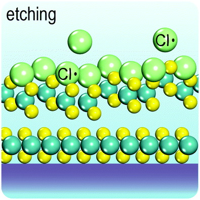
|
N: single/few (controllable)
W ∼ 1 μm |
A few nanosheets per several hours (low) |
✓ Can also produce quantum dots & nanomesh
✗ Highly oxidizing gas is required ✗ High surface roughness ✗ Shrinkage of lateral flake size ✗ Fewlayer nanosheets are required as starting material |
– Transistor
– Fundamental research – HER – Biomedicine |
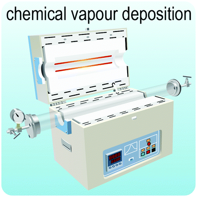
|
N: single/few (controllable)
W: up to wafer scale |
1 Large nanosheet per hour
∼0.1 mg h−1 (moderate) |
✓ Can also produce fullerene-like nanoparticles and nanotubes
✓ Industrially scalable ✓ Large flake size up to wafer scale ✓ Capability of epitaxial growth and alloying ✓ Control over the orientation of deposited nanosheets relative to the substrate ✗ Domain crystalline grain size below 1 μm |
– Transistor
– HER – HDS – Solar cell – Supercapacitor |

|
N: single/few (controllable)
W: up to wafer scale |
One large nanosheet per hour
∼0.1 mg h−1 (moderate) |
✓ Industrially scalable
✓ Low working temperature ✓ Control over the orientation of deposited nanosheets relative to the substrate ✓ Deposition with the correct stoichiometric ratio ✗ Requires high vacuum ✗ Domain crystalline grain size of ∼5–10 nm |
– Transistor
– Photodetector – Solar cell – HER |

|
N: single/few (controllable)
W ∼ 1 cm |
A few large nanosheets per hour
∼10–4 mg h−1 (moderate) |
✓ Can also produce fullerene-like nanoparticles and nanotubes
✓ Capability of epitaxial growth ✗ Expensive and sophisticated equipment ✗ Requires high vacuum |
– (Photo)transistor
– Flexible electronics – Saturable absorber |

|
N: single/few (controllable)
W ∼ 1 μm |
A large number of nanosheets per hour
∼0.01 mg h−1 (moderate) |
✓ Can also produce fullerene-like nanoparticles and nanotubes
✓ Industrially scalable ✓ High optical quality ✓ Magnetic properties can be tailored ✓ Possibility of alloying ✗ Antisite defects are present |
– (Photo)transistor
– Photodetector – Valleytronics |

|
N: 3–5 L
W < 200 nm |
∼ 1 mg h−1 (high) |
✓ Can also produce quantum dots, fullerene-like nanoparticles, nanotubes, nanoflowers and mesoporous structures
✓ Industrially scalable ✓ Widely accessible ✗ Lack of isolated nanosheets |
– Li-ion battery
– HER – PEC water splitting – Supercapacitor – Biomedicine – Hydrogen storage – Superlubricant |

|
N: 1–5 L
W < 100 nm |
∼1 mg h−1 (high) |
✓ Can also produce quantum dots and nanoflowers
✓ Possibility of phase engineering (1T and 2H) ✓ Widely accessible ✓ Possibility of alloying ✗ Need for a high boiling point solvent and an inert atmosphere |
– Li-ion battery
– HER – Biomedicine – Flexible electronics |

|
N: 3-6 L
W ∼ 1 cm |
1 Large nanosheet per hour
∼0.1 mg h−1 (moderate) |
✓ Industrially scalable
✓ Easy to implement ✗ High temperature ✗ Two-step annealing is required |
– Li-ion battery
– Solar cell – (Photo)transistor – HER – PEC water splitting |
The remaining part of this section is devoted to a brief discussion of various technological applications of G6-TMDs and appropriate production methods for each application. For this purpose, we have categorized all reported applications of G6-TMD nanomaterials into five main areas, based on the structural and functional features of the nanomaterials needed by each application. The pertinent subsections are (opto)electronics, sensors, energy storage, catalysis and emerging applications. Each subsection is organized in such a way that first the basic concepts and common principles of the mentioned applications in that subsection are briefly introduced. Then, potential and utilized production methods for these applications are discussed in detail. Finally, in the context of production methods the current challenges faced by the applications in each subsection are critically analysed and possible solutions and pathways for future research are outlined.
6.1. (Opto)electronics
(Opto)electronics has been the most active area of applications of G6-TMDs, over the last decade. Since the silicon-based semiconductors have reached their fundamental performance limits and there is high demand from the electronics industry with a more than $330 billion market726 to find new materials with higher performance and/or larger die size, essential to fabricate faster devices with lower power consumption, numerous research efforts have been made on newly discovered 2D materials. G6-TMDs, especially MoS2 and WSe2, have a leading role along with graphene at the frontier, while they are more promising than graphene in many areas due to their appropriate bandgap, a property which is absent in graphene. Thousands of research articles on (opto)electronic applications of G6-TMDs since 2004 and several yearly specific review papers on their electronic device applications34,124,218,727–731 show the potential and promise in this field of research. Fig. 26 depicts a rainbow of some applications of various G6-TMDs produced with different methods to give an idea of what they can offer and contribute to competitive and mature (opto)electronic technology. | ||
| Fig. 26 A rainbow of (opto)electronics-related applications of various G6-TMDs produced with different methods. Reproduced with permission from: (a) ref. 9. Copyright 2011 Nature Publishing Group; (b) ref. 740. Copyright 2012 American Chemical Society; (c) ref. 192. Copyright 2015, American Association for the Advancement of Science; (d) ref. 778. Copyright 2015 American Chemical Society; (e) ref. 786. Copyright 2015 American Chemical Society; (f) ref. 797. Copyright 2015 Nature Publishing Group; (g) ref. 805. Copyright 2014 Nature Publishing Group; (h) ref. 814. Copyright 2014 Nature Publishing Group; (i) ref. 819. Copyright 2013 American Chemical Society; (j) ref. 46. Copyright 2015 Wiley-VCH; (k) ref. 837. Copyright 2014 American Chemical Society; (l) ref. 838. Copyright 2016 Wiley. Data in panel (m) are extracted and compiled from a set of 408 (opto)electronics-related articles in a database of top 1000 most cited articles with any of the G6-TMD nanomaterials in their topic, based on Web of Science. | ||
000 cm2 V−1 s−1 for graphene by Novoselov et al.6 stimulated great interest in finding an ultimate solution to ultra-fast transistors, soon after it was realised that the absence of bandgap in graphene is a major barrier to utilize it in field effect transistors (FETs) for digital applications.732,733 In fact, graphene FET devices cannot be effectively switched off and the drain and source terminals are always short-circuited, causing high power consumption.
In such a context, a MoS2 based transistor, whose mobility was initially measured by Novoselov et al.7 to be very low, in the range of 0.5–3 cm2 V−1 s−1, came to the forefront, benefiting from an appropriate bandgap of 1.9 eV (single layer), which could guarantee the off-state of the transistor to be really off, and a breakthrough of Kis’ group9 in using HfO2, a material with a high dielectric constant, in a top-gated configuration FET to enhance the electron mobility of the MoS2 channel by dielectric screening (Fig. 26a). Although there was some overestimation on the exact enhancement of the mobility,734,735 which will be discussed in more detail later, there is no debate that the work of Kis’ group injected fresh blood into the research field of 2D materials for electronic devices, especially G6-TMDs.
While micromechanical cleavage has been the main production method of MoS2 nanosheets to fabricate transistors in fundamental research and prototyping, due to its inherent randomness and limitations in scalability, search for alternative production methods has always been an active field. The most likely candidate for rapid and large scale production of electronic-grade MoS2 nanosheets in a controlled manner is CVD which was developed by several groups503,543,548 immediately after the demonstration of the first MoS2 transistor in 2011. So far, transistors based on high quality flakes synthesized by the highly optimized CVD method,736 ambient-pressure CVD (APCVD) on various surfaces,587 metal–organic CVD (MOCVD) with high electron mobility monolayer films508 and epitaxial growth on epi-ready c-plane (0001) sapphire substrate251 have been demonstrated. The CVD method with controllability on size (up to wafer scale) and thickness (monolayer, bilayer and trilayer) by oxygen plasma treatment of SiO2 substrates prior to deposition has also been reported and successfully employed for the fabrication of transistors.737 The main concern in CVD growth of MoS2 nanosheets is the grain boundaries and by controlling the nucleation533 or by using ultraclean substrates without seeds to nucleate growth,183 large area single crystalline nanosheets with high electrical and optical quality comparable to micromechanically exfoliated samples are obtained. Other production methods including liquid phase exfoliation,738 lithium intercalation and exfoliation,454 laser thinning191 and thermal decomposition700 are also used in the fabrication of MoS2 based transistors. Among these methods, thermal decomposition seems to be the most promising and can be the competitor of conventional CVD, thanks to its homogeneous coverage of a large area237 and relatively good mobility of the final film if annealed in an Ar/S atmosphere.700 However, it should be noted that the produced MoS2 samples by thermal decomposition are generally bilayer or trilayer films, and further optimization to produce homogeneous monolayer films still needs to be done. Recent studies on the thickness-dependent mobility of MoS2 transistors revealed that the mobility of transistors based on monolayer MoS2 nanosheets is significantly higher than those based on bilayer and trilayer nanosheets if atmospheric adsorbates are avoided.739
After the successful demonstration of MoS2 transistors, other members of G6-TMDs also garnered attention for digital applications. While transistors fabricated with micromechanically exfoliated MoS2 nanosheets, placed on SiO2/Si substrates with Au contacts, show n-type behaviour,9 the Javey group740 has shown that transistors with monolayer WSe2 as the active channel and Pd or Pd/Au contacts can be doped reversibly with NO2 chemisorption (strong electron acceptor) to attain p-type behaviour with high hole mobility and high performance (Fig. 26b). This group later has also reported WSe2 n-FETs by potassium (K) vapour doping (strong electron donor) and with Au contacts.741 Furthermore, transistors based on MoSe2 nanosheets by micromechanical cleavage742,743 or CVD,243,550 MoTe2 nanosheets by micromechanical cleavage744 and WS2 nanosheets by micromechanical cleavage,745,746 liquid phase exfoliation747 and CVD549 have been fabricated and thoroughly characterized. Among G6-TMD nanostructures other than nanosheets, WS2 nanotubes are also interesting for transistor applications and have their own place and importance.748
A major current trend in G6-TMD transistors is the control over the channel type (n-type and/or p-type), essential for complementary metal-oxide-semiconductor (CMOS) technology and constructing advanced integrated circuits. Micromechanically exfoliated MoS2 nanosheets on SiO2/Si substrates commonly show n-type while WSe2 nanosheets on SiO2/Si usually exhibit p-type characteristics.728,749 However, an ab initio study of the origin of n-type and p-type behaviour of MoS2 monolayers on SiO2 predicted that a defect-free ultra-clean SiO2 substrate plays an insignificant role in the type of conductivity of MoS2, since the valence band maximum (VBM) and conduction band minimum (CBM) of MoS2 are located almost in the middle of the wide bandgap of SiO2 and accordingly SiO2 in contact with MoS2 does not affect the Fermi level of MoS2 toward n- or p-type conductivity.750 Common n-type behaviour of MoS2 nanosheets on a SiO2 substrate is thus attributed to the presence of defects, adsorbates and interface impurities. In agreement to this computational study, ambipolar behaviour of MoS2 on a PMMA substrate has been demonstrated.751 Chemical doping with AuCl3752 or plasma-induced doping during reactive ion etching (RIE) by SF6753 is also used for the fabrication of p-type MoS2 FETs. Furthermore, controlled n- and p-doping with various molecular reductants and oxidants has been reported.517 Another approach to alter the intrinsic conduction of G6-TMD nanosheets is based on the utilization of transistors with different architectures from conventional FETs, such as electric double-layer transistors (EDLTs) or dual top-gated FETs. Ambipolar MoS2 EDLTs by ionic liquids754 and unipolar p-type MoS2 EDLTs by polymer electrolytes755 have been fabricated. WSe2 ambipolar EDLTs with both high electron and hole mobility have also been reported.756 Ambipolar MoTe2 EDLTs757 and MoTe2 dual top-gated transistors758 have been demonstrated, too. Metal contact engineering for controlling the channel type is another important and promising technique, which is also capable of reducing the Schottky barrier height at the interface of the 2D nanosheet and external circuitry towards low-resistance ohmic contacts. In general, high work function materials such as Pd (∼5.1 eV)759 and MoOxx < 3 (∼6.6 eV)760,761 in contact with MoS2 can be used as hole injectors because their Fermi levels lie near or lower than the valence band maximum of MoS2 and thus p-FET devices can be achieved. On the other hand, low work function metals such as In (∼4.1 eV) and Ag (∼4.3 eV) have been used to make WSe2 n-FET devices.762 The effect of various metal contacts to MoS2 and WSe2 nanosheets has been extensively studied763–766 and recently reviewed.767
A unique and interesting property of G6-TMD semiconductors, which can be effectively used to fabricate transistors with high mobility, is the possibility of controlled phase change to metallic phase in contact regions. Fig. 26c shows a representative example of such intelligent local phase patterning in MoTe2 transistors from semiconducting hexagonal (2H) to stable metallic monoclinic (1T′) at the junction of source and drain with Au electrodes, by laser induced Te vacancies.192 The Ohmic contacts between Au electrodes and metallic 1T′-MoTe2 boosts the mobility of the transistor by a factor of 50, while a high on/off ratio of 106 can also be achieved due to the semiconducting nature of the conducting channel. A similar phase engineering strategy by n-BuLi treatment has also been applied to WSe2 nanosheets to fabricate transistors with substantially improved performance with high mobilities of up to 66 cm2 V−1 s−1 and on/off ratios of 107.768
The first voltage amplifier based on monolayer MoS2 FET was fabricated by Kis’ group in 2012, with a gain of 4 for small frequencies (30 Hz) and an above-unity gain for frequencies up to 2 kHz.775 In 2014, two groups reported the fabrication of MoS2 RF FETs operating at GHz frequencies. Krasnozhon et al.,776 by micromechanically exfoliated monolayer and trilayer MoS2 nanosheets in a top-gated FET configuration with a 240 nm gate length, achieved the maximum frequency of oscillation of fmax = 8.2 GHz (fmax is the highest frequency at which a transistor can still amplify the power of an input signal). Cheng et al.777 also reported the fabrication of fewlayer MoS2 FETs on rigid and flexible substrates, with record fmax = 50 GHz in a 68 nm channel length device. Another important step in RF applications of MoS2 was taken by Sanne et al.778 who fabricated CVD grown MoS2 FETs by sulfurization of MoO3 with fmax = 5.3 GHz at a gate length of 250 nm (Fig. 26d). Recently, Krasnozhon et al.779 have investigated the effect of channel length scaling on the RF performance of MoS2 transistors and found that fT and fmax of trilayer MoS2 RF FETs obey the typical monotonic modulation by the inverse of gate length down to 40 nm and fabricated a transistor with fmax = 16 GHz at this low gate length. Evaluation of other production methods, especially those developed and highly optimized in recent years, such as liquid phase exfoliation, MOCVD, epitaxial growth on an appropriate substrate, PVD techniques and thermal decomposition as well as assessment of other potential members of G6-TMDs beyond MoS2, in particular WSe2, are promising research topics in 2D RF FETs which still have remained untouched.
While aforementioned inverters were based on micromechanically exfoliated flakes, an NMOS inverter based on CVD grown monolayer MoS2 with a voltage gain of higher than 12785 and a resistor-loaded inverter based on CVD grown monolayer WSe2 with a voltage gain of about 13149 have been reported. An interesting CMOS invertor has also been proposed by Duan's group527 based on a lateral heterojunction of WS2 as nFET at the centre and WSe2 as pFET in the peripheral regions of a CVD grown triangular domain, with voltage gain of 24. Recently, Jeon et al.786 have employed intrinsically n-MoS2 (5.4 nm) with Ti metal contacts and p-WSe2 (3.5 nm) with Pt metal contacts on glass substrates and a fluoropolymer CYTOP passivation layer coating to fabricate a CMOS inverter and obtained a maximum voltage gain of 27 and sub-nanowatt power consumption (Fig. 26e). They also demonstrated other hetero-CMOS logic gates such as OR, NOT and AND gates by using n-MoS2 and p-WSe2. Last, but not the least, a three-level multivalued logic circuit from the MoS2/WSe2 heterojunction has been demonstrated very recently by Nourbakhsh et al.787
Saturable absorption is a nonlinear optical property (NLO) of certain materials and occurs when the intensity of incident light to the material exceeds above a threshold (but still below the optical damage) and saturation of excited electrons in the conduction band causes a sudden fall in absorption of the material by some percent (modulation depth) which makes the material relatively transparent to excess light. G6-TMDs exhibit ultrafast broadband saturable absorption from visible to near IR with a typically 0.5–100 GW cm−2 saturation intensity and corresponding modulation depth of 1–30%.147,795–797 NLO properties of G6-TMDs including nonlinear refraction and nonlinear absorption coefficients have been extensively studied by the Z-scan technique.147,384 One of the main applications of saturable absorbers is in fibre lasers for generation of high energetic and short duration pulses. There are two basic techniques, namely Q-switching for high-energy (μJ–mJ) and short duration (ns–μs) pulses with moderate repetition frequency (kHz) and mode-locking for moderate-energy (pJ–μJ) and very short duration (fs–ps) pulses with high repetition frequency (MHz–GHz).798 Chen et al.796 prepared solutions of MoS2, MoSe2, WS2 and WSe2 nanosheets in water by the surfactant assisted liquid phase exfoliation method and subsequently embedded nanosheets in a transparent polymer, polyvinyl alcohol (PVA), and found that with a similar preparation method, MoSe2 nanocomposites show the highest modulation depth while WS2 nanocomposites exhibit a more stable train of pulses in a Q-switched fiber laser. Luo et al.157 also demonstrated an all-fiber pulsed laser in visible wavelengths (red) by the Q-switching technique based on liquid phase exfoliated MoS2, MoSe2 and WS2 few layer nanosheets as the saturable absorber. Several mode-locked fiber lasers have been demonstrated based on G6-TMDs, too.795,797,799,800 For example, Mao et al.797 prepared a solution of WS2 nanosheets in water/ethanol by sonication and centrifugation and fabricated two mode-locked pulsed laser systems, one based on deposition of the solution onto a D-shaped fiber and another by coating of the facet of the fiber connector inside the laser cavity with a WS2/PVA nanocomposite (Fig. 26f). They obtained stable ultrafast mode-locked pulses even when the pump power was increased to 600 mW, with the shortest duration time of 1.32 ps for the D-shaped fiber and 1.2 ps for the WS2-PVA film. Although liquid phase exfoliation is the preferred method for fabricating saturable absorbers based on G6-TMDs, other fabrication methods such as lithium intercalation,795 pulsed laser deposition624,800 and chemical vapour deposition799 have been successfully employed.
Electroluminescence and Light emitting diodes (LED) based on G6-TMDs have attracted considerable attention in recent years, largely due to the direct bandgap of their monolayers. Initial reports of strong electroluminescence at ∼1.8 eV for monolayer MoS2801 and ∼2.0 eV for monolayer WS2802 have provided great impetus for a more intense study to fabricate LEDs from this family of materials. The building block of conventional LEDs is a p–n junction in which injected electrons and holes into the device from electrodes combine radiatively. A vertical p–n junction from an intrinsic n-MoS2 nanosheet and a p-type Si substrate has been demonstrated with a threshold power of 3.2 W cm−2.803 A lateral p–n junction through electrostatic doping of two different regions of monolayer WSe2 by two distinct gates (one with a positive and another with a negative bias voltage) has been also demonstrated.804,805 WSe2 based LEDs show high optical quality and bright electroluminescence with 10 times smaller linewidth than the MoS2/Si LED and are 1000 times more efficient in terms of injection current (Fig. 26g).805 As an alternative route to LEDs based on p–n junctions, quantum wells with a van der Waals heterostructure of Gr/hBN/TMD/hBN/Gr, in which hBN layers act as tunnel barriers and graphene flakes serve as transparent electrodes, have been also proposed for low-power light emitting diodes.299,806 It was shown that while MoX2 (X = S, Se) light emitting quantum wells (LEQWs) have good performance at cryogenic temperatures, W-based ones, and more specifically WSe2 LEQWs, have at least 250 times better external quantum efficiency at room temperature, due to the dark state of the lowest-energy exciton in W-based G6-TMDs.299
Fig. 26i shows the transfer curve of a leading work by Kis’ group819 that has demonstrated non-volatile flash memory based on a monolayer MoS2 nanosheet as the active channel and graphene as the charge trapping floating gate. The fabricated memory cell, exhibited good performance with 104 program/erase current ratio and a memory window of about 8 V which ensures very slow charge leakage from the floating gate and the retention time on the time-scale of years. This work was pursued by many other research groups and for example it was shown that replacing the multilayer graphene floating gate by a HfO2 charge trap layer increases the memory window up to 20 V with only 28% charge loss of the floating gate after 10 years, a very stable retention characteristic.820 A systematic computational study of flash memory devices based on MoS2, MoSe2, WS2 and WSe2 as the active channel with graphene floating gate predicted the great potential of G6-TMDs, especially WSe2, to surpass Si-based technology for future sub-10 nm node memory cells.821 A DRAM based on micromechanically exfoliated fewlayer MoS2 has also been fabricated recently with a very low current leakage (1.7 × 10⁻¹⁵ A μm−1) thanks to the wide bandgap and high electron effective mass of MoS2.822 A photoresponsive non-volatile rewritable memory device based on graphene-MoS2 hybrid has also been demonstrated, in which a red LED was employed to program data and gate voltage pulses to erase them.823
Apart from micromechanical cleavage, other production methods are also widely used to prepare various G6-TMD nanostructures for memory devices. The leading research group of Zhang has demonstrated several non-volatile flash memory devices including a composite of MoS2 nanosheets and PVP (polyvinylpyrrolidone) as an active layer prepared by sonication and exfoliation sandwiched between Al and rGO electrodes,376 a MoS2 and graphene oxide mixture as an active layer prepared by electrochemical lithium intercalation and exfoliation with Al and ITO electrodes824 and an active layer of chiral MoS2 nanofibersbetween rGO electrodes on a flexible PET (polyethylene terephthalate) substrate.71 The same group has also fabricated DRAM from MoS2 nanobelts decorated with noble metal particles, such as Pt or PtAg alloy, composited with PVP as an active layer between Al and ITO.63 Interestingly, non-volatile write-once-read-many (WORM) memory devices by quantum dots of TMDs including MoS2, MoSe2, WS2 and WSe2, prepared by grinding/sonication and composited with PVP have been demonstrated by the Zhang group.46 The best-performing device with an Au/MoS2–PVP/ITO structure (Fig. 26j) had 4 × 10⁵ program/erase current ratio and showed long retention time.
The discussion on memory devices will not be complete unless we mention memristors based on G6-TMDs, a rather new research topic, which has stimulated considerable interest. A memristor is conceptually the fourth circuit element with two terminals, along with other three resistor, capacitor and inductor two-terminal elements, which directly relates the electrical charge and magnetic flux.825 A memristor was theoretically predicted and postulated by Chua825,826 in the 1970s and demonstrated experimentally for the first time in 2009 by a group of researchers at HP corporation in a Pt/TiO2−x/Pt (metal/insulator/metal) stack.827 There are some debates that whether any resistance switching memory is a memristor828 or these memory devices, including the one claimed in Pt/TiO2−x/Pt, are based on non-magnetic phenomena and thus are not memristors.829 Waser and coworkers830,831 have reviewed many such devices and classified the possible mechanisms into three thermal, electrical and ion-migration-induced primary types. Many related resistance switching memory phenomena such as charge trapping/detrapping, formation and disruption of conductive filaments and migration of metal cations and oxygen anions were explained in this framework. Nonetheless, Bessonov et al.832 have reported memristive behaviour in solution processed MoOx/MoS2 and WOx/WS2 films when sandwiched between Ag electrodes. The fabricated memristors required only a very low voltage of 0.1–0.2 V to be programmed appealing for low-power applications. Sangwan et al.205 have also demonstrated memristors based on CVD grown monolayer MoS2 nanosheets that had superior controllability on switching voltage in comparison with conventional metal/insulator/metal memristors. They attributed the memristive behaviour to the grain boundaries and investigated the effect of orientations of grain boundaries on the device performance. Recent advances in memory devices based on 2D materials, particularly graphene and G6-TMDs, have been reviewed by Zhang and coworkers.833
In principle, nearly all of the electronic devices discussed in this section can be made flexible and/or transparent. To date, for example, flexible and transparent transistors for digital applications from MoS2839,840 and WS2,841 flexible RF transistors for analog applications based on MoS2,777,842 flexible complementary logic circuit based on MoS2 and WSe2836,843,844 and flexible memory devices based on MoS2376 as well as flexible photovoltaics from WS2788 and flexible photodetectors based on MoS2710 and WSe2845 have been demonstrated. Again, similar to many other electronic applications, micromechanical cleavage is widely used for prototyping and making proof-of-concept flexible/transparent devices while CVD755,842–844 is the prime candidate for mass production. Furthermore, liquid phase exfoliation of MoS2 nanosheets for fabrication of flexible memory devices,376 thermal decomposition for fabrication of MoS2-based flexible photodetectors710 and pulsed laser deposition for fabrication of WSe2-based flexible and transparent photodetectors845 have also been successfully applied. Many research groups have routinely used polyimide755,777,842,843 and PET788,839 as flexible substrates in their devices but when higher transparency or special dielectric properties are desired, PEN,840,846 PMMA751 and PDMS847 are also used.
Das et al.837 fabricated an all-2D flexible and transparent thin film transistor from a bilayer of WSe2 as the active channel, h-BN as the gate dielectric and graphene as the contact electrodes on a PET substrate (Fig. 26k). Their device exhibited excellent performance with ambipolar characteristic, electron mobility of 34 cm2 V−1 s−1, hole mobility of 45 cm2 V−1 s−1, Ion/Ioff ratio of 107, unaltered behaviour up to 2% mechanical strain and above 88% transparency to visible light. Hong and coworkers838 recently demonstrated a flexible thin film transistor based on multilayer MoS2 with a record mobility of 141 cm2 V−1 s−1 and Ion/Ioff ratio of 5 × 10⁵ with robust behaviour up to 5 mm bending radius (Fig. 26l). In their device the multilayer MoS2 was used as the active channel, while a thin Al2O3 layer on an organic material (SU-8), for better flexibility and adhesion, was used as the gate dielectric. A connected and welded network of Ag nanowires in a polyimide matrix was also used as the gate electrode. At the end, it is worth mentioning that strain engineering in G6-TMDs has been reviewed in detail, recently.301,848 Those readers who are interested in a comprehensive treatment of 2D-based flexible electronics will also appreciate two excellent reviews by Kim et al.849 and Hone and coworkers.835
The last panel of Fig. 26 shows a pie chart that represents the percentage of use of each production method of G6-TMDs in the ∼400 highly cited articles with orientation of (opto)electronics applications. These articles were extracted from a database of top 1000 most cited articles with the G6-TMD nanostructures in their topic based on Web of Science. Careful examination of the chart reveals that the micromechanical cleavage certainly is the first choice for the assessment of ideas and prototyping in (opto)electronics. The successful ideas then have the chance to be realized by two major scalable production methods, chemical vapour deposition (CVD) and liquid phase exfoliation (LPE). In this regard, the CVD method is generally used in transistor related devices while LPE is more appropriate for saturable absorbers and memory devices. Currently the main challenges in the production of G6-TMD nanostructures by CVD for (opto)electronic applications are: (i) the precise control of the number of layers during the growth of nanosheets, (ii) epitaxial growth of films at the wafer scale with large single-crystalline domains and the lowest possible grain boundaries and (iii) growth at lower temperatures towards direct deposition on various substrates other than SiO2/Si, for example ITO, FTO and flexible polymeric substrates. The main directions that should be followed for LPE are (i) further optimization of parameters to increase the yield of monolayer and simultaneously (ii) increase the lateral size of the produced nanosheets at least above 10 μm. Li intercalation due to the inherently unstable nature of the produced 1T phase has received little attention in the field of (opto)electronics; however, there is great potential if (i) an appropriate stabilization method of metallic 1T or (ii) a rapid and efficient transformation method from metallic 1T to 2H semiconducting phase without agglomeration and restacking can be developed. Other methods, including thinning and solution-based methods were not often the focus of researchers in (opto)electronics, but in our opinion, laser thinning, etching and notably thermal decomposition – as a scalable method, have great potential to be employed in many state-of-the-art (opto)electronic devices and thus deserve more attention.
Before concluding the (opto)electronics section, to make the present picture more complete, it would be instructive to review some experimental necessary considerations and required figures of merit of 2D electronics. As is shown in Fig. 27 the first report on single layer MoS2 transistor in 2011 had a systematic underestimation in the measurement of the mobility.9,734,735 In fact, when mobility is measured in double-gated transistors with the top-gate capacitance substantially higher than the back-gate capacitance (i.e. Cbg ≪ Ctg), special attention must be given to appropriately ground the top gate before the mobility measurement using the back gate.734 Simple disconnection of the top gate may result in a field effect mobility an order of magnitude higher than the actual mobility due to capacitive coupling between the top and back gates in this configuration. For a more accurate measurement of electron and hole mobilities a four-probe Hall effect technique should be used.734,850 Thus, many existing reports of high mobilities of G6-TMD transistors (sometimes up to 1000 cm2 V−1 s−1 at room temperature) have had a major overestimation and are not reliable.
 | ||
| Fig. 27 Experimental considerations of two-probe measurement of the field effect mobility in dual-gated transistors. (a) An example of overestimation of mobility in a dual-gated MoS2 transistor when measured using the back gate while the top gate is disconnected. The transfer characteristic curve is plotted by applying a constant drain–source voltage of Vds = 10 mV and measuring the drain–source current (Ids) by sweeping the back gate voltage (Vbg) while the top gate is disconnected instead of being grounded. The mobility can be estimated from the linear region of the plot knowing the correct capacitance between the MoS2 channel and the back gate. (b) Effective capacitance between the MoS2 active channel and the Si back gate in two cases when the top gate is simply disconnected or when it is appropriately grounded. Figure adapted with permission from: (a) ref. 9. Copyright 2011 Macmillan Publishers Ltd and (b) ref. 734. Copyright 2013 Macmillan Publishers Ltd. | ||
In Fig. 28 we have summarized mobilities versus Ion/Ioff ratios of the most important reports of G6-TMDs along with other conventional semiconductors, such as polycrystalline silicon (p-Si), amorphous silicon (a-Si), InGaZnO (IGZO) and organic semiconductors as well as other state-of-the-art competitors such as carbon nanotubes, graphene and phosphorene. In the preparation of this plot we did our best to avoid unreliable reports. It is evident from this figure that G6-TMDs like graphene have no chance, at least from a short to medium term perspective, to be employed in high performance transistors as pointed out by other experts.33,726,834,835 However they are very promising for low power and cost effective thin film transistors with medium performance, particularly when flexibility and transparency are desired.834,835
 | ||
| Fig. 28 Mobility vs. on/off current ratio, an important figure of merit for thin film transistors. A higher mobility is desirable for future transistors with higher speed and performance while a higher on/off current ratio is required for lower power consumption. Data are taken from the International Technology Roadmap for Semiconductors (yellow star): ITRS 2.0 low power target for 2021, ref. 851; set of conventional semiconductors (red dots): p-Si, ref. 853; IGZO, ref. 854; a-Si, ref. 855; set of graphene (black squares): Gr1, ref. 856; Gr2, ref. 857; Gr (FL), ref. 6; Gr (2L), ref. 858; set of single-walled carbon nanotube network (grey circles): CNT1, ref. 859; CNT2, ref. 860; set of phosphorene (green rhombi): Ph1, ref. 861; Ph2, ref. 862; Ph3, ref. 863; set of organic semiconductors (orange triangles): organic1 [pentacene, ref. 864 and rubrene, ref. 865]; organic2, P3HT ref. 866; organic3, pentacene, ref. 867; set of group-6 transition metal dichalcogenides (blue spheres): MoS2 (FL, LPE), ref. 738; MoS2 (1L, thin), ref. 191; MoS2 (FL, TD), ref. 700; MoS2 (FL, I&E), ref. 469; TMDs1 [MoS2 (multi-layer, MC), ref. 838; MoSe2 (multi-layer, MC), ref. 742; WSe2 (1L, MC, pFET), ref. 740; WSe2 (1L, MC, nFET), ref. 762]; TMDs2 [MoS2(FL, MC), ref. 219; MoS2 (1L, MOCVD), ref. 508; MoSe2 (1L, CVD), ref. 243; MoTe2 (multi-layer, MC), ref. 192; WS2 (1L, MC), ref. 745; WS2 (1L, MOCVD), ref. 508]; TMDs3 [WSe2 (1L, CVD), ref. 768; WSe2 (FL, MC, flexible), ref. 837]; TMDs4 [MoS2 (1L, MC), ref. 868; WS2 (multilayer, MC), ref. 746]. Acronyms: 1L, monolayer; FL, fewlayer, MC, micromechanical cleavage; LPE, liquid phase exfoliation; I&E, intercalation and exfoliation; thin, thinning; CVD, chemical vapour deposition; TD, thermal decomposition. | ||
It should be noted that according to the International Technology Roadmap for Semiconductors (ITRS 2.0),851 the current 14 nm node technology for high-performance (HP) transistors should be improved to 10 nm node by 2018 and 5 nm node by 2021. From this perspective, G6-TMDs, especially MoS2 and WSe2, are expected to receive increasingly more attention because in such an aggressively reduced feature size the transport of electrons and holes changes from the diffusive regime to the ballistic regime.33,726,834
In the ballistic regime the mobility is a non-relevant concept and low mobility related issues of G6-TMDs are relieved. Instead, the larger bandgap and the higher carrier effective mass of G6-TMDs relative to the conventional semiconductors, such as Si, Ge and GaAs, will become a necessity to avoid the short channel effect and undesired source–drain tunneling at these extremely scaled channel lengths.726,834 Thus along with thin film transistors, high performance tunneling transistors based on G6-TMDs with a sub 10 nm channel length have great promise for future electronics.852
Fiori et al.834 listed several important figures of merit for digital high performance (HP) and digital low power (LP) applications as well as analog applications of 2D materials. In general, Ion/Ioff > 104, mobility in the range of 1–100 cm2 V−1 s−1, subthreshold swing (SS) equal to or smaller than ∼60 mV dec−1 and contact resistance below 130 Ω μm are required. Other criteria including power consumption (PD), operating voltage (VDD), intrinsic delay time (τ) and dynamic power indicator (DPI) have been thoroughly discussed in the above review article. Schwierz et al.33 also presented a wish list of desirable properties of an ideal 2D material as the active channel in a field effect transistor, including recommended (i) bandgap, (ii) carrier transport and effective mass, (iii) heat transport, (iv) contact resistance and (v) scale length and channel thickness. There are many informative charts and comparative tables for both digital high performance transistors and RF transistors in this review article that can guide researchers to concentrate their resources and efforts. Lastly, interested readers are referred to two insightful review articles by Wang et al.727 and Franklin et al.726 as well as a recent comprehensive chapter book by Nichols et al.850 to obtain a more detailed discussion on some other aspects of (opto)electronic applications of G6-TMDs that were not fully covered here.
6.2. Energy storage
Energy storage is one of the most important and relevant application areas of G6-TMD nanomaterials. Inevitable run out of fossil fuels in a few decades ahead and increasing environmental concerns worldwide have shifted global energy policy from oil and gas to renewable energy sources, such as solar and wind energies. However, these types of energies, even at a specific area, generally depend on daytime and seasonal changes; thus energy storage devices become of paramount importance for stabilizing supply of renewable energies at all times and in all places. Several energy conversion/storage devices are under intensive research and development, including fuel cells, batteries, capacitors and supercapacitors.869,870 The two main figures of merit of any energy storage device are the specific energy measured in W h kg−1 and the specific power in W kg−1. Fig. 29a shows a comparison of different technologies for energy storage with respect to these metrics, called the Ragone plot.869,871,872 Fuel cells are of high specific energy and they are intended to replace fossil fuels in heavy industries and electric cars. It is to note that fuel cells are actually energy conversion devices and their inclusion in the Ragone plot should be interpreted with caution in view of the exact definition of the device weight (see ref. 871 for a good discussion of this issue). In energy storage devices, conventional capacitors are of high specific power and can deliver a large amount of energy in a short period of time on the order of milliseconds. Batteries and supercapacitors have also their own place in this plot. Today, commercial batteries can supply a relatively high specific energy of 100–300 W h kg−1 with a typical full charge/discharge cycle of about 1 h but suffer from low specific power of 10–100 W kg−1.870,873 Supercapacitors are a newer technology and developed to fill the gap between high specific energy batteries and high specific power capacitors. Nowadays, supercapacitors are used in electric buses, electric trams, elevators and in digital circuits for the backup of memory devices.874 They store moderate specific energies of 1–10 W h kg−1 and can deliver their energy with a high specific power of 1000 W kg−1. Their charging is also fast within a fraction of a minute and can be charged/discharged more than 100000 cycles without any obvious capacity decay.870,875
 | ||
| Fig. 29 Application of G6-TMD nanomaterials in the field of energy storage. (a) Ragone plot of various energy conversion/storage devices in terms of their specific energy, specific power and the characteristic running time at the nominal power. The U.S. Department of Energy (DOE) 2022 targets for batteries and supercapacitors are also marked by yellow stars. (b) Schematic illustration of the basic working mechanism of a lithium-ion battery. (c) Schematic illustration of the main capacitive energy storage mechanisms in supercapacitors. (d) Characteristic cyclic voltammograms (CV) of the four types of energy storage devices. (e–g) Electrochemical characterization of a representative battery based on a MoS2-coated 3D graphene network (MoS2/3DGN) as the working electrode and a Li foil as the counter electrode. (e) CV of the MoS2/3DGN electrode at a scan rate of 0.5 mV s−1. (f) The first three charge and discharge curves of the MoS2/3DGN electrode at a current density of 100 mA g−1. (g) Cycling stability behaviour of the MoS2/3DGN electrode. (h and i) Electrochemical characterization of a representative supercapacitor based on restacked 1T-MoS2 nanosheets. (h) CV curves of 1T-MoS2 electrodes at a scan rate of 20 mV s−1 in 0.5 M K2SO4 and 1 M KCl. (i) Galvanostatic charge/discharge curves of 1T-MoS2 electrodes in 1 M K2SO4. (j) A pie chart showing the percentage of each major production route of G6-TMDs in fabricated energy storage devices, extracted and compiled from a set of 156 energy-related articles in a database of top 1000 most cited articles with any of the G6-TMD nanomaterials in their topic, based on Web of Science. Figure adapted with permission from: (a) ref. 872. Copyright 2014 Wiley-VCH; DOE 2022 targets are from ref. 870, 896 and 897; (b) ref. 878. Copyright 2013 American Chemical Society; (c) ref. 895. Copyright 2014 American Association for the Advancement of Science; (d) ref. 894. Copyright 2016 Nature Publishing Group; (e–g) ref. 898. Copyright 2013 Wiley-VCH; (h and i) ref. 444. Copyright 2015 Macmillan Publishers Ltd. | ||
G6-TMD nanomaterials have clear advantages in energy storage applications, including: (i) high available specific surface area, (ii) abundance of active reaction sites at edges and defects, (iii) low intercalation barrier for various cations, (iv) short diffusion path lengths for ions, (v) very rich morphologies and polytypes, (vi) high chemical stability, (vii) lightness and (viii) good flexibility and mechanical stability. The main challenges that should be overcome before the full potential of G6-TMDs can be realized in the field of energy storage are (i) their intrinsic low electrical conductivity and (ii) electrode destruction and pulverization during repetitive intercalation/deintercalation cycles. Research studies for employing G6-TMD advantages in energy storage devices can be divided into two major research fields of batteries and supercapacitors.
Different types of batteries with different specific energy and power densities are available, such as lead–acid, nickel–cadmium, nickel–metal hydride, lithium-ion, sodium-ion, lithium–oxygen, lithium–sulfur and magnesium batteries. Among the aforementioned battery types, lithium-ion batteries (LIBs) exhibited the most promising performance and are now ubiquitously used in many portable consumer devices, such as laptops and smart phones.876Fig. 29b shows the basic working mechanism of Li-ion batteries. During the charge cycle, lithium ions are expelled from the cathode (commonly LiCoO2) and are intercalated in a layered anode material (commonly graphite) through a lithium conducting electrolyte (commonly, LiPF6, LiBF4 or LiClO4 salts dissolved in a mixture of ethylene carbonate with alkyl carbonate solvents, such as dimethyl carbonate, diethyl carbonate or ethylmethyl carbonate) by applying an external voltage.877–882 In the discharge cycle Li+ ions are deintercalated from the anode and are inserted again in the cathode. While some attempts have been made to employ G6-TMDs as the cathode for replacing LiCoO2,883,884 it seems that they cannot compete with LiCoO2, at least in terms of cathodic voltage.885 However, the higher theoretical specific capacity of G6-TMDs compared with graphite is very promising to employ them as the anode electrode in Li-ion batteries. In fact, while the theoretical specific capacity of graphite is 372 mA h g−1,886,887 it is 670 mA h g−1 for MoS2,69,888,889 422 mA h g−1 for MoSe2,890 and 433 mA h g−1 for WS2.242,891,892
G6-TMDs are also very attractive for replacing conventional activated carbon electrodes in supercapacitors. Fig. 29c shows the working principle of a supercapacitor. The capacitance of a supercapacitor is composed of two main portions. The first portion, called the electrical double layer, is based on electrostatic storage of ions at the surface of electrodes (in a thin layer called the Helmholtz double layer) and the second portion, called pseudocapacitance, is due to the electrochemical storage of charged species through surface redox or intercalation mechanisms.872 Supercapacitors in which the electrical double layer mechanism is dominant are very fast (high specific power) but have a lower capacity for charge storage (low specific energy) compared with those supercapacitors that rely primarily on pseudocapacitance which is a slower process but of much higher capacity.893 Obviously, G6-TMD nanomaterials, due to their high specific surface area and potential for intercalation, exhibit high electrical double layer capacitance and pseudocapacitance and thus are encouraging candidates for supercapacitor electrodes.
One of the key characterization techniques of energy storage devices is cyclic voltammogram (CV) in which the voltage is swiped linearly and the current is recorded.894 CV provides a powerful tool to distinguish between different charge storage mechanisms involved in the device (Fig. 29d). Batteries exhibit two or more paired anodic and cathodic peaks separated from each other by at least 0.1 V.895 Ideal capacitors, on the other hand, have rectangular CV curves. For supercapacitors also the redox-based or intercalation-based mechanisms of the charge storage can be distinguished from the CV curve as elucidated in Fig. 29d. In the following we discuss the application of G6-TMDs in batteries and supercapacitors through several illustrative examples and highlight important strategies to improve the performance of fabricated devices with an emphasis on various available production methods for G6-TMDs.
| MoS2 + xLi+ + xe− → LixMoS2 | (20) |
| MoS2 + 4Li+ + 4e− → 2Li2S + Mo | (21) |
Eqn (20) implies the partial lithiation of MoS2 and transformation from the semiconducting 2H-MoS2 polytype (trigonal) into the metallic 1T-MoS2 polytype (octahedral) with a distinct peak usually observed around 1.2 V (vs. Li/Li+);665 however, depending on the specific electrode composition other values, such as 1.4 V and 0.9 V, have also been reported.898,901–903 The second equation, eqn (21), describes the complete conversion of MoS2 into metallic Mo nanoclusters embedded in a Li2S matrix with a finger print at 0.6 V.665,898–900 Accordingly, sometimes the above two reactions are called intercalation (transition) and conversion, respectively.665,899 Lithium insertion into defects or expanded space of the MoS2 interlayer may add a shoulder of higher voltages (∼0.79 V)900 to the conversion peak (∼0.6 V), whereas irreversible formation of a gel-like solid electrolyte interface (SEI) shifts and broadens the conversion peak to the lower voltage values.665,901 After the lithiation process, in the delithiation sweep, again two peaks can be detected; one weak peak around 1.7 V attributed to the oxidation of Mo particles into MoS2:899
| Mo + 2Li2S → MoS2 + 4Li+ + 4e− | (22) |
| Li2S → 2Li+ + S + 2e− | (23) |
It is proposed that the oxidation of Mo particles can be separated into two processes of Mo → Mo4+ around 1.47 V and Mo4+ → Mo6+ around 1.74 V.903 After the first discharge/charge cycle is completed, the cathodic branch is considerably changed. The conversion peak around 0.6 V described by eqn (21) disappears and a new peak at about 1.9 V emerges due to the conversion of elemental sulfur (S8) to other polysulfides and eventually into Li2S according to the following equation:899,900
| S + 2Li+ + 2e− → Li2S | (24) |
It should be noted that after the first cycle, MoS2 is transformed into dissociated Mo and S atoms and the initial perfect MoS2 crystal structure is not recovered again.665,902
Some representative and distinguished works on batteries based on G6-TMD nanomaterials are summarized in Table 9. A variety of morphologies have been synthesized by various production methods to fabricate batteries of higher performance.876,891,898 The main figure of merit to compare different batteries is the reversible capacity (measured in mA h g−1), which is the capacity of the battery after several charge/discharge cycles (routinely above 50 cycles) at intermediate current densities (routinely 100 mA g−1) when the performance of the battery becomes stable and the ratio of discharge to charge capacities (Coulombic efficiency) approaches unity. First cycle capacities are also included in Table 9 to give an estimation of the highest possible specific capacities of the listed electrodes. This capacity fades upon cycling, primarily due to electrolyte decomposition at the surface of electrodes, formation of a SEI passivation layer and trapping of Li+ ions between G6-TMD layers during the first cycles.888,891 Another key metric in comparison of batteries is the reversible capacity (after several cycles) at high current densities (usually above 1 A g−1) which determines the rate capability, the ability of a battery for fast charging and delivering energy at high power levels. For near future, batteries with an energy density of at least 250 W h kg−1 and a cyclability of over 5000 are targeted.870
| # | Nanomateriala | Production method (MX2) | Battery typeb | Cycling performance | Rate performance | Ref. | |||
|---|---|---|---|---|---|---|---|---|---|
| First cycle capacityc (mA h g−1) | Reversible capacityd (mA h g−1) | Current (mA g−1) | Capacity (mA h g−1) | Current (A g−1) | |||||
| a Reduced graphene oxide (rGO), nitrogen-doped rGO (NrGO), graphene (Gr), carbon nanofibres (CNF), single-walled carbon nanotubes (SWCNT), multi-walled carbon nanotubes (MWCNT), polyaniline (PANI), amorphous carbon (a-C), N-doped carbon (N-C), poly(ethylene oxide) (PEO). b Lithium-ion battery (LIB), sodium-ion battery (SIB), magnesium battery (Mg), lithium–sulfur battery (Li–S). c Discharge (D), charge (C). d Reversible capacity after # cycles. | |||||||||
| 1 | MoS2 hollow nanospheres | Solvothermal | LIB | 1508(D)/1270(C) | 1100 (#100) | 500 | 576 | 5 | 904 |
| 2 | MoS2 nanoplates | Solvothermal | LIB | 1062(D)/917(C) | 907 (#50) | 1062 | 554 | 53.1 | 906 |
| 3 | MoS2 microboxes | Hydrothermal | LIB | 1080(D)/830(C) | 900 (#50) | 100 | 700 | 1 | 69 |
| 4 | Mesoporous MoS2 | CVD | LIB | 1052(D)/— | 876 (#100) | 100 | 608 | 10 | 905 |
| 5 | MoS2 tubular architectures | Solvothermal | LIB | 1172(D)/800(C) | 839 (#50) | 100 | 500 | 5 | 678 |
| 6 | Restacked MoS2 | Intercalation | LIB | — | 750 (#50) | 50 | 710 | 1 | 907 |
| 7 | MoS2 microspheres | Hydrothermal | LIB | 1160(D)/791(C) | 672 (#50) | 100 | 353 | 1 | 908 |
| 8 | MoS2/rGO composite | Hydrothermal | LIB | 2200(D)/1300(C) | 1290 (#50) | 100 | 1040 | 1 | 665 |
| 9 | 3D MoS2–rGO architecture | Sonication | LIB | 1550(D)/1220(C) | 1216 (#30) | 74 | 711 | 1.86 | 414 |
| 10 | MoS2–NrGO film | Hydrothermal | LIB | 1181(D)/1875(C) | 1205 (#200) | 100 | 710 | 5 | 909 |
| 11 | MoS2/rGO composite | Hydrothermal | LIB | 1571(D)/1031(C) | 1187 (#100) | 100 | 900 | 1 | 666 |
| 12 | 3D-MoS2/3D-Gr-foam | Hydrothermal | LIB | 1158(D)/1397(C) | 1100 (#40) | 100 | 800 | 5 | 910 |
| 13 | MoS2⊥rGO heterostructures | Hydrothermal | LIB | 1160(D)/896(C) | 1077 (#150) | 100 | 907 | 1 | 911 |
| 14 | MoS2/3D-Gr-network | Thermolysis | LIB | 1222(D)/1020(C) | 877 (#50) | 100 | 597 | 1 | 898 |
| 15 | WS2/rGO composite | Sonication | LIB | 1034(D)/500(C) | 451 (#50) | 100 | 179 | 4 | 912 |
| 16 | CNF@MoS2 | Hydrothermal | LIB | 1489(D)/983(C) | 1264 (#50) | 100 | 688 | 1 | 903 |
| 17 | MoS2/SWCNT composite | Sonication | LIB | 1350(D)/1281(C) | 1215 (#50) | 100 | 600 | 20 | 913 |
| 18 | MWCNT@MoS2 | Solvothermal | LIB | 1350(D)/973(C) | 1027 (#200) | 50 | 610 | 0.25 | 914 |
| 19 | MoS2-CNF composite | Thermolysis | LIB | 1712(D)/1267(C) | 1007 (#100@1 A g−1) | 100 | 374 | 50 | 915 |
| 20 | MoS2/PANI-nanowires | Hydrothermal | LIB | 1450(D)/1063(C) | 953 (#50) | 100 | 320 | 1 | 916 |
| 21 | MoS2/TiO2-nanowires | Hydrothermal | LIB | 862(D)/724(C) | 544 (#100) | 100 | 414 | 1 | 917 |
| 22 | MoS2/a-C composite | Hydrothermal | LIB | 2070(D)/926(C) | 912 (#100) | 100 | — | — | 918 |
| 23 | C/MoS2-nanoflowers | Hydrothermal | LIB | 1419(D)/988(C) | 837 (#50) | 100 | 672 | 10 | 901 |
| 24 | MoSe2/a-C composite | Hydrothermal | LIB | 822(D)/594(C) | 577 (#50) | 100 | 450 | 2 | 919 |
| 25 | Ag/Fe3O4–MoS2 | Sonication | LIB | 1624(D)/1286(C) | 1233 (#100) | 200 | 1026 | 1 | 920 |
| 26 | MoSe2/hollow-carbon-sphere | Hydrothermal | SIB | 840(D)/560(C) | 580 (#100) | 200 | 400 | 1.5 | 921 |
| 27 | Vertical-Gr/MoSe2/N-C | Hydrothermal | SIB | 786(D)/535(C) | 534 (#400) | 200 | 298 | 2 | 922 |
| 28 | MoS2–CNF composite | Thermolysis | SIB | 1970(D)/1025(C) | 484 (#100@1 A g−1) | 100 | 75 | 50 | 915 |
| 29 | MoS2/Gr microspheres | Thermolysis | SIB | 797(D)/573(C) | 480 (#50) | 200 | 234 | 10 | 923 |
| 30 | MoS2/C microspheres | Thermolysis | SIB | 719(D)/494(C) | 464 (#100) | 100 | 244 | 20 | 924 |
| 31 | Worm-like MoS2 | Solvothermal | SIB | 675(D)/425(C) | 410 (#80) | 62 | — | — | 73 |
| 32 | MoSe2/N,P-co-doped-rGO | Solvothermal | SIB | 645(D)/454(C) | 378 (#1000) | 500 | 216 | 15 | 925 |
| 33 | MoS2 nanoflowers | Hydrothermal | SIB | 243(D)/218(C) | 295 (#300) | 200 | 175 | 10 | 926 |
| 34 | 3D WS2-rGO microspheres | CVD | SIB | 640(D)/356 (C) | 334 (#200) | 200 | 287 | 0.9 | 927 |
| 35 | MoS2⊥carbon-paper | Hydrothermal | SIB | 556(D)/442(C) | 286 (#100) | 80 | 205 | 1 | 928 |
| 36 | MoS2/rGO composite | Sonication | SIB | —/338(C) | 218 (#20) | 25 | 173 | 0.2 | 929 |
| 37 | Fewlayer MoS2 | Solvothermal | Mg | 170(D)/165(C) | 161 (#50) | 20 | — | — | 679 |
| 38 | Expanded-MoS2/Gr-foam | Hydrothermal | Mg | —/80(C) | 88 (#120) | 20 | 26 | 0.5 | 930 |
| 39 | PEO-pillared MoS2 composite | Intercalation | Mg | 82(D)/75(C) | 70 (#30) | 5 | 20 | 0.5 | 443 |
| 40 | WS2/sulfur–WS2/carbon-cloth | Sonication | Li–S | 1410(D)/1403(C) | 1201 (#100) | 84 | 702 | 8.375 | 931 |
| 41 | C@WS2/S composite | Hydrothermal | Li–S | 1500(D)/1503(C) | 995 (#500@0.8 A g−1) | 167 | 448 | 5.025 | 932 |
| 42 | MoS2/SnO2 composite | Hydrothermal | Li–S | 1306(D)/850(C) | 900 (#80) | 261 | 420 | 2.612 | 933 |
According to Table 9, application of G6-TMDs in LIBs can be divided into two main categories of anode electrodes based on pure G6-TMDs (data entries 1 to 7) and anode electrodes based on G6-TMD composites (data entries 8 to 25). In the route of using pure G6-TMDs, two strategies have been effectively tested including, (i) synthesis of nanomaterials with hierarchical structures and ultrahigh specific surface area, and (ii) increasing the interlayer distance of layered structures through synthesizing expanded layer G6-TMDs. For example, Lou and coworkers904 fabricated MoS2 hollow nanospheres with an average diameter around 600 nm, a hierarchical shell about 140 nm thick and a specific surface area of 31.5 m2 g−1 through a solvothermal process and achieved a high reversible capacity of 1100 mA h g−1 after 100 cycles at 500 mA g−1, along with a good rate capability and cycling stability. The advantages of hierarchical structuring of pure G6-TMDs are (i) rapid diffusion of Li ions due to large contact area between the electrode and electrolyte, and (ii) inhibiting electrode pulverization in repetitive intercalation/deintercalation cycles thanks to their hollow and relatively elastic structure.876 However in this strategy, a generally complicated and time consuming synthesis procedure and low volumetric energy densities should be addressed. Another strategy for employing pure G6-TMDs in batteries is fabrication of interlayer expanded structures with similar pros and cons to hierarchical structuring but in a more effective way of intercalation/deintercalation and better volumetric energy densities. As a representative work, Liu et al.905 synthesized mesoporous MoS2 anode electrodes with expanded interlayer distance along the c-axis from original 0.616 nm to 0.656 nm through impregnation of Mo precursors on commercial silica templates and then sulfurization in a CVD setup and removal of the template. The fabricated mesoporous electrodes had a specific surface area of 130 m2 g−1 and exhibited a high reversible capacity of 876 mA h g−1 after 100 cycles at 100 mA g−1 and 97.3% capacity retention compared to the second cycle. The electrodes also had high rate performance with capacity as high as 608 mA h g−1 at 10 A g−1.
Engineering of pure G6-TMDs, either through hierarchical structuring or interlayer expansion, has inherent limitations principally due to the low electrical conductivity of G6-TMDs. Consequently, compositing with other conductive nanomaterials is now the main research direction for employing G6-TMDs as the anode electrode in Li-ion batteries. Several nanomaterials, including (i) graphene and its derivatives (data entries 8 to 15 in Table 9), (ii) nanotubes and nanofibres (data entries 16 to 21) and (iii) amorphous carbon and other nanoparticles (data entries 22 to 25) have been examined to make advanced composite electrodes based on G6-TMDs. The advantages of compositing can be summarized as (i) enhancing the conductivity of G6-TMDs for achieving a higher rate performance, (ii) providing an elastic matrix for G6-TMDs to be easily intercalated/deintercalated without being pulverized during repetitive expansion/contraction and thus achieving a higher cycle stability, and (iii) preventing G6-TMD nanosheets from restacking for a higher reversible capacity. As a representative example, Zhang and coworkers898 loaded MoS2 nanosheets onto a 3D graphene network by a facile thermal decomposition of (NH4)2MoS4 precursor solution in which 3D graphene was soaked before and achieved excellent electrochemical performances (Fig. 29e–g). They obtained a reversible capacity of 877 mA h g−1 after 50 cycles at a current density of 100 mA g−1. The fabricated MoS2/3D-graphene-network also exhibited a high rate performance with a discharge capacity of 597 mA h g−1 at the 10th cycle and 1 A g−1. Zhu et al.721 also fabricated an advanced binder-free 3D porous anode electrode by integrating electroactive 0D MoS2 quantum dots, conductive 1D carbon nanotubes and 2D graphene nanosheets. MoS2 quantum dots were effectively interconnected through the CNT network and graphene backbone. Due to ultra-small sizes (0.5–5 nm) of MoS2 quantum dots, diffusion of Li ions was facilitated and pulverization of the electrode was largely mitigated. Reversible capacities of 886 mA h g−1 after 100 cycles at 1000 mA g−1 and 652 mA h g−1 at 10000 mA g−1 are indicative of the outstanding cycling stability and rate capability of such multi-dimensional composite electrodes for Li-ion battery applications. Another interesting idea is pre-lithiation of the anode electrode to minimize the irreversible capacity. Wang et al.899 implemented pre-lithiation simply by bringing a lithium foil into direct contact with MoS2/onion-like-carbon electrodes. Pre-lithiated electrodes showed a Coulombic efficiency of 97.6% compared with 71.1% for the pristine electrode. cycling performance of the electrodes was also enhanced by pre-lithiation and a high reversible capacity of 721 mA h g−1 after 100 cycles was reached. The underlying mechanism of capacity fading during initial cycles and some possible solutions other than pre-lithiation were also proposed by Shu and colleagues.934
Sodium-ion batteries (SIBs) are attractive alternatives to lithium-ion batteries mainly because of the abundance of sodium resources in nature compared with lithium resources and their much lower cost.935,936 The theoretical specific capacity of MoS2 for sodium intercalation is 668 mA h g−1 which is equal to the theoretical capacity of MoS2-based LIBs.937,938 Some notable SIB works based on G6-TMDs are summarized in Table 9 (data entries 26 to 36). It is evident from this table that currently the electrochemical performance of SIBs is inferior to LIBs as a mature field of research. This is mainly because of the larger effective ionic radius of Na+ (1.06 Å) in comparison with Li+ (0.76 Å) which leads to slower kinetics in SIBs (consequently, lower rate capability of SIBs) and larger volume change during repetitive sodiation/desodiation (consequently, lower cycle stability of SIBs).935 Some strategies have been put forward to overcome these limitations. For example, Hu et al.926 synthesized MoS2 nanoflowers with an expanded interlayer along the c-axis through a facile hydrothermal method. By controlling the voltage window of charge/discharge in the range of 0.4–3 V, they prevented highly irreversible conversion to Na2S and kept their battery in the intercalation regime. With this strategy, a reversible specific capacity of 295 mA h g−1 after 300 cycles at 200 mA g−1 and a good rate capability were achieved. Developing unique heterostructures, such as 3D MoS2–graphene microspheres923 or MoSe2 wrinkled nanosheets sandwiched between N-doped carbon and vertical graphene grown on carbon cloth,925 is another useful strategy to achieve superior Na+ storage properties, mainly due to the enhanced electrode conductivity and more effective interaction of fabricated electrodes with the electrolyte. Treating of MoS2 in chlorosulfonic superacid before compositing with graphene for better exfoliation and creating defects in nanosheet basal planes as additional electroactive sites and extra pathways for ion diffusion were also reported.929 Zhou et al.915 also employed thermal decomposition of electrospun (NH4)2MoS4–PVP fibres to fabricate single layer MoS2 nanodots embedded in carbon nanofibres and achieved good electrochemical performance for sodium storage. Since the carbon matrix is conductive with regard to electrons and sodium ions, MoS2 nanodots were electrochemically coupled to each other, perfectly. On the other hand, their ultra-small sizes reduce the diffusion length of ions, and moreover, their single layer structure totally nullify intercalation problems and Na+ ions can directly be attached to the surface of nanodots. Xu and coworkers have reviewed recent progress in the application of layered metal dichalcogenides as the anode electrode for sodium-ion batteries and discussed several strategies for enhancing the electrochemical performance of these electrodes.939
Application of G6-TMDs is not limited to LIBs and SIBs and they exhibited great potential and promise in other types of batteries, such as magnesium batteries,443,679,930 lithium–sulfur batteries931–933,940 and lithium–oxygen batteries.941 Some of the representative works in this area are summarized in Table 9 (data entries 37 to 42). In addition to electrodes, G6-TMDs can also be used as a separator in lithium-based batteries owing to their excellent lithium conductivity.942 Before concluding this brief subsection on batteries, we would like to mention some excellent and comprehensive review articles in the field for interested readers and newcomers. Whittingham943 contributed a classic review article on lithium-ion batteries several years ago. Winter and Brodd869 also contributed a ground-breaking review and standardized definitions and terminologies of batteries, supercapacitors and fuel cells. One of the first specific review articles on application of MoS2 in LIBs was written by Stephenson et al.885 which has received much attention and guided many researchers to realize the major bottlenecks in the field. Bonaccorso and colleagues870 also reviewed several energy storage devices based on 2D layered materials and put forward a roadmap for possible research directions in each area. There are also other high quality and up-to-date review articles on specific types of batteries944,945 or specific types of materials82,888,891,946–951 or specific types of synthesis methods370,433,876,952–954 as well as comprehensive review articles covering the whole field of energy storage.955,956 Notably, Zhang, Wang and coworkers957 recently reviewed batteries and supercapacitors based on graphene and other 2D materials and in light of several comprehensive tables and informative charts outlined challenges and opportunities ahead for coming years.
Table 10 summarizes some selected supercapacitor electrodes based on G6-TMD nanomaterials produced by various production methods. Main routes for enhancing the capacitive performance of G6-TMDs can be summarized as (i) synthesis of nanomaterials with a higher specific surface area and well designed nanostructures for better charge diffusion and transport, (ii) increasing the conductivity of the material either through phase engineering, doping, etc. or compositing with high conductive materials. Dryfe and coworkers964 compared various transition metal dichalcogenides, including MoS2, MoSe2 and WS2 as the electrode for supercapacitors. In their experimental framework and by using liquid phase exfoliation for fabrication of binder-free electrodes, WS2 exhibited the highest electrochemical performance and MoSe2 was the worst. Compositing with graphene to enhance the electrical conductivity of G6-TMDs and compositing with conductive polymers, such as polyaniline (PANI) and polypyrrole (PPy), to both enhance the conductivity and exploiting the intrinsic pseudocapacitive properties of conductive polymers, have been widely investigated (see Table 10). As a typical example, Ma et al.656 synthesized MoS2 nanoflowers through a hydrothermal method and then fabricated PPy/MoS2 nanocomposite electrodes by an in situ polymerization technique and achieved high specific capacitance of 553.7 F g−1 at 1 A g−1 with a 90% capacitance retention after 500 cycles and about 80% rate capability by increasing current density from 1 to 10 A g−1. Ye, Ajayan and coworkers965 also demonstrated a ternary composite of CoNi2S4–graphene–MoSe2 as an electrode for supercapacitors with a superior specific capacitance of 1141 F g−1 at 1 A g−1 scan rate with 108% capacitance retention after 2000 cycles and a satisfactory rate performance. In their fabricated composite electrodes, graphene provided electrical conductivity while liquid phase exfoliated MoSe2 nanosheets and hydrothermally synthesized CoNi2S4 were electroactive materials for rapid charge storage and release. A large step forward in real-world application of G6-TMDs as supercapacitor electrodes has taken by Chhowalla and his colleagues444 who employed metallic 1T-MoS2 to overcome the low electrical conductivity limitation of common semiconducting 2H polytypes. They chemically exfoliated bulk MoS2 by lithium intercalation/exfoliation method and then used restacked 1T-MoS2 monolayers as a binder-free electrode for supercapacitors with various aqueous and non-aqueous electrolytes (Fig. 29h and i). Nearly rectangular shape of CV curves in Fig. 29h verifies the capacitive behaviour of the fabricated electrodes and the similarity between CV results in K2SO4 and KCl electrolytes indicates the cationic intercalating nature of the charge storage. 1T-MoS2 electrodes exhibited 20 times better specific gravimetric capacitance compared with 2H-MoS2 electrodes. Such a high enhancement of electrochemical storage properties was attributed to (i) high electrical conductivity of 1T-MoS2, (ii) hydrophilicity of 1T-MoS2 nanosheets and their better interaction with the electrolyte, (iii) preservation of intercalation ability upon transformation from 2H to 1T and (iv) devoiding binder or other additives in the fabrication of electrodes. Depending on the electrolyte, high volumetric capacitances ranging from 400 to 650 F cm−3 (80 to 130 F g−1) were achieved in aqueous media accompanied by a high cyclability (97% after 5000 cycles) and a suitable rate capability. Extended working potential window of 3.5 V was also demonstrated in non-aqueous organic electrolytes. Interested readers are referred to several excellent and insightful review articles on supercapacitors based on 2D materials and especially G6-TMDs for further reading.966–969
| Nanomateriala | Production method | Electrolyte | Maximum capacitance | Cycling performance | Rate performance | Ref. | |||
|---|---|---|---|---|---|---|---|---|---|
| Capacitance (F g−1) | Current or scan rate | Capacitance retentionb | Current (A g−1) | Rate capability (%) | Range | ||||
| a Reduced graphene oxide (rGO), nitrogen-doped rGO (NrGO), graphene (Gr), polyaniline (PANI), polypyrrole (PPy). b Capacitance retention after # cycles. | |||||||||
| MoS2 nanospheres | Hydrothermal | LiCl–PVA gel | 368 | 5 mV s−1 | 96.5% (#5000) | 0.5 | 49.5 | 5–50 mV s−1 | 68 |
| MoS2/Mo-foil | Hydrothermal | 1 M Na2SO4 | 193 | 1.25 A g−1 | 98% (#1000) | 50 mV s−1 | 47 | 1.25–6.25 A g−1 | 970 |
| Crumpled MoS2 nanosheets | Hydrothermal | 1 M NaOH | 178 F cm−3 | 10 mV s−1 | 92% (#1000) | 0.22 A m−2 | 50 | 10–200 mV s−1 | 689 |
| MoS2 nanoflowers | Hydrothermal | 1 M KCl | 168 | 1 A g−1 | 93% (#3000) | 1 | 83 | 0.5–4 A g−1 | 971 |
| Metallic 1T phase MoS2 | Intercalation | 0.5 M H2SO4 | 130 | 20 mV s−1 | 97% (#5000) | 2 | 60 | 5–200 mV s−1 | 444 |
| MoS2 nanosheets | Hydrothermal | 1 M Na2SO4 | 129 | 1 A g−1 | 85% (#500) | 1 | 57 | 1–10 A g−1 | 972 |
| CoNi2S4–Gr–MoSe2 | Sonication | 6 M KOH | 1141 | 1 A g−1 | 108% (#2000) | 20 | 51 | 1–20 A g−1 | 965 |
| MoS2@PANI-nanoneedles | Sonication | 0.5 M H2SO4 | 853 | 1 A g−1 | 83% (#4000) | 10 | 22 | 1–50 A g−1 | 973 |
| Ni3S2@MoS2 nanorods | Hydrothermal | 2 M KOH | 848 | 5 A g−1 | 91% (#2000) | 8 | 47 | 5–20 A g−1 | 974 |
| MoS2/PPy composite | Intercalation | 1 M KCl | 695 | 0.5 A g−1 | 85% (#4000) | 1 | 72 | 0.5–10 A g−1 | 975 |
| MoS2@Ni(OH)2 composite | Hydrothermal | 6 M KOH | 431 | 5 mV s−1 | 92% (#1000) | 3 | 47 | 2–10 A g−1 | 976 |
| MoS2–PANI composite | Hydrothermal | 2 M H2SO4 | 417 | 0.2 A g−1 | 92% (#500) | 2 | 72 | 0.2–5 A g−1 | 977 |
| WS2–PANI composite | Hydrothermal | 2 M H2SO4 | 382 | 0.2 A g−1 | 92% (#500) | 2 | 55 | 0.2–5 A g−1 | 977 |
| Water-coupled 1T MoS2 | Hydrothermal | 0.5 M Li2SO4 | 380 | 5 mV s−1 | 88% (#10000) | 5 | 37 | 5–5000 mV s−1 | 978 |
| WS2/rGO heteronanosheets | Intercalation | 1 M H2SO4 | 299 | 5 mV s−1 | 95% (#3000) | 3 | 88 | 5–100 mV s−1 | 963 |
| MoS2/rGO hybrid | Solvothermal | 1 M HClO4 | 265 | 10 mV s−1 | 70% (#1000) | 1 | 77 | 10–80 mV s−1 | 681 |
| MoS2/NrGO hybrid | Hydrothermal | 6 M KOH | 245 | 0.25 A g−1 | 91% (#1000) | 1 | 60 | 0.25–20 A g−1 | 979 |
| MoS2/rGO hybrid | Sonication | 1 M H2SO4 | 235 | 5 mV s−1 | 91% (#5000) | 0.5 | 66 | 5–2000 mV s−1 | 961 |
| MoS2/C composite | Hydrothermal | 1 M Na2SO4 | 201 | 0.2 A g−1 | 94% (#1000) | 1.6 | 89 | 0.2–2.7 A g−1 | 980 |
| MoS2–Gr composite | Sonication | 1 M Na2SO4 | 11 | 5 mV s−1 | 250% (#10000) | 1 | 28 | 5–1000 mV s−1 | 981 |
Flexible energy storage is an emerging field that is propelled with high demand from flexible and wearable electronics industry.849,982–985 While its basics is similar with conventional batteries and supercapacitors, some merits and metrics are altered in this area. Notably, sever competition on achieving higher gravimetric specific capacities is alleviated and instead volumetric specific capacitance becomes important. As a typical example, Sun et al.986 made hybrid fibres of MoS2, reduced graphene oxide and multi-walled carbon nanotubes for flexible asymmetric supercapacitors and obtained a high volumetric specific capacitance of 5.2 F cm−3 at a current density of 0.16 A cm−3 with good rate capability and cycling stability in a wide potential window of 1.4 V. Recent progress in the field of flexible electrochemical energy storage has been reviewed by Han and coworkers.987 Two specific review articles on flexible batteries by Shen and colleagues988 and flexible supercapacitors by Xie, Wu and coworkers989 nicely summarized the current status and future research directions that should be pursued.
Fig. 29j shows the distribution of applied production methods in the field of energy storage extracted and compiled from top most cited ∼150 articles in this field with any of the G6-TMD nanomaterials in their topic based on Web of Science. As one may expect, the majority of researchers adopted solution-based synthesis, mainly hydrothermal and solvothermal methods, due to its facile procedure, scalability, variety of morphologies that can be synthesized and possibility of producing G6-TMD nanomaterials composite with other nanomaterials, especially graphene and polymers, in one step. A possible promising future research direction that can be envisioned for hydrothermal, solvothermal and colloidal synthesis methods is the direct fabrication of nanoarchitectures or nanocomposites of the metallic 1T polytype, a task that is currently performed through the intercalation and exfoliation technique. However, at least for the near future, intercalation and exfoliation is the only scalable way for producing metallic G6-TMDs and this is the main reason that it occupies the second place among production methods. Liquid phase exfoliation (primarily sonication and exfoliation) has its own place due to its versatility and ease to implement the procedure as well as the advantage of producing nanosheets in the liquid phase that can then be directly used for the fabrication of electrodes with simple drop-casting or spin-coating techniques. However, control over the lateral size and thickness of exfoliated nanosheets is the main challenge in LPE that should be overcome. Vapour deposition techniques, importantly CVD, are also promising especially with electrodes of complex structural design, such as G6-TMDs on 3D-graphene or carbon-cloth.
6.3. Catalysis
Bulk MoS2 as a representative of G6-TMDs has been long known as an industrial catalyst for Hydrotreating (HDT) processes including hydrodesulfurization (HDS), hydrodenitrogenation (HDN) and hydrodeoxygenation (HDO), which remove sulfur, nitrogen and oxygen atoms from heavy petroleum and natural gas, respectively. The first step in the HDT process is the adsorption of hydrogen atom on the catalyst surface, which is similar to the first step in the hydrogen evolution reaction (HER). In 1977, Tributsch et al.990 examined bulk crystal of MoS2 as a potential candidate for electrochemical HER and the results exhibited its poor catalytic activity. But, in 2005, the Nørskov group991 used DFT calculations and demonstrated that the edge sites of the MoS2 nanoparticles were catalytically active sites for HER, while the basal plane was inactive. Following this, in 2007, Jaramillo et al.992 confirmed that the Gibbs free energy for atomic hydrogen adsorption (ΔGH*) on the edge sites of nanoscale MoS2 was comparable to that of the Pt metal as a conventional HER catalyst. Therefore, various attempts have been made in recent years to modify MoS2 and G6-TMDs towards efficient HER catalysts. Fig. 30a shows the summary of the studies conducted on the optimization of HER activity of G6-TMD nanomaterials. | ||
| Fig. 30 Application of G6-TMD nanomaterials in the field of catalysis. (a) Two main approaches for improving the HER catalytic activity of G6-TMD nanomaterials, i.e. increasing exchange current density (blue arrow) and decreasing hydrogen bonding energy (orange arrow). (b) Comparison of the electrochemically active surface area and HER active edge sites in 2D TMDs. (c) Volcano plot of the exchange current density as a function of the DFT-calculated Gibbs free energy of adsorbed atomic hydrogen on some selected G6-TMD nanomaterials and pure metal catalysts. (d) The exchange current density of a MoS2 film as a function of the layer number and a schematic of the interlayer hopping of electrons between the layers. (e) Current density versus potential curves for mesoporous (P), 1T and 2H MoS2 nanosheets in comparison with a Pt wire. (f) The calculated experimental TOF versus their corresponding ΔGH* for strained and unstrained monolayer MoS2 with different concentrations of S-vacancies. (g) A pie chart showing the percentage of each major production route of G6-TMDs in catalysis applications, extracted and compiled from a set of 166 catalysis-related articles in a database of top 1000 most cited articles with any of the G6-TMD nanomaterials in their topic, based on Web of Science. Figure adapted with permission from: (a-i) ref. 184. Copyright 2017 American Chemical Society; (a-ii) ref. 1009. Copyright 2011 American Chemical Society; (a-iii and vii) ref. 1014. Copyright 2016 American Chemical Society; (a-iv) ref. 1015. Copyright 2014 Wiley-VCH; (a-v) ref. 1017. Copyright 2016 Elsevier B.V.; (a-vi) ref. 619. Copyright 2016 The Royal Society of Chemistry; (a-viii) ref. 577. Copyright 2014 American Chemical Society. (b) ref. 993. Copyright 2014 American Chemical Society; (c) ref. 998. Copyright 2016 Wiley-VCH; (d) ref. 1008. Copyright 2014 American Chemical Society; (e) ref. 1025. Copyright 2016 American Chemical Society; (f) ref. 197. Copyright 2016 Nature Publishing Group. | ||
The relation between the electrochemically active sites, HER active (edges) and inactive (basal plane) sites per geometric electrode area in 2H MoS2 is depicted in Fig. 30b.993 Since the edge sites are catalytically active, designing the nanoscale morphology of G6-TMDs with higher active edge sites is currently a subject of great interest and intensive investigation. Increasing theoretical and experimental research efforts have been devoted to the development of G6-TMD nanomaterials for hydrogen generation, which are reviewed by different groups.38,993–1002 Different studies have been carried out to evaluate and compare the HER activity of G6-TMDs.279,451,1003 The results showed the activity order of selenides > sulphides > tellurides, by which MoSe2 is the best performing HER catalyst.
Due to the climate change and greenhouse effect, which are dominantly associated with the combustion of fossil fuels and subsequently, CO2 emission, a sustainable and clean energy carrier is in high demand.1002 Hydrogen as a clean energy source with high energy content can be applied for future sustainable energy. Recently, G6-TMD nanomaterials have been proposed for practical application in H2 generation through electro- and photocatalysis routes.998,1004
Here, the basics of the G6-TMD nanomaterials as an electrocatalyst for the HER process are briefly reviewed. In the first step of HER in acidic solution, a proton is adsorbed onto the active site of the catalyst via an electron transfer to produce Hads (Volmer reaction)994,1000,1005
| H3O+ + e− → Hads + H2O | (25) |
Then, for the generation of H2 in the desorption step, there are two routes. In one possible route, an electron transfers to Hads, which is then reacted with proton for hydrogen evolution (Heyrovsky reaction):
| Hads + H3O+ + e− → H2 + H2O | (26) |
In the second possibility, two Hads are coupled to produce hydrogen (Tafel reaction):
| Hads + Hads → H2 | (27) |
Therefore, the hydrogen generation on the HER catalyst occurs through the Volmer–Heyrowsky or the Volmer–Tafel mechanism.993
The adsorption energy of H atom (ΔGH*) on the selected G6-TMD nanomaterials and some of the pure metal catalysts were calculated using DFT.992Fig. 30c shows the relation between their exchange current densities (j0) as a representative of the catalyst activity as a function of ΔGH*, which illustrates the volcano-shaped curve in correlation to the Sabatier principle.992 The left side of the volcano plot with negative ΔGH* shows that the adsorption step (Volmer step) is desired and the desorption step (Heyrovsky or Tafel steps) is rate-limiting,1000 whereas positive ΔGH* on the right side indicates that hydrogen binds to the catalyst site too weakly and the Volmer step is the reaction rate-limiting. Therefore, the efficient HER catalyst should possess nearly zero ΔGH* and high j0, which lies at the top of the volcano curve, hence, Pt is the best-performing catalyst.1004,1006 Due to the high cost and scarcity of Pt, developing inexpensive and earth-abundant catalysts is the prospects for future developments. DFT calculations showed that ΔGH* = 0.08 eV for the Mo-edge and 0.18 eV for the S-edge in MoS2 nanoparticles, therefore, Mo-edge can be applied as an alternative to rare-earth metals in the HER process.993
The other parameter used to evaluate the HER activity is the value of overpotential (η) required to afford an operating catalytic current density (j). The relation between η and j is expressed by the Tafel equation: η = a + blogj/j0, where b is the Tafel slope.996 The value of b can suggest the possible HER reaction mechanism, in which a Volmer reaction is the rate-limiting step at b close to 120 mV dec−1 and a Heyrovsky (or Tafel) reaction is the rate-limiting step at b close to 40 (or 30) mV dec−1.1001,1007 Indeed, a broad range of Tafel slopes have been reported for G6-TMDs and it seems that more attention should be paid to elucidate the mechanism of HER on G6-TMDs. The other characteristic of the HER process is the catalytic turnover frequency (TOF), which represents how many H2 molecules are catalytically generated per active site per second.999 In addition, the amount of overpotental required for achieving the catalytic current density of 10 mA cm−2 and the catalytic onset potential, i.e. the potential at which the HER activity begins, are the other important parameters.999
Benck et al.993 proposed two main approaches for improving the HER activity of G6-TMD nanomaterials, including an increase in the number of active sites and enhancement of the intrinsic activity of each site (TOF). Since the exact determination of the TOF is difficult, the other two approaches for studying the increase in the HER activity can be considered. The arrows in Fig. 30c show the two approaches to reach the Pt HER activity as an optimal catalyst, which are including the increasing of the exchange current density (move upward-route 1-blue arrow) and reducing the ΔGH* (move horizontally-route 2-orange arrow).1005 To enhance the exchange current density, the catalytically active edges should be increased and to tune the hydrogen bonding energy, manipulation of electronic properties is effective. Fig. 30a illustrates the two approaches and summarizes the main recent achievements in enhancing the HER activity through route 1 (blue arrow) and/or route 2 (orange arrow).
Several strategies for increasing the fraction of accessible catalytically active edges have been developed. Yu et al.1008 demonstrated the layer-dependent HER catalytic property of MoS2, which decreased by a factor of ∼4.47 for the addition of every one extra layer due to the large potential required for electron hopping between successive layers (Fig. 30d). Therefore, reducing the dimension into ultra-small nanomaterials and structural engineering are the key factors for the development of high-efficiency HER catalysts. To date, rationally designed G6-TMD nanomaterials with unique features in order to increase the number of accessible active sites have been reported. Different morphologies of G6-TMDs with enhanced HER performance have been reported and some of the representative works are shown on the right side of Fig. 30a. Core–shell nanowires,1009 vertically oriented nanosheets,544,1010 mesoporous structures,1011 dendritic flakes,577,581 nanomesh structures,1012 spiral-shaped flakes,1013 cracked nanosheets,1014 perforated nanosheets,1014 3D nanoporous films,1015,1016 and hierarchical spheres1017 have been synthesized and applied as HER catalysts.
One of the important approaches in route 1 is the prevention of the formation and growth of the catalytically inactive extended basal plane. But it is worth noting that increasing the edge sites is thermodynamically unfavourable, due to their higher surface energy than the basal plane.1011 To overcome this drawback, a mesoporous MoS2 network was fabricated using a silica double-gyroid template and CVD growth to mitigate the growth of the extended basal plane (see Fig. 30a).1011 In the other approach, to increase the density of active edge sites, structural defects and texturization of the basal plane were induced.1018 For this purpose, Ye et al.1014 prepared well-defined triangular shaped MoS2 sheets using the CVD process and applied oxygen plasma treatment, as well as H2 etching at high temperature to induce irregular-shaped cracks and micro- to nanometer-scale triangular holes on the basal plane, respectively (see Fig. 30a). The results showed the smallest onset overpotential (∼300 mV) for the annealing temperature of 500 °C, which was due to the creation of large amounts of electrochemically active sites.
Increasing the edge sites to meet the route 1 requirements can cause a poor electrical contact between the catalyst and substrate, which restricts the electron transfer between the external circuit and the electrode.1005 To facilitate the electron transfer, Chen et al.1009 used core–shell MoO3–MoS2 nanowires (see Fig. 30a), whose conductive core improved the electrical accessibility and enhanced HER activity. Moreover, as the conductivity along the basal plane is >2000 times higher than that of the out-of-plane configuration, vertically aligned nanostructures relative to the substrate (see Fig. 30a) can be a good candidate for improving the electron transport to the active edge sites.452,515,542,544,619 In addition, in spiral-shaped nanosheets (see Fig. 30a), the layers connect continuously, therefore, the electron transport is more effective than in the stacked layers and enhanced HER activity was observed.1013 Recently, fabrication of spiral-shaped nanosheets induced by screw dislocation with an evident active edge site has been reported.184,1013
To meet the route 2 requirements and manipulate the ΔGH* towards zero value, the electronic properties of G6-TMDs can be modified through doping, alloying, as well as phase, strain, defect and substrate engineering. Tuning the work function, changing the density of states, and variation in the position of the valence and conduction bands are the main methods for modifying the hydrogen bonding energy to the catalytically active sites.1019
Incorporating dopants and replacing the chalcogen and/or metal (Mo and W) atoms in the G6-TMDs lattice have been employed to probe the HER process. Wang et al.515 applied DFT calculations to study the doping of Co, Fe, Ni, and Cu in the S-edge sites of MoS2 and calculated the values of ΔGH* after doping. The doped S-edges demonstrated the ΔGH* values close to zero, whereas doped Mo-edges were unlikely beyond this value, which explained why the Mo sites became catalytically inactive after doping. In another work, Deng et al.672 applied a range of transition metal dopants instead of in-plane Mo atoms and calculated the total density of states (DOS). The results revealed that the position of the valence band moved downward and different electronic states appeared around the Fermi level in Pt doped MoS2, which caused an enhancement of H adsorption and thus, HER activity. They reported the trend of Pt > Co > Ni for HER activity in doped MoS2.
Point defect engineering including sulfur vacancies and molybdenum antisites is an effective approach in perturbing the density of states and introduction of midgap states between the bandgap of G6-TMD nanomaterials, which is favorable for hydrogen bonding and HER activity.186,1020
Li et al.1021 used DFT calculations to evaluate ΔGH* for different concentrations of S-vacancies and reported a direct relationship between HER activity and S-vacancy concentrations. The S-vacancies within the range of 9–19% depicted the ΔGH* values of +0.08 to −0.08 eV, which was near the optimal value of zero. In addition, they reported the evolution of the band structure and generation of new gap states with S-vacancy concentrations in monolayer 2H-MoS2. The results revealed that increasing the S-vacancy concentrations caused an increase in the density of localized gap states with upward trend with respect to the Fermi level, which led to more effective H binding and HER activity. In another study, Li et al.199 compared the HER activity of edge sites, sulfur vacancies, and grain boundaries. In contrast to the edge sites and sulfur vacancies, the grain boundaries depicted minor activity. The optimal density of sulfur vacancies in the range of 7–10% showed an enhanced HER activity, which was comparable to the edge sites. Therefore, the results pointed out that the engineering of sulfur vacancies can provide a new approach to boost the HER performance. A similar improvement in HER activity was also reported for selenium vacancy defects in MoSe2 nanosheets.649
In the CVD section, we briefly introduced ternary alloys, including  and
and  , which demonstrated different electronic properties with respect to their pure phase. Different studies showed that this behaviour can induce a lower energy barrier for H bonding and improvement in the HER activity.685,1022 Until now, there has been no comprehensive computational report on the calculation of the ΔGH* values of G6-TMD ternary alloys. The HER performance of the MoS2(1−x)Se2x619,685,1022,1023 and WS2(1−x)Se2x581,1024 alloys was investigated and the results indicated that the incorporation of Se instead of S atom at the optimal value of x could enhance the HER performance.
Regarding the physicochemical properties of different crystal phases of G6-TMDs (see Section 3), phase engineering can lead to various HER performances. The fast electron transport in the metallic 1T phase is generally considered to be a better candidate in the HER process than the semiconducting 2H-polytype.160,328 Moreover, there is a large Schottky barrier between the 2H phase and substrate for electron injection, whereas an ohmic-like behaviour was observed between the 1T phase and substrate interface with facile electrode kinetics.185,328 In this context, Voiry et al.1026,1027 observed a superior HER activity for 1T compared to the 2H phase, and approved that in the 1T phase both the edges and basal plane played the important role in HER, whereas in the 2H phase only the edges demonstrated catalytic activity. Yin et al.1025 fabricated mesoporous 2H (P-2H-MoS2) and 1T (P-1T-MoS2) MoS2 nanosheets with S-vacancies and to compensate for the S-vacancies, the samples were annealed in sulfur vapour (MoS2 + S). Fig. 30e compares the catalytic performance of these samples to elucidate the effect of phase, porosity and S-vacancies. The results showed the activity order of P-1T → 1T → P-2H → P-2H + S → 2H-MoS2 by comparing the overpotential values for the generation of 10 mA cm−2 current density. Therefore, the 1T phase demonstrated superior activity in comparison to the 2H phase. Very recently, the HER catalytic activity of 3R and 2H phases of MoS2 and WS2 has been investigated.1028 The 3R phase demonstrated a lower overpotential at 10 mA cm−2 and a lower negative onset potential, which is comparable to the exfoliated 1T phase. Although the superior HER activity of the 1T phase is approved, preparing the pure and stable 1T phase of G6-TMDs as a key requirement is the current bottleneck.1029
Strain engineering in G6-TMDs has been investigated as another approach for tuning the band structure and density of states.1030,1031 Scalise et al.1030 predicted a transition from semiconducting to metallic characteristics by applying compressive or tensile bi-axial strain. Strain induced changes in the distance between the atoms, which resulted in shifting of the energy levels, band gap narrowing, and an increase in the density of states near the Fermi level that facilitated hydrogen binding. Voiry et al.1027 calculated the ΔGH* values for 1T and 2H phases of WS2 monolayers as a function of strain. The results showed that applying the strain had no effect on the ΔGH* value of the 2H phase, but ΔGH* = 0 was reported for a strain value of 2.7% in 1T samples. The HER catalytic activity of strained MoS2 with S-vacancy was also studied.197,1032Fig. 30f shows that the sample with 1.35 ± 0.15% strain and 12.50% S-vacancies demonstrates the optimal ΔGH* = 0.
Different studies have reported the effect of supports or substrates on the ΔGH* values and the results showed that employing supports with high electrical conductivity can compensate for the poor electrical transport in G6-TMDs and improve the HER activity.664,1033,1034 The interaction between the G6-TMDs and support is a key factor, and stronger adhesion between them can cause weaker hydrogen binding and decrease the HER activity.993 Different investigations have been carried out on the effect of Au(111) and graphene as a support for MoS2 and the ΔGH* values were reported.1035,1036
Among all the MoS2-based HER catalysts, MoS2 nanosheets with an interlayer spacing of 9.5 Å on a nitrogen doped reduced graphene oxide layer (MoS2/N-RGO) is one of the best performing HER catalysts.1037 The small onset potential of −5 mV versus RHE and the overpotential of 56 mV to reach the current density of 10 mA cm−2, along with the high stability, all made it a good competitor for the commercial 20% Pt/C electrode. The HER activity was attributed to the increased MoS2 interlayer spacing and its synergistic effects with N-RGO. Moreover, ultrasmall MoS2–Au nanohybrids with a low onset potential of 17 mV and overpotential of 66 mV at current density of 10 mA cm−2 can be promising as a more efficient HER catalyst.1038
Different synthesis approaches have been considered to meet the requirements for improving the HER performance. The pie chart in Fig. 30g shows that the solution-based synthesis, vapour deposition, and intercalation and exfoliation are the main preparation methods for G6-TMD nanomaterials for catalytic applications. The solvo(hydro)thermal method with the ability to fabricate TMD composites and QDs can combine the effect of abundant active edge sites,311,664,1012,1017 and enhanced electrical conductivity,672,1037,1039,1040 for preparation of higher performing catalysts. Moreover, among vapour deposition methods, CVD has gained significant interest due to its ability to regulate the G6-TMD nanomaterial morphologies184,544,577,619,1010,1013,1015,1016 and tune the electronic properties through doping,515 alloying,581,619,1022,1024 and defect engineering197,649,1014 for enhanced catalytic activity. Morphological engineering of CVD-grown TMDs towards efficient electrochemical HER activity was recently reviewed by the Liu group.1041
As explained previously, the HER characteristics are strongly associated with the transition from the 2H to the 1T phase.1026,1027 The fast electron transport in the metallic 1T phase during the electrocatalytic process is generally considered for the preparation of HER catalysts.328,1025 As discussed in Section 5.3, the intercalation and exfoliation method could obtain the 1T-polytype, therefore, this method is a good candidate for producing nanomaterials with high catalytic activity. Moreover, among the other production methods, liquid phase exfoliation would be a useful strategy due to its ability to produce QDs with high concentration of active sites for enhanced HER performance.279,311,1038 Although there are only a few reports on the application of the thinning method to study the HER activity, its potential for nanoribbon and nanomesh production has made it a promising candidate for future directions in the area of catalysts.
There are two main approaches for applying semiconductors as a photocatalyst for hydrogen production, which are photoelectrochemical (PEC) water splitting and slurry photocatalytic hydrogen production.1042,1043 PEC water splitting is performed in a two-compartment electrochemical cell using a photoanode and a photocathode.1044–1047 In this process, firstly, electrons and holes are generated in the photoanode section through irradiation. The produced holes undergo the oxygen reduction reaction (ORR). The electrons produced at the photoanode migrate to the photocathode through an external circuit and at the interface of the cathode, H2 is generated. In slurry photocatalytic hydrogen production, there is no electrochemical setup and hydrogen and oxygen are produced at the surface of the catalyst, concurrently. One of the main issues in this field is applying solar light as a clean and cost-free energy source.1048–1052 Therefore, using a semiconductor with bandgap energy within the range of the solar spectrum, and especially the visible region, is more desired.1053,1054 G6-TMDs possess suitable bandgap values (see Table 2), and they can be considered as good photocatalyst candidates under visible light. There are several reviews that summarize the progress in the use of TMD nanomaterials for photocatalytic hydrogen production.38,997,999,1045,1055 The trend of publications during the last decade shows that application of G6-TMDs as a photocatalyst for hydrogen production is markedly less than its electrocatalyst application. We briefly point out some of the drawbacks and limitations in the development of G6-TMDs as a photocatalyst in the following:
(i) Direct bandgap semiconductors are effective photocatalysts, therefore, to obtain effective photocatalytic activity, monolayer G6-TMDs with a direct band gap (see Section 3) should be applied. But there is insufficient optical absorbance in monolayers, which reduces their photocatalytic efficiency.1056 (ii) A monolayer with a direct band gap is appropriate in photocatalytic applications, but, currently, the fabrication of a uniform and homogeneous monolayer is the main obstacle. (iii) The edges are the catalytically active sites for hydrogen adsorption, but they can act as a recombination center in the photocatalytic process and deteriorate the activity. (iv) As the surface of the G6-TMD nanomaterials is a suitable site for electron transfer and H2 generation, using them as a photosensitizer in the photoanode, at which the ORR occurs, is not recommended. Regarding the above barriers, it is suggested that applying G6-TMD nanomaterials as a co-catalyst in slurry photocatalytic hydrogen production or as a photocathode in a PEC water splitting tandem cell can be more useful. Moreover, the 1T phase can be a good choice as a co-catalyst in both photocatalytic systems.
6.4. Sensors
Design and fabrication of G6-TMD nanomaterials for sensor applications, including electronic, optical and electrochemical sensors, have attracted considerable interest.1057 Their semiconducting characteristic and large specific area make them an ideal building block and platform for biomolecule and gas sensing, as well as chemical detection.36,1058,1059 High sensitivity, wide linear range response, fast response and recovery behaviour, excellent selectivity and stability are the most important parameters for a sensor performance evaluation.35The achievable preparation of large sized TMD nanosheets on a substrate with high surface-to-volume ratio has facilitated their applications as electronic sensors, including chemiresistor- and transistor-based sensors. In a chemiresistor sensor, reactive gases or vapour molecules are adsorbed onto the surface of the sensing electrode, which is composed of pure TMD nanomaterials or their nanocomposites. Then, the charge transport properties in the electrode change based on the electron-withdrawing or electron-donating properties of the adsorbed molecules.1060–1065 For example, NO2 molecules as an electron acceptor caused an electron depletion in the MoS2 nanosheets and increased the resistance; in contrast, NH3 molecules with an electron lone pair led to a decrease in the resistance.1066 Perkins et al.1067 investigated the sensor response of monolayer MoS2 for strong electron donor (trimethylamine – TEA), weak electron donor (tetrahydrofuran – THF), high polar (acetone), weak polar (methanol), and electron acceptor (nitrotoluene – NT, 1,5-dichloropentane – DCP, and 1,4-dichlorobenzene – DCB) chemical vapours. Fig. 31a shows the change in conductivity – ΔG/G0 – versus time for monolayer MoS2 and CNT networks, which represents the qualitative response of the sensor to chemical analytes. The n-type character of monolayer MoS2 caused a strong interaction of the sensor with electron donor molecules, which provided an excellent signal-to-noise ratio, enhanced sensitivity and higher selectivity in comparison to the polar and electron acceptor chemicals. Moreover, Zhou et al.1064 investigated the sensing property of rGO/MoS2 nanocomposites for NO2 detection as an electron donor gas, and studied the effect of operating temperature, NO2 concentration and rGO amounts on the sensing behaviour. They showed that the optimal operation temperature was at 60 °C and the resistance decreased with higher NO2 concentrations. As the sensitivity is calculated from S = ∂(ΔR/R0)/∂Ct, in which Ct represents the NO2 concentration, therefore, the sensitivity is enhanced by increasing the concentration.
 | ||
| Fig. 31 Application of G6-TMD nanomaterials in the field of sensors. (a) A qualitative summary of the response of MoS2 and CNT-network sensors to triethylamine (TEA), tetrahydrofuran (THF), acetone (ACE), methanol (MeOH), nitrotoluene (NT), 1,5-dichloropentane (DCP) and 1,4-dichlorobenzene (DCB) analytes. (b) Schematic diagram of a FET biosensor based on MoS2. (c) Transfer characteristic (Ids–Vgs) measurement of a MoSe2 FET-based NO2 gas sensor for various NO2 concentrations. (d) Drain–source (Ids–Vds) characteristic of a monolayer MoS2 photodetector in the dark and under various illumination intensities. The inset shows a 3D view of the monolayer MoS2 photodetector and the focused laser beam for illumination. (e) Diode-like current–voltage of a WSe2/MoS2 p–n junction under dark conditions and illumination with power values of 180, 400, 670, 1100, 1800, 4000, and 6400 W m−2. The inset shows the p–n junction configuration in the photodetector device. (f) Responsivity vs. response time for some of the selected research studies with the photoconductive and photovoltaic detection modes. (g) Schematic of monolayer MoS2 as a fluorescence sensor for DNA detection. (h) Square wave voltammetric (SWV) responses of MoS2–thionin composite as a sensing electrode for double-stranded DNA (dsDNA) detection with different concentrations. The inset shows the linear part of the peak current vs. dsDNA concentration curve. (i) A pie chart showing the percentage of each major production route of G6-TMDs in sensor applications, extracted and compiled from a set of 70 sensor-related articles in a database of top 1000 most cited articles with any of the G6-TMD nanomaterials in their topic, based on Web of Science. Figure adapted with permission from: (a) ref. 1067. Copyright 2013 American Chemical Society; (b) ref. 1072. Copyright 2014 American Chemical Society; (c) ref. 1073. Copyright 2017 Springer; (d) ref. 1075. Copyright 2013 Nature Publishing Group; (e) ref. 1081. Copyright 2014 American Chemical Society; (f) ref. 1082 Copyright 2015 Royal Society of Chemistry and ref. 1083. Copyright 2017 IOP Publishing Ltd, (g) ref. 1084. Copyright 2013 American Chemical Society; (h) ref. 1085. Copyright 2014 American Chemical Society. In panel (f) original references for each data point are as follows: Graphene, ref. 1086 and 1087; black phosphorous, ref. 1088; (i) ref. 1089; (ii) ref. 1090; (iii) ref. 1091; (iv) ref. 1075; (v) ref. 1092; (vi) ref. 1093; (vii) ref. 741; (viii) ref. 1094; (ix) ref. 1095; (x) ref. 1096; (xi) ref. 236; (xii) ref. 1074; (xiii) ref. 1097; (xiv) ref. 1098; (xv) ref. 1099; (xvi) GaTe/MoS2, ref. 1100; (xvii) Double-gated WSe2, ref. 1101 and 1102; (xviii) WSe2/MoS2, ref. 643 and WSe2/WS2, ref. 527; (xix) WSe2/graphene, ref. 1103; (xx) MoS2/Si, ref. 626; (xxi) MoS2/GaAs, ref. 1104. | ||
The effective charge-carrier mobility, good sensitivity, and the high on/off ratio of G6-TMD nanomaterials (see Section 6.1) provide promising prospects for FET sensors.342,1068–1071 In FET-based sensors as a biosensor (Fig. 31b), the physical gate is replaced by a dielectric layer, which covers the G6-TMD nanomaterials in the channel.1072 The channel can be functionalised with specific recognition elements to capture the desired biomolecule targets and induce a gating effect and change the device current. Therefore, the interactions between target molecules and G6-TMD nanomaterials directly provide an electrical signal, thus, most of the biological detections are based on FET sensors. More details about FET-based biosensors will be discussed in the emerging applications section. In gas sensing, electron donor chemicals donate electrons to the conduction band of G6-TMD nanomaterials and a lower gate voltage is sufficient to turn on the FET after the gas sensing process.1069 In contrast, electron withdrawing chemicals take electrons from the conduction band and a higher positive gate voltage is required after sensing. For example, Fig. 31c shows the transfer characteristic (Ids–Vgs) at Vds = 1.0 V of a MoSe2 FET for the sensing of various NO2 concentrations.1073 The device exhibits n-type ambipolar characteristics and the hole current increases with increasing NO2 gas concentration, while the electron current remains constant, due to the upward shifting of the conduction and valence bands of MoSe2 and an increase in the Schottky barrier. In addition, it is believed that the layer numbers influence the FET sensing performance and 2L, 3L, and 4L MoS2 exhibit a higher response and stability compared to the monolayer device for NO detection.342 Therefore, the sensing properties were strongly influenced by their size and thickness, due to the change in electronic structure.1068 In this context, an appropriate production method for FET-based sensors should be selected to control the layer numbers and electronic properties as discussed in Section 6.1.
Besides gas and biomolecule sensing, electronic sensors of TMD nanomaterials have been used in a photodetector, which converts light into an electrical signal.788,1074–1076 The semiconducting properties of TMD nanomaterials and the high absorption coefficient lead to their application as a photoactive material for generation of electron–hole pairs through absorption of an incident photon. Then, the photo-generated carriers produce a device current. The important parameters to figure out the performance of the photodetector are the photoresponsivity (R), external quantum efficiency (EQE), and detectivity (D*).1077,1078 A fast response speed, high detectivity and EQE are required in high performance devices. The detection modes in photodetectors are photovoltaic (zero-bias) and photoconductive (reverse bias), in which the photocurrent is generated at the p–n junction of the photodiode or by applying a source–drain voltage, respectively.1079,1080
The applied reverse bias in the photoconductive mode enhances the separation of photogenerated carriers and promotes their lifetime, which can improve the photodetector sensitivity and responsivity for weak light intensity. But the noise increases, due to the generation of an additional dark current by applying the reverse bias.1076 The output photocurrent in this FET-based photodetector device depends on the optical power of the incident light.1075Fig. 31d shows the schematic of a monolayer MoS2 photodetector and the Ids–Vds curves under different illumination intensities. As demonstrated in the figure, the drain current increases with illuminated optical power. In the photovoltaic mode the separation of the photogenerated electron–hole pairs is driven by the built-in electric field and an external field (Vds) is not applied.527,643,1081,1105Fig. 31e illustrates the current–voltage (J–V) characteristics in a WSe2/MoS2 heterojunction p–n diode under different incident optical power values from 180 to 6400 W m−2, demonstrating photovoltaic activity in this heterojunction system under appropriate gate biases.1081 The short-circuit current (JSC) demonstrated a linear increase with the incident optical power. The performance of G6-TMD p–n homojunctions and heterojunctions as a photodetector has been reviewed recently.1083 In Fig. 31f the responsivity against response time for different materials, including G6-TMD nanomaterials for photodetection in photoconductive and photovoltaic modes is summarized.1082,1083
Applying TMD nanomaterials as an active channel in FET-based photodetectors suffers from a slow response.1106 In addition, their ability to absorb limited wavelengths has led to a low response over a broad wavelength range.845 Engineering the photoactive material compositions and also the device geometry, including electrode and gate material manipulations, have been applied to enhance the performance and overcome these drawbacks.1079 Engineering the composition of photoactive TMDs and fabrication of their hybrid nanomaterials can promote the electron–hole separation and charge carrier mobility, which can enhance the responsivity. Moreover, this approach can extend the wavelength of absorption from UV to infrared for fabrication of broadband photodetectors. In this context, fabrication and photodetector utilization of hybrid nanomaterials, such as MoS2–PbS QD hybrid1106 MoS2–HgTe QD hybrid1107 WSe2/h-BN1108 and MoS2/g-C3N4 hybrid1109 with enhanced performance have been reported. Apart from material design, applying other gate materials than SiO2, HfO2 and Al2O3 as a traditional dielectric material in the FET setup can enhance the photoresponsivity and detectivity.1110 Moreover, engineering the contact of the photoactive channel with source and drain electrodes can be another approach to improve the detectivity (for more details, see Section 6.1).1077 Recently, the mechanical flexibility of TMD nanomaterials has attracted growing interest for the fabrication of flexible photodetectors for wearable optoelectronic devices.710,845,1111
G6-TMD optical sensors are divided into fluorescent, colourimetric, and electrochemiluminescent sensors. Fluorescent sensors are composed of a fluorescence donor (fluorophore) and a fluorescence acceptor (quencher). The efficiency of fluorescence resonance energy transfer (FRET) between donor and acceptor is inversely proportional to the sixth power of the distance between them which provide an extremely sensitive tool for determining distances in the range of nanometers.1112 The fluorescence quenching property of TMD nanomaterials due to their ability to undergo intra-sheet energy transfer can provide a quantitative fluorescence intensity indicator.1084 In the first report, Zhu et al.1084 labelled a single-stranded DNA (ssDNA) with a fluorescence dye and investigated its interaction with monolayer MoS2 nanosheets. As depicted in Fig. 31g, the interaction between them leads to fluorescence quenching. Hybridization of the labelled ssDNA with another free ssDNA to form a double-stranded DNA (dsDNA) resulted in retention of the fluorescence signal due to the weakening of the adsorption force between the formed dsDNA and the basal plane of MoS2. The results showed a linear detection of DNA from 0 to 15 nM with a limit of detection of 500 pM. Other FRET based sensors, including MoS2 nanosheets for DNA,1113,1114 protein,1115–1118 and drug1119 detections, as well as WS2 nanosheets for DNA,402,1120 RNA,1121 and drug1122 detections have been reported. Apart from TMD nanosheets, their QDs can also be applied in FRET systems with the dual function of a quencher and a donor due to their PL emission.80,668
The peroxidase-like catalytic activity of MoS2 nanosheets has demonstrated their ability to act as a colourimetric sensor.1123–1127 In this process, glucose is oxidized in the presence of oxygen and glucose oxidase (GOx) to produce H2O2.1123 On the other hand, MoS2 nanosheets convert 3,3′,5,5′-tetramethylbenzidine (TMB) in the presence of H2O2 produced in the glucose oxidation process and produce a blue-coloured oxidized TMB (oxTMB). The concentration of oxTMB, which is related to the colour changes, is measured with a spectrophotometer that can indirectly represent the glucose content.
The chemiluminescence sensitivity of TMD nanomaterials along with their electrochemical performance have led to the development of their electrochemiluminescent (ECL) sensors.1128–1130 In this method, TMD nanomaterials are applied as an emitter to perform electron-transfer reactions and generate an excited state to emit photon. Usually, a co-reactant is applied to facilitate the electron transfer and enhance the ECL signals. The interaction between the emitter and the analyte leads to a change in the ECL intensity, which represents its concentration.
The advantages of G6-TMD nanomaterials, including their large effective surface area, superior electrochemical properties, high selectivity and sensitivity, contribute greatly to the recent popularity for their use as an electrochemical sensing platform. In this method, pure G6-TMD nanomaterials or their nanocomposites act as a transducer layer for electrochemical detection. Wang et al.1131 used MoS2 nanoparticles with <2 nm size range as a H2O2 biosensor with a detection limit of 2.5 nM. They compared the results with other samples, including MoS2 nanoparticles with 10 nm, bulk MoS2, and few layer MoS2. The large surface area and edge sites in MoS2 nanoparticles (>2 nm) caused their superior sensing performance in comparison to the others. In another report, MoS2 sheets were functionalized with thionin as a cationic phenothiazine dye to interact electrostatically with double-stranded DNA (dsDNA) for DNA sensor utilization.1085 The square wave voltammetric (SWV) measurements for the detection of different dsDNA concentrations from 0 to 94 ng ml−1 are shown in Fig. 31h. The current decreases with dsDNA concentrations, and a linear response in the range of 0.09 ng ml−1 to 1.9 ng ml−1 (Fig. 31h inset) and a sensitivity of 0.21 μA ml ng−1 were observed.
It is believed that the reactive electrochemical sensing sites of the TMDs can be effectively tuned by doping,1071 defect and vacancy formation,1060 edge creation,1132 and surface functionalization.1133 Moreover, their drawback of low conductivity as an electrode material for electrochemical sensing can be overcome by their hybridization with conductive materials for fast electron transport kinetics.1134–1136 According to the published reports, modification with noble metals such as Au nanoparticles can enhance the electron transfer due to their high electrical conductivity, which improves the sensor performance.13,14,1137 In addition, Au nanoparticles can provide a biocompatible sensor and higher stability.1138,1139 Moreover, the excellent electrical conductivity of carbon nanomaterials, including graphene,1140–1143 carbon nanotubes,1144,1145 and conductive polymers,1146,1147 has caused a significant improvement in the detection sensitivity and signal amplification of G6-TMD carbon-based nanocomposites.
Here, we focus on the correlation between the characteristics of the production methods and the performance of the sensors. Fig. 31i shows the contribution of different production methods for sensing applications. In contrast to the other applications, there is no main strategy for sensor fabrication, due to the different requirements for electronic, optical and electrochemical sensors. Generally, mechanical cleavage1068,1072 and vapour deposition1066 owing to their capability to control the crystalline quality and deposition on a substrate with large coverage are more preferable for electronic sensors. Intercalation and exfoliation,1084 solution-based synthesis,1136 and liquid phase exfoliation1133 are commonly applied for optical and electrochemical sensors. As these methods can produce different kinds of nanomaterials which are dispersed in a liquid solvent, further processing is required for their deposition onto the substrate. Also, their potential for fabrication of novel nanocomposites, nanostructures with large surface area and the ability for chemical functionalization, as well as high production rate make them promising methods for sensing applications.
6.5. Emerging applications
Apart from our focus on the (opto)electronics, energy storage, catalysis and sensing applications of G6-TMD nanomaterials, the other new and emerging developments, including biomedical and photocatalytic applications, as well as their membrane and filtration performance are raised for future research. Moreover, their thermoelectricity,1148 piezoelectricity1149 and superconductivity1150 can provide a new platform for investigation and innovation. Their heterostructures afford large surface-enhanced Raman spectroscopic (SERS) properties, which can lead to their performance as a good candidate for SERS substrates.1151 In addition, fabrication of valley-light emitting diodes (vLED)1152 and metal–insulator–semiconductor (MIS) diodes1153 opens up a new avenue in 2D optoelectronic devices. Observation of photon upconversion phenomenon,1154 the cascaded nature of the single photon emission,1155 hot-carrier relaxation and extraction mechanisms1156 as well as high-harmonic generation (HHG)1157 can pave the way for innovative developments in optoelectronic applications. In the following, some of the recent achievements in these emerging applications are reviewed.Recently, G6-TMD nanomaterials have become increasingly attractive in biomedical applications, including therapeutic trials,1158,1159 diagnostic processes,1160,1161 and biosensing purposes.1072,1084 Although the first step for biomedical applications is the biosafety and toxicity evaluations, research in this area is limited for G6-TMD nanomaterials and fundamental studies are required. Despite the fact that the early-stage reports demonstrated their low cytotoxicity,470,1160–1163 more in vivo and in vitro investigations are essential on their distribution, degradation, excretion and long-term influence on organ toxicity for further clinical trials.1159,1164,1165 Due to their unique chemical and physical properties, considerable research efforts are devoted to their therapeutic performance for drug and gene delivery,1160,1162,1166 as well as chemo-,1162 photothermal,1158 photodynamic470 and radiotherapy.476 Moreover, their ability to serve as a contrast agent for bioimaging makes them a possible candidate in fluorescence-based,1167 X-ray computed tomography (CT),470 photoacoustic tomography (PAT),1161 and magnetic resonance (MR)1168 imaging. Recently, their biomedical applications have been described in detail and reviewed comprehensively.1165,1169–1173
For biomedical applications high stability in the physiological environment, which determines their biocompatibility, is vital. As discussed in Section 3, perfect crystals of G6-TMD nanomaterials without any defects have no dangling bond and they are chemically inert, which have caused their non-biocompatible properties. Therefore, their chemical functionalization endows them with improved dispersity, stability, higher hydrophilicity, and lower toxicity to ensure biosafety and higher performance.470,1160,1162,1174 Furthermore, surface functionalization enables them to anchor guest molecules to achieve multifunctionality with enhanced and combined effects in concurrent therapeutic and diagnostic studies.476,1160,1161,1167,1168
For therapeutic applications in drug delivery, Yin et al.1160 used liquid phase exfoliation to produce MoS2 nanosheets with controllable sizes using oleum (Fig. 32a). To increase their biocompatibility, the nanosheets were functionalized with chitosan (CS) and then doxorubicin (DOX), as a chemotherapeutic drug, was loaded to produce MoS2–CS–DOX samples. Since the samples converted near-infrared (NIR) light to heat and induced local hyperthermia, MoS2–CS–DOX was applied for both photothermal and chemotherapy. Due to the photothermal-responsive drug delivery, DOX was released and penetrated into the cell effectively for tumour treatment.1160Fig. 32b shows the mechanism of DNA delivery into the cell from monolayer MoS2 nanosheets, functionalized with polyethylenimine (PEI) and polyethylenglycol (PEG) (MoS2–PEI–PEG).1166 As depicted in the figure, in the first step, MoS2–PEI–PEG/DNA chemical enters the cell by endocytosis and is then trapped inside an endosome. The endosome escapes and membrane rupture occurs after NIR irradiation. The polymer detachment and gene release lead to gene therapy.
 | ||
| Fig. 32 Three main categories of biomedical applications of G6-TMD nanomaterials. (a) Schematic illustration of preparation and functionalization of monolayer MoS2 for doxorubicin (DOX) drug release using NIR photothermal-triggered drug delivery. (b) Schematic illustration of the MoS2–PEI–PEG nanocomposite performance for effective DNA release after cellular uptake and photothermally triggered endosomal escape. (c) Using MoS2@PANI nanohybrids for in vivo computed tomography (CT) imaging of 4T1 tumour-bearing mice before and 8 h after intravenous injection. (d) Using iron oxide decorated MoS2 nanosheets for photoacoustic tomography (PAT) imaging of 4T1 tumour on mice before and 8h after intravenous injection. (e) Using Gd3+ doped WS2 nanoflakes for T1-weighted magnetic resonance (MR) imaging of mice before and 24 h after intravenous injection. (f–i) Schematic illustration of field effect biosensors based on TMD nanomaterials with different response mechanisms including: (f) physical binding, (g) lock and key interaction, (h) with a reference electrode to probe the electrical double layer, and (i) with a reference electrode and multiple layer 2D MoS2, to induce intercalation. Figure adapted with permission from: (a) ref. 1160. Copyright 2014, American Chemical Society; (b) ref. 1166. Copyright 2016, Wiley-VCH; (c) ref. 1175. Copyright 2016, American Chemical Society; (d) ref. 1168. Copyright 2015, American Chemical Society; (e) ref 695. Copyright 2015, American Chemical Society; (f-i) ref 1171. Copyright 2015, Wiley. | ||
The high atomic number of metals in G6-TMDs can lead to their possible performance as a high-contrast agent in imaging and tumour visualization. Fig. 32c and d show the effect of different G6-TMD nanomaterials on the enhancement of the image signals of tumours on mice after injection. For biosensing, field effect based sensors have been studied extensively for detection of proteins, DNA, and other biochemical components.1171Fig. 32f–i illustrate different types of FET based sensors regarding the response mechanism. Fig. 32f and g show two mechanisms of binding between the analyte and TMD nanomaterials, including the physical and antibody–antigen interactions. In Fig. 32h and i, a reference electrode is utilized to probe the electrical double layer on the 2D TMDs (Fig. 32h) and detect analyte intercalation into the multi-layer 2D TMDs as a sensing procedure.
To optimize the biomedical applications of G6-TMDs, different production methods have been applied. According to the published reports, production methods with the ability to functionalize and prepare stable aqueous dispersions are more desired. Apart from biosensing applications, the approaches which led to the deposition of G6-TMD nanomaterials on a substrate are not convenient for drug delivery, bioimaging, and therapy. Thus, mechanical cleavage, thinning, and vapour deposition, which are suitable for large-scale device fabrication and biosensing platforms, are not good candidates for drug delivery, bioimaging, and therapy. Also, in the intercalation and exfoliation preparation method, the effect of phase change from 2H to 1T has not yet been clarified via in vivo and in vitro studies and more studies should be conducted on the toxicity of their metallic and semiconducting phases.1176
Currently, the sonication and exfoliation approach is the main strategy for the preparation of G6-TMD nanomaterials used in biomedical applications. Its capability for preparing liquid dispersions and surface modification, as well as quantum dot synthesis, has made this method gain more attention. Currently, using biocompatible solvents for sonication and exfoliation to produce high throughput nanomaterials is the main challenge in this field. In addition, the thickness (number of layers), shape, size and defect of G6-TMD nanomaterials can cause different cytotoxicity,1177,1178 therefore, considerable attention should be paid to their preparation with uniform distribution. Hence, the solvo(hydro)thermal process with a limited degree of control over structure and morphology is not a straightforward method for biomedical applications. Moreover, engineering their lateral dimension for intracellular bioimaging and/or delivery of therapeutic agents is another practical issue. Furthermore, G6-TMD QDs with small lateral dimension and high aqueous dispersity, as well as good fluorescence properties are promising for future research in bioimaging and intracellular studies.311,476,477 Therefore, QD preparation via sonication and exfoliation and also, solvo(hydro)thermal methods would be promising in this area.
Photocatalytic remediation of water and air using an appropriate semiconductor is an effective method to photodegrade environmental pollutants and harmful microorganisms.1179–1184 Charge carriers generated by photoexcitation, namely electrons and holes, are transferred to the photocatalyst surface to generate reactive oxygen species (ROS) and perform chemical reactions for photodegradation. Although there have been a lot of achievements since the first report1185 towards the development of higher performance photocatalysts, some problems have remained unsolved for their efficient and commercial applications.1182 Low quantum efficiency due to electron and hole recombination and also, charge carrier generation by solar light illumination as an abundant energy source are the two main concerning issues in this field.1182
The tuneable bandgap of G6-TMDs with respect to the thickness of nanosheets (Section 3) suggests promising prospects for future photocatalytic applications.1186 MoS2 and WS2 monolayers with electronic bandgap energies of 2.5 and 2.7eV with the ability of visible light excitation are currently used for photocatalytic degradation. Due to the insufficient electrical conductivity of 2H MoS2 and WS2 nanomaterials, coupling with other semiconductors or metals to reduce electron–hole recombination is required. In this context, WS2/Ag3PO4,1187 MoS2/C3N4,1188 MoS2/In2S3,1189 and MoS2/BiVO4655 heterojunctions were synthesized. Furthermore, due to the different band alignments of two different G6-TMDs related to each other, recently, binary heterojunctions such as MoS2/WS2,1190 MoS2/MoSe2,1191 MoS2/WSe21192 and MoS2/MoTe21193 and also, a ternary heterojunction, MoS2/WS2/MoSe2,1194 with efficient charge separation and transfer have been utilized to promote photocatalytic activity. Fig. 33a shows the theoretical band alignment in the MoS2/WSe2 p–n heterojunction and illustrates the electron–hole generation through illumination. The photogenerated electrons on WSe2 migrate to the conduction band of MoS2 and the photogenerated holes transfer to the conduction band of WSe2. This effective charge separation, which led to the retardation in charge carrier recombination, was approved using time-resolved photoluminescence spectroscopy (Fig. 33a). The decay profiles of emissions indicated the shorter lifetime (τ) in the MoS2/WSe2 heterojunction, which represented effective charge separation.
 | ||
| Fig. 33 Emerging applications of G6-TMD nanomaterials. (a) Schematic of the theoretical band alignment of the MoS2/WSe2 heterostructure along with time-resolved photoluminescence spectra of an isolated WSe2 (740 nm) and MoS2 (650 nm) monolayers as well as the MoS2/WSe2 heterostructure (740 nm). (b) Photocatalytic reactive oxygen species generation by visible-light illumination and bacteria inactivation on a few-layered vertically aligned MoS2 film along with the comparison of E. coli disinfection ability of Cu–MoS2, Au–MoS2 and few-layered vertically aligned (FLV) MoS2 films. (c) Schematic of the simulation box consisting of a MoS2 nanoporous membrane (molybdenum in blue and sulfur in yellow), water (transparent blue), ions (in red and green) and a graphene sheet (in gray) with the Mo only, S only and mixed up pore types. (d) Permeability of various gases and vapours through lamellar MoS2 membranes with the corresponding SEM and optical images in the inset. (e) Raman spectra of the CuPc molecule on the Al2O3 wafer, WSe2, graphene and the graphene/WSe2 (G/W) heterostructure as substrates. (f) Output voltage generated from the heat of a human wrist at room temperature (∼Δ3 K). The inset photos represent the device configuration and the operating situation. (g) I–V curves for the Metal–Insulator–Semiconductor (MIS) and the p–n diodes. The inset is the schematic of the MIS configuration. (h) Mechanism of the piezo-phototronic effect in the p-CuO/n-MoS2 heterojunction with forward-bias voltage in strained states. Figure adapted with permission from: (a) ref. 1192. Copyright 2016 IOP Publishing Ltd; (b) ref. 1198. Copyright 2016 Nature Publishing Group; (c) ref. 1199. Copyright 2015 Nature Publishing Group; (d) ref. 1200. Copyright 2017 American Chemical Society; (e) ref. 1151. Copyright 2017 American Chemical Society; (f) ref. 1201. Copyright 2016 The Royal Society of Chemistry; (g) ref. 1153. Copyright 2016 American Chemical Society; (h) ref. 1202. Copyright 2017 The Royal Society of Chemistry. | ||
It is well established that the conduction and valence bands of MoS2 and WS2 monolayers are sandwiched between TiO2 and ZnO as commercial photocatalysts.1195 Therefore, the MoS2 and WS2 monolayers cannot function as an effective photosensitizer in TiO2 and ZnO/MoS2 (WS2) nanocomposites.456,1196 In this context, hole scavengers were utilized in most studies for retardation of electron–hole recombination and enhancement of the photocatalytic performance of these nanocomposites. Moreover, applying the metallic phase of TMD nanomaterials as a co-catalyst would result in the fabrication of a more efficient photocatalyst.328,650,1197 Recently, Liu et al.1198 utilized vertically aligned MoS2 nanofilms for photodegradation of bacteria and rapid water disinfection. Fig. 33b depicts the generation of the ROS, namely O2˙− and H2O2, through the interaction between the phototogenerated electrons and O2 by visible light illumination. The produced ROS caused the photoinactivation of bacteria and water disinfection. Moreover, to enhance the electron–hole separation and obtain an efficient electron transfer, they deposited Cu or Au metal on the samples and the results showed an enhancement of bacteria inactivation (Fig. 33b).
To choose a suitable production method for photocatalytic degradation, different issues should be considered. In order to compensate for their low electron mobility and conductivity, their nanocomposites are more desired. However, a suitable chemical interaction between the compartments is necessary for efficient charge carrier separation and transfer in their nanocomposites. Therefore, mechanical cleavage and thinning routes are not appropriate for nanocomposite fabrication. In contrast, solvo(hydro)thermal is a good candidate for nanocomposite preparation, but, hardly results in monolayer TMDs with a direct band gap, which is mandatory for efficient visible light absorption and photocatalytic activity. Moreover, other production methods, including liquid phase exfoliation, and Intercalation and exfoliation, cannot be used for in situ nanocomposite formation and a suitable intimate interface does not form between the nanocomposite compartments. To solve this problem, chemical functionalization and thermal treatment of TMD nanomaterials can be useful. In addition, Intercalation and exfoliation with the ability to prepare the metallic phase can give them the opportunity to be an effective co-catalyst in photocatalytic applications.
Recently, applying G6-TMDs as a membrane in filtration systems has been considered as a potential method for water desalination,1199,1203,1204 gas separation,1205,1206 and molecular sieving.1200 Heiranian et al.1199 used molecular dynamics (MD) to simulate water desalination with a monolayer nanoporous MoS2 membranes with pore areas ranging from 20 to 60 Å2 (Fig. 33c). They examined three pore chemistry, including molybdenum atoms, sulfur atoms and their mix in the pore edge sites to study the salt rejection efficiency and water flux through pores. The results showed that the membrane with Mo atoms on their edges demonstrated 70% greater water desalination in comparison to the graphene nanoporous membrane. To investigate the membrane performance, molecular transport of gases, vapours, ions, and dye molecules through the lamellar MoS2 membrane was studied.1200Fig. 33d illustrates a stack of MoS2 platelets as a membrane and its permeability for various gases and vapours. The results showed the impermeability of samples to N2, CO2, H2, and He gases. In addition, due to the adequate gas selectivity and permeability of MoS2 membranes, H2/CO21205 and N2/CO21206 separation have been reported.
To overcome the weak signals of the Raman spectra, SERS is employed, which is based on the electromagnetic mechanism (EM) or chemical mechanism (CM).1207–1209 Usually, for EM the presence of metallic nanoparticles is mandatory, but in CM, nonmetallic substrates can be applied. The signal amplification in EM is according to the boosting of the local electromagnetic fields due to the excitation of localized surface plasmon resonances (LSPRs).1210 In CM, the interaction between the desired molecule and substrate takes place and the new generated charge-transfer resonance can promote the signal intensity. Recently, G6-TMD nanomaterials have been applied as a Raman enhancement substrate, and the CM has been the main reason for this phenomenon.1151,1211 Liang et al.1211 compared the Raman enhancement effect of graphene, h-BN and MoS2 using copper phthalocyanine (CuPc) as a probe molecule. The results showed that MoS2 made a little effect on the Raman enhancement in comparison to graphene and h-BN. In another report, Tan et al.1151 used WSe2 and graphene as a SERS and the results are shown in Fig. 33e. As depicted in the figure, the heterojunction of graphene and WS2 can enhance the Raman scattering efficiently in comparison to their individual compartments. Therefore, the hybrid of G6-TMD nanomaterials with other 2D nanomaterials and with metallic nanoparticles can be a promising platform to study SERS substrate fabrication.
Due to the distinct advantages of G6-TMDs over conventional materials in flexible electronics (see (opto)electronics section), recently, their use as wearable thermoelectric generators has been of interest to many researchers.1201 But, the low thermoelectric figure of merit in their intrinsic 2H phase can make them uncompetitive with other materials. In this context, Oh et al.1201 utilized the 1T phase of WS2 nanosheets to fabricate a thermoelectric generator with 16 units and a glove-type wristband (Fig. 33f inset). The output voltage and the power generated by the device are shown in Fig. 33f, which demonstrates 2.4 mV and about 7.3 nW for output voltage and output power, respectively.
Electroluminescence and light emitting diodes (LED) based on the p–n junction of G6-TMDs were described in the (opto)electronics section (6.1). Recently, a rectifying behaviour in metal–insulator–semiconductor (MIS) diode based on 2D nanomaterials has provided a promising tool for future electronics.1212–1215 Jeong et al.1153 fabricated MIS diodes based on graphene, h-BN, and MoS2 monolayers and compared their electronic properties with a p–n junction configuration of MoS2/WSe2 monolayers. Their I–V plots in Fig. 33g show the expected rectifying behaviour of the MIS structures, which demonstrates approximately 10 times higher current in comparison to the p–n diode.
The noncentrosymmetric structure in odd number of layers of G6-TMDs (see Section 3) leads to the discovery of their piezoelectric response.1216,1217 Coupling between their piezoelectricity, photonic excitation and semiconductor properties, which contribute to their piezo-phototronic effect, is subjected of recent investigations.1149,1202,1218 The strain-induced piezopotential can change the band structure near the p–n junction, which allowed the manipulation of charge carrier generation, transport, separation and/or recombination.1149 Zhang et al.1202 fabricated p-CuO/n-MoS2 heterojunctions and studied their photoresponse in the presence of different tensile strain states and various illumination power densities. The photocurrent increased with increasing of either the illumination power density or tensile strain, due to the piezo-phototronic effect. As illustrated in Fig. 33h, the band structure at the p–n junction interface is modified by the applied tensile strain. The creation of positive local piezo-charges at the heterostructure interface caused the bending of the conduction and valence band energy levels of MoS2. Therefore, the width of the barrier at the interface increased, which led to a reduction in the recombination of photogenerated electron–hole pairs and an increase in photocurrent. Therefore, the strain-induced photoenhancement mechanism can improve the performance of p-CuO/n-MoS2 as a photodetector.
7. Conclusion and outlook
In this last section, conclusions drawn from our review of the literature are summarized and an outlook is given on important and high-priority research topics in the growing field of group 6 transition metal dichalcogenide nanomaterials. We also suggest a framework for future research from our personal view and experience. From the fundamental science perspective, unclear problems and open questions along with unexplored areas and phenomena are addressed. Steps that should be taken to improve the state-of-the-art production methods and possibility of combining multiple methods to exploit their complementary advantages are also emphasized and discussed. Moreover, several promising future research directions are identified and outlined by highlighting the current challenges and issues facing real-world technological applications of G6-TMD nanomaterials.Basic science and fundamental research perspective
Various physicochemical properties of pure single-crystalline nanosheets of G6-TMDs are now determined and measured. Structural parameters, bandgaps and carriers’ effective masses and mobilities of monolayer and bulk G6-TMDs were tabulated in Section 3. However, there are some inconsistencies in reported values, even for very common properties, such as the bandgap. Besides, there is an evident lack of experimental data for fewlayer nanosheets. In addition, some important properties, such as electronic band position relative to vacuum, are rarely measured for G6-TMDs. In this regard, we suggest and encourage a series of benchmarking measurements in a joint experimental and theoretical framework to tabulate important optical, electronic, thermal, mechanical and magnetic properties of G6-TMDs with respect to the number of layers from monolayer to five-layer nanosheets. Theoretical prediction and experimental measurement of these properties for alloys, heterostructures and mixed phases of G6-TMDs are also of great importance and we anticipate that they will be a major research goal for the future. In particular, recent advances of vertical and lateral heterostructuring of G6-TMD nanosheets with other 2D materials, for example graphene, phosphorene and h-BN, have opened up a new avenue in the field of 2D materials to fabricate artificial materials with tailored electronic and optical properties.612,1219–1221 This research area is still relatively unexplored and intact, with many fascinating opportunities lying ahead and will, without doubt, become a key research frontier.While semiconducting polytypes of G6-TMDs have been the focus of most research in recent years, metastable metallic polytypes also have great potential for a wide range of applications from catalysis to optoelectronics. The catalytic activity of metallic G6-TMDs is proved to be significantly higher than their semiconducting counterparts.998,1026,1027 The metallic phase in electronics based on semiconducting G6-TMDs can also play the role that silicides do in silicon-based electronics to achieve good ohmic contacts and high switching speeds with a gradual change from a semiconducting channel to external metallic contacts.192,1222,1223 Thus we are confident that enticing prospects for phase engineering of G6-TMDs will attract much more attention in future years to find effective and industry-compatible methods for stabilization of the metallic phase.
An in depth understanding of photogain and photoconduction mechanisms in G6-TMDs and accurate determination of associated lifetimes of exciton dissociation and recombination is a crucial and challenging task that would be essential for further advancement of many photo-related applications, such as photonics and photocatalysis. Systematic investigation with advanced techniques, for instance time resolved PL and spectral hole burning, along with theoretical studies, such as time dependent density functional theory, can provide a better understanding of intrinsic relaxation time of excitons in G6-TMDs.807 In particular, the mechanism of non-radiative decay of excitons and their timescales in both nanosheets and van der Waals heterostructures are of great importance. The underlying physics behind the dark excitons and their different origins in Mo-based and W-based G6-TMDs also need more elaboration and clarification.
In characterization methods, despite considerable progress, developing a non-contact method with an in situ capability to quickly determine the average thickness and lateral size of dispersed nanosheets in various solvents is increasingly needed. While some methods, such as dynamic light scattering253 for determination of the lateral size and extinction spectroscopy254 for determination of both average number of layers and lateral size are currently available, but they rely on sophisticated apparatus, such as an integrating sphere and indeed have not yet been calibrated for G6-TMDs other than MoS2 and WS2. A characterization method of nanosheet dispersions with facile and user-friendly procedure for size determination is still lacking and highly demanded.
Production method perspective
Production method is the bottleneck of real-world applications, not only for G6-TMD nanomaterials, but also for many other nanomaterials, such as graphene, phosphorene, carbon quantum dots and nanoribbons. For G6-TMDs, both extremes of a large single-crystalline nanosheet with perfect electronic and optical properties for (opto)electronic applications and very small defective nanoparticles with abundant chemically active edge sites for catalytic and energy applications are favourable. Regarding production of high-quality nanosheets, apart from micromechanical cleavage which is a lab-scale rapid route for assessment of the ideas and prototyping, chemical vapour deposition (CVD) appears to be the most appropriate method, with physical vapour deposition (PVD) and thermal decomposition (TD) its chief competitors. For production of small nanoparticles, the hydro/solvothermal route and liquid phase exfoliation are the two most prevailing candidates. Other production methods, including intercalation and exfoliation and thinning are powerful tools that can be employed either stand-alone or as complementary to the above mentioned methods.CVD is an efficient production method of G6-TMD nanosheets and as discussed in Section 5.5.1, a variety of successful strategies have been developed to deposit a large area of G6-TMDs with uniform thickness and high-quality.32,41 The main challenges in the CVD method are the control over the lateral size and thickness of deposited nanosheets, with the ultimate goal of achieving a continuous wafer-scale single-crystalline nanosheet with a desired number of layers (usually a monolayer) without any grain boundary, dislocation and defect. To this end, metal–organic CVD,508 epitaxial growth on graphene,1224 sapphire,251 mica537 and other insulating substrates as well as atomic layer deposition562 routes are actively being pursued. The possibility of alloying, doping and direct growth of lateral and vertical heterostructures is another great advantage of CVD which provides appealing opportunities for bandgap and mobility engineering as well as tailoring physicochemical properties. Although there are several lessons that can be learned from CVD growth of graphene for G6-TMDs, it should be kept in mind that the covalent interlayer and van der Waals intralayer bonding in G6-TMDs are weaker than in graphene.484,494 In fact, the weaker bonding in G6-TMDs facilitates the usage of physical production methods, such as PVD and thinning, that have not been common and convenient for the production of graphene.
PVD techniques, including sputtering, pulsed laser deposition and thermal evaporation-deposition (see Section 5.5.2), have the advantage of single-source one-step deposition with the correct stoichiometric ratio in an easy to implement procedure. Furthermore, PVD is an industrially compatible technique and hence deserves much more attention and investigation to find its optimum parameters and conditions, especially for G6-TMDs other than MoS2, as very limited reports are available for them. Thinning methods, including laser thinning, thermal annealing, plasma treatment and etching, can also be effectively employed in conjunction with CVD and PVD methods to enhance the quality and functionality of final products. For example, a mild in situ thermal annealing after CVD growth may remove the incomplete and defective top-most layers and improve the thickness uniformity and crystalline quality of the produced nanosheets. Thermal decomposition is also a promising route for uniform wafer scale growth of G6-TMDs, which is currently limited by difficulties in monolayer production. However, we believe that this is only a technical issue and there is no fundamental obstacle to achieve uniform monolayer G6-TMDs with this method. A precise deposition of precursor with controlled spin-coating or dip-coating should resolve the issue. Meanwhile, thermal decomposition is very simple and cost-effective for the production of large-area fewlayer nanosheets and also has the potential to be employed for various template base approaches and in addition is compatible with industrial processes.
Small nanosheets and nanoparticles of G6-TMDs, if can be made available in large quantity at low cost, would be of great interest for energy and catalysis applications. Wet chemical routes, including solvothermal, hydrothermal and colloidal syntheses, are routine production methods to this end and are widely employed. They also benefit from the advantage of facile and direct fabrication of G6-TMD nanocomposites with other materials, such as graphene and metal nanoparticles, to provide improved functionality. One of the main research directions in wet chemical synthesis is the ability to independently control the thickness and lateral size of the produced nanosheets. Developing a procedure with continuous feeding of precursors is another important improvement in wet chemical synthesis that has been actively sought for commercialization of G6-TMD catalysts and energy storage devices.
Liquid phase exfoliation (LPE) is an established and widely used production method for G6-TMD nanosheets and quantum dots, that was discussed in Section 5.2. Three mechanisms have been suggested for exfoliation and stabilization of bulk 2D materials by LPE, one based on the matching of solubility parameters,282,366 quantified with surface tension, Hildebrand or Hansen solubility parameters, another based on formation of intermediate redox active species during autoxidation of the solvent (e.g. NMP) by sonication284,420 and the third based on solvent–solvent interaction through hydrogen bonding in some appropriate cosolvent systems, such as the water/NMP mixture.418,419 We believe that any further advancement in LPE relies strongly upon solving this puzzle and determining the underlying mechanism with a combined experimental and theoretical approach. Other current trends in LPE, such as utilizing a mixture of solvents and optimizing parameters to obtain larger and thinner nanosheets can be accelerated with the correct mechanism in hand. Nevertheless, it is unlikely that LPE could compete with CVD and PVD for scalable production of large-sized high-quality monolayer nanosheets and it is expedient for research activities in LPE to be focused on production of large-quantity sub-micrometre fewlayer nanosheets for catalysis and energy applications, where single layer and high quality nanosheets are not of primary concern. LPE can also contribute a considerable share in printed flexible electronics by developing suitable semiconducting inks for inkjet printing.
Intercalation and exfoliation is another scalable production method for G6-TMD nanosheets which has been known and extensively studied for decades. The main drawback of this method is the phase change of G6-TMDs from stable semiconducting to a metastable metallic phase upon intercalation which, in turn, may become an advantage if a breakthrough in stabilization of metallic phase occurs. Use of intercalants other than lithium to produce larger nanosheets with a higher yield is an emerging trend of this production method. Intercalation and exfoliation has also great potential to be combined with other production methods, such as liquid phase exfoliation or solvo/hydrothermal to achieve higher quality and/or quantity performance.
Technological application perspective
Technological applications of G6-TMDs were discussed in detail in Section 6 and several existing and emerging applications were highlighted and explained. In (opto)electronics, it is believed that while rather low electron mobility of G6-TMDs might pose a barrier at this time, by the advancement of technology and more miniaturization of transistor feature size to sub-10 nm node, the situation will change. At this aggressively reduced length scales, the transport of carriers changes from the diffusive regime to the ballistic regime and the mobility concept is no longer relevant. Ultimate thinness which provides precise control on transistor channels made from G6-TMD nanosheets along with an appropriate bandgap (1–2 eV) and relatively high electron effective mass of G6-TMDs, which prevents the short channel effects, are competitive advantages that will soon challenge the position of conventional semiconductors such as Si and GaAs. Meanwhile, fabrication of flexible, transparent and cost effective thin film transistors for applications, such as displays, is a domain that is highly anticipated G6-TMDs can replace current technology based on amorphous silicon and InGaZnO. Many other promising (opto)electronic applications of G6-TMDs in saturable absorbers, optical cavities, spin/valleytronics, memory devices, light emitting diodes, analog and RF applications and complementary logic circuits as well as gas sensors and biosensors have been discussed and several important future research directions have been outlined in Sections 6.1 and 6.2.In energy-related applications, such as Li ion batteries and supercapacitors, G6-TMD nanomaterials have clear advantages of (i) high available surface area, (ii) abundance of active reaction sites at edges and defects, (iii) great potential for rapid intercalation of various cations, (iv) short diffusion path lengths for ions, (v) good chemical stability and (vi) lightness and flexibility. However, there are some issues that should be resolved before full potential of G6-TMDs can be realized in the field of energy. First and foremost is their low electrical conductivity, which hinders full utilization of the whole surface area and all active sites. Hybridizing with conductive materials, such as graphene and carbon nanotubes, in composites or hierarchical structures is a possible solution which is actively being pursued. Another strategy could be the stabilization of 1T metallic phase of G6-TMDs which has shown very promising preliminary results444,934 and may revolutionize the energy field if done in a facile and industrially viable process.
In lithium ion batteries (LIBs), it seems that the application of G6-TMDs should be focused on replacing the conventional graphite anode and competing with a LiCoO2 cathode electrode is not justified at this stage.885 For G6-TMD-based anode electrodes, in situ and operando characterizations in conjunction with theoretical investigation of intercalation/deintercalation mechanism and diffusion pathways of Li+ during charge/decharge cycles are of paramount importance and priority. Low rate capability and slow rate performance of G6-TMD-based LIBs may be clarified by studying the mechanism of intercalation. To improve the cycle stability of fabricated LIBs with G6-TMD anode, mechanical stability of the layered structure of G6-TMDs in the repeated expansion and contraction during intercalation/deintercaltion should be further investigated. Moreover, careful studies should be conducted to address the irreversible capacity of G6-TMD-based LIBs. This irreversibility is mainly due to electrolyte decomposition at the surface of electrodes and trapping of Li+ ions between G6-TMD layers and unsuccessful deintercalation in discharge.888 To minimize irreversible capacity, stabilization of common electrolytes or employing other new electrolytes as well as pre-lithium intercalation of G6-TMD electrode, pillaring the electrode with other intercalants or pre-incorporating and wetting it with electrolytes are promising future research directions.945,968 In supercapacitors, G6-TMD nanomaterials are encouraging candidates to replace activated carbon electrodes which are currently used in the majority of commercial supercapacitors. Accurate measurement of the quantum capacitances of G6-TMDs is still lacking and the pertinent theoretical framework has yet to be developed. Work towards fabrication of more electrically conductive G6-TMD electrodes to enhance electric double layer capacitance and achieving a better cycle stability by further exploiting pseudocapacitance of G6-TMDs are important future research directions in supercapacitors based on G6-TMD nanomaterials. For the near-future, targeting a battery with at least 250 W h kg−1 energy density and over 5000 cyclability and a supercapacitor with a power density of 100 kW kg−1 can effectively guide efforts and investments.870
Catalysis applications of G6-TMD nanomaterials, including hydrogen evolution reaction (HER), oxygen evolution reaction (OER) and hydrodesulfurization (HDS), were also reviewed in Section 6.4 and some potential future directions were outlined and discussed there. In general, for catalysis more chemically active sites are better and since the edges are catalytically active in G6-TMDs, a major trend in catalysts based on G6-TMDs is to produce small and defect-rich nanoclusters with abundant edges. Chemical activation of the basal planes of G6-TMD nanosheets either by functionalization or by alloying is also a new emerging trend. Again similar to other applications, low electrical conductivity of G6-TMDs is a big challenge which can be settled by hybridizing them with other conductive materials, or more desirably, by stabilizing their metallic phase. Assembling of small G6-TMD clusters in complex 3D structures with controllable pore size is also increasingly being recognised and established. More fundamentally, an in-depth understanding of the mechanism involved in the catalysis reaction on G6-TMDs over a wide pH range, especially in alkaline media, which has remained rather unexplored, will provide insight to develop more stable and efficient catalysts. Coupling of a catalytically active G6-TMD layer with a metal back contact is also of crucial importance and there are still many challenges ahead to achieve a good ohmic contact.
Finally, many emerging applications and new observed phenomena, such as photoluminescence with near-unity quantum yield, single photon emitting, thermoelectric power generation, osmotic power generation, water disinfection, biosensing and bioimaging as well as photo-related applications, such as photochemical, photoelectrochemical (PEC) and photocatalytic (PC) water splitting, were introduced and discussed in Section 6.5. It should be emphasized that facile and scalable production of large-sized monolayer nanosheets is the most serious challenge in many of these applications, especially those based on light–matter interaction. After all, in this realm there are many exciting opportunities and unexplored areas and the only limit is our imagination. In the end, we sincerely hope our review will provide a new insight to inspire innovation, spark original ideas and stimulate further progress in this rapid growing research field.
Conflicts of interest
There are no conflicts to declare.Acknowledgements
This work was financially supported by the Iran National Science Foundation (Research Chair Award of Surface and Interface Physics, Grant No. 940009), the Iran Science Elites Federation (Grant of the top 100 national science elites) and the Research and Technology Council of Sharif University of Technology (The Grant Program, Grant No. G930206). The authors thank Mahdieh Yousefi for help with the proof-reading of the manuscript and her valuable comments. N. S. is deeply indebted to Profs. Mohammad Said Saidi, Bahar Firoozabadi and Siamak Kazemzadeh Hannani, School of Mechanical Engineering, Sharif University of Technology, Iran, for their trust and continuous support that made his contribution to this work possible. H. L. Z. acknowledges the financial support from the Ministry of Science and Technology of China (2017YFA0204903), the National Natural Science Foundation of China (NSFC. 51733004, 51525303, 21233001) and 111 Project. H.Z. thanks the financial support from MOE under AcRF Tier 2 (ARC 19/15, No. MOE2014-T2-2-093; MOE2015-T2-2-057; MOE2016-T2-2-103) and AcRF Tier 1 (2016-T1-001-147; 2016-T1-002-051), NTU under Start-Up Grant (M4081296.070.500000) and iFood Research Grant (M4081458.070.500000), Singapore Millennium Foundation, and NOL Fellowship Programme Research Grant in Singapore. We would like to acknowledge the Facility for Analysis, Characterization, Testing and Simulation, Nanyang Technological University, Singapore, for use of their electron microscopy (and/or X-ray) facilities.References
- H. W. Kroto, J. R. Heath, S. C. O'Brien, R. F. Curl and R. E. Smalley, Nature, 1985, 318, 162–163 CrossRef CAS.
- S. Iijima, Nature, 1991, 354, 56–58 CrossRef CAS.
- R. Tenne, L. Margulis, M. Genut and G. Hodes, Nature, 1992, 360, 444–446 CrossRef CAS.
- L. Margulis, G. Salitra, R. Tenne and M. Talianker, Nature, 1993, 365, 113–114 CrossRef CAS.
- Y. Feldman, E. Wasserman, D. J. Srolovitz and R. Tenne, Science, 1995, 267, 222–225 CrossRef CAS PubMed.
- K. S. Novoselov, A. K. Geim, S. V. Morozov, D. Jiang, Y. Zhang, S. V. Dubonos, I. V. Grigorieva and A. A. Firsov, Science, 2004, 306, 666–669 CrossRef CAS PubMed.
- K. S. Novoselov, D. Jiang, F. Schedin, T. J. Booth, V. V. Khotkevich, S. V. Morozov and A. K. Geim, Proc. Natl. Acad. Sci. U. S. A., 2005, 102, 10451–10453 CrossRef CAS PubMed.
- K. F. Mak, C. Lee, J. Hone, J. Shan and T. F. Heinz, Phys. Rev. Lett., 2010, 105, 136805 CrossRef PubMed.
- B. Radisavljevic, A. Radenovic, J. Brivio, V. Giacometti and A. Kis, Nat. Nanotechnol., 2011, 6, 147–150 CrossRef CAS PubMed.
- A. D. McNaught, A. Wilkinson, I. U. O. Pure and A. Chemistry, Compendium of Chemical Terminology: IUPAC Recommendations, Blackwell Science, 1997 Search PubMed.
- IUPAC, the “Gold Book”, http://goldbook.iupac.org/T06456.html, accessed October 31, 2016.
- F. A. Cotton, G. Wilkinson, C. A. Murillo and M. Bochmann, Advanced Inorganic Chemistry, Wiley, 6th edn, 1999 Search PubMed.
- Main Group Chemistry, ed. W. Henderson, The Royal Society of Chemistry, 2000, vol. 3, pp. 110–127 Search PubMed.
- J. Wilson and A. Yoffe, Adv. Phys., 1969, 18, 193–335 CrossRef CAS.
- M. Chhowalla, H. S. Shin, G. Eda, L.-J. Li, K. P. Loh and H. Zhang, Nat. Chem., 2013, 5, 263–275 CrossRef PubMed.
- M. Chhowalla, Z. Liu and H. Zhang, Chem. Soc. Rev., 2015, 44, 2584–2586 RSC.
- W. O. Winer, Wear, 1967, 10, 422–452 CrossRef CAS.
- E. Furimsky, Catal. Rev., 1980, 22, 371–400 CAS.
- M. S. Whittingham, Prog. Solid State Chem., 1978, 12, 41–99 CrossRef CAS.
- E. R. Scerri, The Periodic Table: Its Story and Its Significance, Oxford University Press, USA, 2007 Search PubMed.
- IUPAC Periodic Table of the Elements, http://https://iupac.org/what-we-do/periodic-table-of-elements/, accessed October 31, 2016.
- A. C. Ferrari, F. Bonaccorso, V. Fal'ko, K. S. Novoselov, S. Roche, P. Boggild, S. Borini, F. H. L. Koppens, V. Palermo, N. Pugno, J. A. Garrido, R. Sordan, A. Bianco, L. Ballerini, M. Prato, E. Lidorikis, J. Kivioja, C. Marinelli, T. Ryhanen, A. Morpurgo, J. N. Coleman, V. Nicolosi, L. Colombo, A. Fert, M. Garcia-Hernandez, A. Bachtold, G. F. Schneider, F. Guinea, C. Dekker, M. Barbone, Z. Sun, C. Galiotis, A. N. Grigorenko, G. Konstantatos, A. Kis, M. Katsnelson, L. Vandersypen, A. Loiseau, V. Morandi, D. Neumaier, E. Treossi, V. Pellegrini, M. Polini, A. Tredicucci, G. M. Williams, B. Hee Hong, J.-H. Ahn, J. Min Kim, H. Zirath, B. J. van Wees, H. van der Zant, L. Occhipinti, A. Di Matteo, I. A. Kinloch, T. Seyller, E. Quesnel, X. Feng, K. Teo, N. Rupesinghe, P. Hakonen, S. R. T. Neil, Q. Tannock, T. Lofwander and J. Kinaret, Nanoscale, 2015, 7, 4598–4810 RSC.
- M. N. Ali, J. Xiong, S. Flynn, J. Tao, Q. D. Gibson, L. M. Schoop, T. Liang, N. Haldolaarachchige, M. Hirschberger, N. P. Ong and R. J. Cava, Nature, 2014, 514, 205–208 CrossRef CAS PubMed.
- A. A. Soluyanov, D. Gresch, Z. Wang, Q. Wu, M. Troyer, X. Dai and B. A. Bernevig, Nature, 2015, 527, 495–498 CrossRef CAS PubMed.
- P. Atkins, Shriver and Atkins' Inorganic Chemistry, OUP Oxford, 2010 Search PubMed.
- S. M. Whittingha, Intercalation Chemistry, Elsevier Science, 2012 Search PubMed.
- S. Balendhran, S. Walia, H. Nili, J. Z. Ou, S. Zhuiykov, R. B. Kaner, S. Sriram, M. Bhaskaran and K. Kalantar-Zadeh, Adv. Funct. Mater., 2013, 23, 3952–3970 CrossRef CAS.
- R. Tenne and M. Redlich, Chem. Soc. Rev., 2010, 39, 1423–1434 RSC.
- X. Huang, Z. Zeng and H. Zhang, Chem. Soc. Rev., 2013, 42, 1934–1946 RSC.
- M. Xu, T. Liang, M. Shi and H. Chen, Chem. Rev., 2013, 113, 3766–3798 CrossRef CAS PubMed.
- B. Dubertret, T. Heine and M. Terrones, Acc. Chem. Res., 2015, 48, 1–2 CrossRef CAS PubMed.
- Q. Ji, Y. Zhang, Y. Zhang and Z. Liu, Chem. Soc. Rev., 2015, 44, 2587–2602 RSC.
- F. Schwierz, J. Pezoldt and R. Granzner, Nanoscale, 2015, 7, 8261–8283 RSC.
- X. Duan, C. Wang, A. Pan, R. Yu and X. Duan, Chem. Soc. Rev., 2015, 44, 8859–8876 RSC.
- P. K. Kannan, D. J. Late, H. Morgan and C. S. Rout, Nanoscale, 2015, 7, 13293–13312 RSC.
- Y. Huang, J. Guo, Y. Kang, Y. Ai and C. M. Li, Nanoscale, 2015, 7, 19358–19376 RSC.
- B. Luo, G. Liu and L. Wang, Nanoscale, 2016, 8, 6904–6920 RSC.
- F. Wang, T. A. Shifa, X. Zhan, Y. Huang, K. Liu, Z. Cheng, C. Jiang and J. He, Nanoscale, 2015, 7, 19764–19788 RSC.
- G. Yang, C. Zhu, D. Du, J. Zhu and Y. Lin, Nanoscale, 2015, 7, 14217–14231 RSC.
- V. Nicolosi, M. Chhowalla, M. G. Kanatzidis, M. S. Strano and J. N. Coleman, Science, 2013, 340, 1226419 CrossRef.
- Y. Shi, H. Li and L.-J. Li, Chem. Soc. Rev., 2015, 44, 2744–2756 RSC.
- L. Niu, J. N. Coleman, H. Zhang, H. Shin, M. Chhowalla and Z. Zheng, Small, 2016, 12, 272–293 CrossRef CAS PubMed.
- V. Castagnola, J. Cookman, J. M. de Araujo, E. Polo, Q. Cai, C. P. Silveira, Z. Krpetic, Y. Yan, L. Boselli and K. A. Dawson, Nanoscale Horiz., 2017, 2, 187–198 RSC.
- H. Gleiter, Acta Mater., 2000, 48, 1–29 CrossRef CAS.
- V. V. Pokropivny and V. V. Skorokhod, Phys. E, 2008, 40, 2521–2525 CrossRef CAS.
- X. Zhang, Z. Lai, Z. Liu, C. Tan, Y. Huang, B. Li, M. Zhao, L. Xie, W. Huang and H. Zhang, Angew. Chem., Int. Ed., 2015, 54, 5425–5428 CrossRef CAS PubMed.
- L. Jia, X. Sun, Y. Jiang, S. Yu and C. Wang, Adv. Funct. Mater., 2015, 25, 1814–1820 CrossRef CAS.
- J. Etzkorn, H. A. Therese, F. Rocker, N. Zink, U. Kolb and W. Tremel, Adv. Mater., 2005, 17, 2372–2375 CrossRef CAS.
- R. Sen, A. Govindaraj, K. Suenaga, S. Suzuki, H. Kataura, S. Iijima and Y. Achiba, Chem. Phys. Lett., 2001, 340, 242–248 CrossRef CAS.
- P. A. Parilla, A. C. Dillon, B. A. Parkinson, K. M. Jones, J. Alleman, G. Riker, D. S. Ginley and M. J. Heben, J. Phys. Chem. B, 2004, 108, 6197–6207 CrossRef CAS PubMed.
- A. Rothschild, J. Sloan and R. Tenne, J. Am. Chem. Soc., 2000, 122, 5169–5179 CrossRef CAS.
- R. Tenne, Nat. Nanotechnol., 2006, 1, 103–111 CrossRef CAS PubMed.
- F. L. Deepak, A. Mayoral, A. J. Steveson, S. Mejía-Rosales, D. A. Blom and M. José-Yacamán, Nanoscale, 2010, 2, 2286–2293 RSC.
- C. Zhang, H. B. Wu, Z. Guo and X. W. Lou, Electrochem. Commun., 2012, 20, 7–10 CrossRef CAS.
- B. Liu, T. Luo, G. Mu, X. Wang, D. Chen and G. Shen, ACS Nano, 2013, 7, 8051–8058 CrossRef CAS PubMed.
- S. Wu, C. Huang, G. Aivazian, J. S. Ross, D. H. Cobden and X. Xu, ACS Nano, 2013, 7, 2768–2772 CrossRef CAS PubMed.
- D. J. Late, S. N. Shirodkar, U. V. Waghmare, V. P. Dravid and C. N. R. Rao, ChemPhysChem, 2014, 15, 1592–1598 CrossRef CAS PubMed.
- C. Huang, S. Wu, A. M. Sanchez, J. J. P. Peters, R. Beanland, J. S. Ross, P. Rivera, W. Yao, D. H. Cobden and X. Xu, Nat. Mater., 2014, 13, 1096–1101 CrossRef CAS PubMed.
- H. Jingwen, L. Huiqiang, J. Bo, L. Min, Z. Qingchun, L. Liqiong, C. Shijin, C. Sheng and P. Rufang, Nanotechnology, 2017, 28, 275704 CrossRef PubMed.
- A. Castellanos-Gomez, R. Roldan, E. Cappelluti, M. Buscema, F. Guinea, H. S. J. van der Zant and G. A. Steele, Nano Lett., 2013, 13, 5361–5366 CrossRef CAS PubMed.
- R. Ionescu, A. George, I. Ruiz, Z. Favors, Z. Mutlu, C. Liu, K. Ahmed, R. Wu, J. S. Jeong, L. Zavala, K. A. Mkhoyan, M. Ozkan and C. S. Ozkan, Chem. Commun., 2014, 50, 11226–11229 RSC.
- C. Nethravathi, A. A. Jeffery, M. Rajamathi, N. Kawamoto, R. Tenne, D. Golberg and Y. Bando, ACS Nano, 2013, 7, 7311–7317 CrossRef CAS PubMed.
- X. Hong, J. Liu, B. Zheng, X. Huang, X. Zhang, C. Tan, J. Chen, Z. Fan and H. Zhang, Adv. Mater., 2014, 26, 6250–6254 CrossRef CAS PubMed.
- X. Fang, C. Hua, C. Wu, X. Wang, L. Shen, Q. Kong, J. Wang, Y. Hu, Z. Wang and L. Chen, Chem. – Eur. J., 2013, 19, 5694–5700 CrossRef CAS PubMed.
- X. L. Li, J. P. Ge and Y. D. Li, Chem. – Eur. J., 2004, 10, 6163–6171 CrossRef CAS PubMed.
- R. Bari, D. Parviz, F. Khabaz, C. D. Klaassen, S. D. Metzler, M. J. Hansen, R. Khare and M. J. Green, Phys. Chem. Chem. Phys., 2015, 17, 9383–9393 RSC.
- M. Grilc, G. Veryasov, B. Likozar, A. Jesih and J. Levec, Appl. Catal., B, 2015, 163, 467–477 CrossRef CAS.
- M. S. Javed, S. Dai, M. Wang, D. Guo, L. Chen, X. Wang, C. Hu and Y. Xi, J. Power Sources, 2015, 285, 63–69 CrossRef CAS.
- L. Zhang, H. B. Wu, Y. Yan, X. Wang and X. W. Lou, Energy Environ. Sci., 2014, 7, 3302–3306 CAS.
- Y. Jung, J. Shen, Y. Sun and J. J. Cha, ACS Nano, 2014, 8, 9550–9557 CrossRef CAS PubMed.
- C. Tan, X. Qi, Z. Liu, F. Zhao, H. Li, X. Huang, L. Shi, B. Zheng, X. Zhang, L. Xie, Z. Tang, W. Huang and H. Zhang, J. Am. Chem. Soc., 2015, 137, 1565–1571 CrossRef CAS PubMed.
- Y. Shi, C. Hua, B. Li, X. Fang, C. Yao, Y. Zhang, Y. S. Hu, Z. Wang, L. Chen, D. Zhao and G. D. Stucky, Adv. Funct. Mater., 2013, 23, 1832–1838 CrossRef CAS.
- M. Xu, F. Yi, Y. Niu, J. Xie, J. Hou, S. Liu, W. Hu, Y. Li and C. M. Li, J. Mater. Chem. A, 2015, 3, 9932–9937 CAS.
- A. Tartakovskii, Quantum Dots: Optics, Electron Transport and Future Applications, Cambridge University Press, 2012 Search PubMed.
- B. Rogers, J. Adams and S. Pennathur, Nanotechnology: Understanding Small Systems, Taylor & Francis, 3rd edn, 2014 Search PubMed.
- T. C. Berkelbach, M. S. Hybertsen and D. R. Reichman, Phys. Rev. B: Condens. Matter Mater. Phys., 2013, 88, 045318 CrossRef.
- Z. X. Gan, L. Z. Liu, H. Y. Wu, Y. L. Hao, Y. Shan, X. L. Wu and P. K. Chu, Appl. Phys. Lett., 2015, 106, 233113 CrossRef.
- Y. You, X. X. Zhang, T. C. Berkelbach, M. S. Hybertsen, D. R. Reichman and T. F. Heinz, Nat. Phys., 2015, 11, 477–481 CrossRef CAS.
- G. W. Shim, K. Yoo, S. B. Seo, J. Shin, D. Y. Jung, I. S. Kang, C. W. Ahn, B. J. Cho and S. Y. Choi, ACS Nano, 2014, 8, 6655–6662 CrossRef CAS PubMed.
- H. D. Ha, D. J. Han, J. S. Choi, M. Park and T. S. Seo, Small, 2014, 10, 3858–3862 CrossRef CAS PubMed.
- H. Huang, C. Du, H. Shi, X. Feng, J. Li, Y. Tan and W. Song, Part. Part. Syst. Charact., 2014, 32, 72–79 CrossRef.
- X. W. Wang, G. Z. Sun, N. Li and P. Chen, Chem. Soc. Rev., 2016, 45, 2239–2262 RSC.
- N. S. Arul and V. D. Nithya, RSC Adv., 2016, 6, 65670–65682 RSC.
- R. Tenne, Front. Phys., 2014, 9, 370–377 CrossRef.
- C. N. R. Rao and A. Govindaraj, Adv. Mater., 2009, 21, 4208–4233 CrossRef CAS.
- B. Partoens and F. M. Peeters, Phys. Rev. B: Condens. Matter Mater. Phys., 2006, 74, 075404 CrossRef.
- A. K. Geim and K. S. Novoselov, Nat. Mater., 2007, 6, 183–191 CrossRef CAS PubMed.
- R. Dhall, M. R. Neupane, D. Wickramaratne, M. Mecklenburg, Z. Li, C. Moore, R. K. Lake and S. Cronin, Adv. Mater., 2015, 27, 1573–1578 CrossRef CAS PubMed.
- J. W. Anthony, R. A. Bideaux, K. W. Bladh and M. C. Nichols, Handbook of mineralogy, Mineral Data Publishing, 1995 Search PubMed.
- M. Pumera, Z. Sofer and A. Ambrosi, J. Mater. Chem. A, 2014, 2, 8981–8987 CAS.
- J. C. Wildervanck and F. Jellinek, Z. Anorg. Allg. Chem., 1964, 328, 309–318 CrossRef CAS.
- A. A. Al-Hilli and B. L. Evans, J. Cryst. Growth, 1972, 15, 93–101 CrossRef CAS.
- R. M. A. Lieth and J. C. J. M. Terhell, Transition metal dichalcogenides Preparation and growth, 1977 Search PubMed.
- R. M. A. Lieth, Preparation and Crystal Growth of Materials with Layered Structures, Springer, 1977 Search PubMed.
- Y. Takeuchi and W. Nowacki, Schweiz. Mineral. Petrogr. Mitt., 1964, 44, 105–120 CAS.
- S. V. Didziulis and P. D. Fleischauer, in Surface Diagnostics in Tribology—Fundamental Principles and Applications, ed. K. Miyoshi and Y. W. Chung, World Scientific Publishing Co., 1993, vol. 1, pp. 135–182 Search PubMed.
- A. Wold and K. Dwight, Solid State Chemistry: Synthesis, Structure, and Properties of Selected Oxides and Sulfides, Springer, Netherlands, 1993 Search PubMed.
- G. V. S. Rao and M. W. Shafer, in Intercalated Layered Materials, ed. F. Lévy, Springer, Netherlands, 1979, vol. 6, ch. 3, pp. 99–199 Search PubMed.
- W. Y. Liang, in Intercalation in Layered Materials, ed. M. S. Dresselhaus, Springer, US, 1986, vol. 148, ch. 2, pp. 31–73 Search PubMed.
- B. Schonfeld, J. Huang and S. Moss, Acta Crystallogr., Sect. B: Struct. Sci., 1983, 39, 404–407 CrossRef.
- L. Hromadová, R. Martoňák and E. Tosatti, Phys. Rev. B: Condens. Matter Mater. Phys., 2013, 87, 144105 CrossRef.
- Z. H. Chi, X. M. Zhao, H. Zhang, A. F. Goncharov, S. S. Lobanov, T. Kagayama, M. Sakata and X. J. Chen, Phys. Rev. Lett., 2014, 113, 036802 CrossRef PubMed.
- A. P. Nayak, S. Bhattacharyya, J. Zhu, J. Liu, X. Wu, T. Pandey, C. Jin, A. K. Singh, D. Akinwande and J. F. Lin, Nat. Commun., 2014, 5, 3731 CAS.
- J. Ribeiro-Soares, R. M. Almeida, E. B. Barros, P. T. Araujo, M. S. Dresselhaus, L. G. Cançado and A. Jorio, Phys. Rev. B: Condens. Matter Mater. Phys., 2014, 90, 115438 CrossRef.
- D. H. Keum, S. Cho, J. H. Kim, D. H. Choe, H. J. Sung, M. Kan, H. Kang, J. Y. Hwang, S. W. Kim, H. Yang, K. J. Chang and Y. H. Lee, Nat. Phys., 2015, 11, 482–486 CrossRef CAS.
- R. G. Dickinson and L. Pauling, J. Am. Chem. Soc., 1923, 45, 1466–1471 CrossRef CAS.
- W. H. Zachariasen, J. Inorg. Nucl. Chem., 1973, 35, 3487–3497 CrossRef CAS.
- M. Tromel and S. Hubner, Z. Kristallogr., 2000, 215, 429–432 CAS.
- B. Cordero, V. Gómez, A. E. Platero-Prats, M. Revés, J. Echeverría, E. Cremades, F. Barragán and S. Alvarez, Dalton Trans., 2008, 2832–2838, 10.1039/b801115j.
- S. S. Batsanov, Inorg. Mater., 2001, 37, 871–885 CrossRef CAS.
- M. Mantina, A. C. Chamberlin, R. Valero, C. J. Cramer and D. G. Truhlar, J. Phys. Chem. A, 2009, 113, 5806–5812 CrossRef CAS PubMed.
- A. Molina-Sanchez and L. Wirtz, Phys. Rev. B: Condens. Matter Mater. Phys., 2011, 84, 155413 CrossRef.
- S. K. Srivastava and B. N. Avasthi, J. Mater. Sci., 1985, 20, 3801–3815 CrossRef CAS.
- S. Wang, J. Zhang, D. He, Y. Zhang, L. Wang, H. Xu, X. Wen, H. Ge and Y. Zhao, J. Phys. Chem. Solids, 2014, 75, 100–104 CrossRef CAS.
- Y.-C. Lin, D. O. Dumcencon, Y.-S. Huang and K. Suenaga, Nat. Nanotechnol., 2014, 9, 391–396 CrossRef CAS PubMed.
- D. Yang, S. J. Sandoval, W. M. R. Divigalpitiya, J. C. Irwin and R. F. Frindt, Phys. Rev. B: Condens. Matter Mater. Phys., 1991, 43, 12053–12056 CrossRef CAS.
- M. A. Py and R. R. Haering, Can. J. Phys., 1983, 61, 76–84 CrossRef CAS.
- J. Brivio, D. T. L. Alexander and A. Kis, Nano Lett., 2011, 11, 5148–5153 CrossRef CAS PubMed.
- A. Shmeliov, M. Shannon, P. Wang, J. S. Kim, E. Okunishi, P. D. Nellist, K. Dolui, S. Sanvito and V. Nicolosi, ACS Nano, 2014, 8, 3690–3699 CrossRef CAS PubMed.
- C. Lee, Q. Li, W. Kalb, X.-Z. Liu, H. Berger, R. W. Carpick and J. Hone, Science, 2010, 328, 76–80 CrossRef CAS PubMed.
- F. Jellinek, G. Brauer and H. Muller, Nature, 1960, 185, 376–377 CrossRef CAS.
- T. Hahn, International Tables for Crystallography: Space-group symmetry, Springer, 5th edn, 2005 Search PubMed.
- F. Wypych and R. Schöllhorn, J. Chem. Soc., Chem. Commun., 1992, 1386–1388, 10.1039/C39920001386.
- H. Schmidt, F. Giustiniano and G. Eda, Chem. Soc. Rev., 2015, 44, 7715–7736 RSC.
- K. D. Bronsema, J. L. De Boer and F. Jellinek, Z. Anorg. Allg. Chem., 1986, 540, 15–17 CrossRef.
- P. B. James and M. T. Lavik, Acta Crystallogr., 1963, 16, 1183 CrossRef CAS.
- D. Puotinen and R. E. Newnham, Acta Crystallogr., 1961, 14, 691–692 CrossRef CAS.
- W. J. Schutte, J. L. Deboer and F. Jellinek, J. Solid State Chem., 1987, 70, 207–209 CrossRef CAS.
- M. E. Wieser, Pure Appl. Chem., 2006, 78, 2051–2066 CrossRef CAS.
- T. J. Wieting, J. Phys. Chem. Solids, 1970, 31, 2148–2151 CrossRef CAS.
- K. K. Kam and B. A. Parkinson, J. Phys. Chem., 1982, 86, 463–467 CrossRef CAS.
- C. Ruppert, O. B. Aslan and T. F. Heinz, Nano Lett., 2014, 14, 6231–6236 CrossRef CAS PubMed.
- Y. Zhang, T.-R. Chang, B. Zhou, Y.-T. Cui, H. Yan, Z. Liu, F. Schmitt, J. Lee, R. Moore, Y. Chen, H. Lin, H.-T. Jeng, S.-K. Mo, Z. Hussain, A. Bansil and Z.-X. Shen, Nat. Nanotechnol., 2014, 9, 111–115 CrossRef CAS PubMed.
- Z. Ye, T. Cao, K. O'Brien, H. Zhu, X. Yin, Y. Wang, S. G. Louie and X. Zhang, Nature, 2014, 513, 214–218 CrossRef CAS PubMed.
- K. He, N. Kumar, L. Zhao, Z. Wang, K. F. Mak, H. Zhao and J. Shan, Phys. Rev. Lett., 2014, 113, 026803 CrossRef PubMed.
- C. Zhang, Y. Chen, A. Johnson, M. Y. Li, L. J. Li, P. C. Mende, R. M. Feenstra and C. K. Shih, Nano Lett., 2015, 15, 6494–6500 CrossRef CAS PubMed.
- A. R. Klots, A. K. M. Newaz, B. Wang, D. Prasai, H. Krzyzanowska, J. Lin, D. Caudel, N. J. Ghimire, J. Yan, B. L. Ivanov, K. A. Velizhanin, A. Burger, D. G. Mandrus, N. H. Tolk, S. T. Pantelides and K. I. Bolotin, Sci. Rep., 2014, 4, 6608 CrossRef CAS PubMed.
- M. M. Ugeda, A. J. Bradley, S. F. Shi, F. H. da Jornada, Y. Zhang, D. Y. Qiu, W. Ruan, S. K. Mo, Z. Hussain, Z. X. Shen, F. Wang, S. G. Louie and M. F. Crommie, Nat. Mater., 2014, 13, 1091–1095 CrossRef CAS PubMed.
- C. Robert, R. Picard, D. Lagarde, G. Wang, J. P. Echeverry, F. Cadiz, P. Renucci, A. Högele, T. Amand, X. Marie, I. C. Gerber and B. Urbaszek, Phys. Rev. B: Condens. Matter Mater. Phys., 2016, 94, 155425 CrossRef.
- J.-L. Bredas, Mater. Horiz., 2014, 1, 17–19 RSC.
- G.-B. Liu, W.-Y. Shan, Y. Yao, W. Yao and D. Xiao, Phys. Rev. B: Condens. Matter Mater. Phys., 2013, 88, 085433 CrossRef.
- K. F. Mak, K. He, C. Lee, G. H. Lee, J. Hone, T. F. Heinz and J. Shan, Nat. Mater., 2013, 12, 207–211 CrossRef CAS PubMed.
- B. Zhu, X. Chen and X. Cui, Sci. Rep., 2015, 5, 9218 CrossRef PubMed.
- F. A. Rasmussen and K. S. Thygesen, J. Phys. Chem. C, 2015, 119, 13169–13183 CAS.
- A. Kormanyos, G. Burkard, M. Gmitra, J. Fabian, V. Zolyomi, N. D. Drummond and V. Fal'ko, 2D Mater., 2015, 2, 022001 CrossRef.
- G. Cunningham, M. Lotya, C. S. Cucinotta, S. Sanvito, S. D. Bergin, R. Menzel, M. S. P. Shaffer and J. N. Coleman, ACS Nano, 2012, 6, 3468–3480 CrossRef CAS PubMed.
- K. Wang, Y. Feng, C. Chang, J. Zhan, C. Wang, Q. Zhao, J. N. Coleman, L. Zhang, W. J. Blau and J. Wang, Nanoscale, 2014, 6, 10530–10535 RSC.
- G. Pagona, C. Bittencourt, R. Arenal and N. Tagmatarchis, Chem. Commun., 2015, 51, 12950–12953 RSC.
- J. K. Huang, J. Pu, C. L. Hsu, M. H. Chiu, Z. Y. Juang, Y. H. Chang, W. H. Chang, Y. Iwasa, T. Takenobu and L. J. Li, ACS Nano, 2014, 8, 923–930 CrossRef CAS PubMed.
- H. Li, Q. Zhang, C. C. R. Yap, B. K. Tay, T. H. T. Edwin, A. Olivier and D. Baillargeat, Adv. Funct. Mater., 2012, 22, 1385–1390 CrossRef CAS.
- S. Tongay, J. Zhou, C. Ataca, K. Lo, T. S. Matthews, J. Li, J. C. Grossman and J. Wu, Nano Lett., 2012, 12, 5576–5580 CrossRef CAS PubMed.
- M. Yamamoto, S. T. Wang, M. Ni, Y. F. Lin, S. L. Li, S. Aikawa, W. B. Jian, K. Ueno, K. Wakabayashi and K. Tsukagoshi, ACS Nano, 2014, 8, 3895–3903 CrossRef CAS PubMed.
- W. Zhao, Z. Ghorannevis, K. K. Amara, J. R. Pang, M. Toh, X. Zhang, C. Kloc, P. H. Tan and G. Eda, Nanoscale, 2013, 5, 9677–9683 RSC.
- J. Zhou, J. Qin, X. Zhang, C. Shi, E. Liu, J. Li, N. Zhao and C. He, ACS Nano, 2015, 9, 3837–3848 CrossRef CAS PubMed.
- Y. Wu, M. Xu, X. Chen, S. Yang, H. Wu, J. Pan and X. Xiong, Nanoscale, 2016, 8, 440–450 RSC.
- J. C. Park, S. J. Yun, H. Kim, J. H. Park, S. H. Chae, S. J. An, J. G. Kim, S. M. Kim, K. K. Kim and Y. H. Lee, ACS Nano, 2015, 9, 6548–6554 CrossRef CAS PubMed.
- Z. Luo, D. Wu, B. Xu, H. Xu, Z. Cai, J. Peng, J. Weng, S. Xu, C. Zhu, F. Wang, Z. Sun and H. Zhang, Nanoscale, 2016, 8, 1066–1072 RSC.
- Y. Sun, X. Zhang, B. Mao and M. Cao, Chem. Commun., 2016, 52, 14266–14269 RSC.
- S. J. Sandoval, D. Yang, R. F. Frindt and J. C. Irwin, Phys. Rev. B: Condens. Matter Mater. Phys., 1991, 44, 3955–3962 CrossRef.
- G. Eda, H. Yamaguchi, D. Voiry, T. Fujita, M. Chen and M. Chhowalla, Nano Lett., 2011, 11, 5111–5116 CrossRef CAS PubMed.
- A. N. Enyashin, L. Yadgarov, L. Houben, I. Popov, M. Weidenbach, R. Tenne, M. Bar-Sadan and G. Seifert, J. Phys. Chem. C, 2011, 115, 24586–24591 CAS.
- X. Sun, J. Dai, Y. Guo, C. Wu, F. Hu, J. Zhao, X. Zeng and Y. Xie, Nanoscale, 2014, 6, 8359–8367 RSC.
- A. Molina-Sanchez, K. Hummer and L. Wirtz, Surf. Sci. Rep., 2015, 70, 554–586 CrossRef.
- B. Peng, H. Zhang, H. Shao, Y. Xu, X. Zhang and H. Zhu, RSC Adv., 2016, 6, 5767–5773 RSC.
- R. Yan, J. R. Simpson, S. Bertolazzi, J. Brivio, M. Watson, X. Wu, A. Kis, T. Luo, A. R. Hight Walker and H. G. Xing, ACS Nano, 2014, 8, 986–993 CrossRef CAS PubMed.
- J. Liu, G. M. Choi and D. G. Cahill, J. Appl. Phys., 2014, 116, 233107 CrossRef.
- A. Kahn, Mater. Horiz., 2016, 3, 7–10 RSC.
- A. Splendiani, L. Sun, Y. Zhang, T. Li, J. Kim, C.-Y. Chim, G. Galli and F. Wang, Nano Lett., 2010, 10, 1271–1275 CrossRef CAS PubMed.
- E. Cappelluti, R. Roldan, J. A. Silva-Guillen, P. Ordejon and F. Guinea, Phys. Rev. B: Condens. Matter Mater. Phys., 2013, 88, 075409 CrossRef.
- T. Li and G. Galli, J. Phys. Chem. C, 2007, 111, 16192–16196 CAS.
- W. Jin, P.-C. Yeh, N. Zaki, D. Zhang, J. T. Sadowski, A. Al-Mahboob, A. M. van der Zande, D. A. Chenet, J. I. Dadap, I. P. Herman, P. Sutter, J. Hone and R. M. Osgood, Jr., Phys. Rev. Lett., 2013, 111, 106801 CrossRef PubMed.
- V. Sorkin, H. Pan, H. Shi, S. Y. Quek and Y. W. Zhang, Crit. Rev. Solid State Mater. Sci., 2014, 39, 319–367 CrossRef CAS.
- J. E. Padilha, H. Peelaers, A. Janotti and C. G. Van De Walle, Phys. Rev. B: Condens. Matter Mater. Phys., 2014, 90, 205420 CrossRef.
- S. W. Han, H. Kwon, S. K. Kim, S. Ryu, W. S. Yun, D. H. Kim, J. H. Hwang, J. S. Kang, J. Baik, H. J. Shin and S. C. Hong, Phys. Rev. B: Condens. Matter Mater. Phys., 2011, 84, 045409 CrossRef.
- W. Zhao, R. M. Ribeiro, M. Toh, A. Carvalho, C. Kloc, A. H. Castro Neto and G. Eda, Nano Lett., 2013, 13, 5627–5634 CrossRef CAS PubMed.
- I. G. Lezama, A. Arora, A. Ubaldini, C. Barreteau, E. Giannini, M. Potemski and A. F. Morpurgo, Nano Lett., 2015, 15, 2336–2342 CrossRef CAS PubMed.
- H. Yu, X. Cui, X. Xu and W. Yao, Natl. Sci. Rev., 2015, 2, 57–70 CrossRef.
- W. Zhao, R. M. Ribeiro and G. Eda, Acc. Chem. Res., 2015, 48, 91–99 CrossRef CAS PubMed.
- W. Zhou, X. Zou, S. Najmaei, Z. Liu, Y. Shi, J. Kong, J. Lou, P. M. Ajayan, B. I. Yakobson and J.-C. Idrobo, Nano Lett., 2013, 13, 2615–2622 CrossRef CAS PubMed.
- Y. C. Lin, D. O. Dumcenco, H. P. Komsa, Y. Niimi, A. V. Krasheninnikov, Y. S. Huang and K. Suenaga, Adv. Mater., 2014, 26, 2857–2861 CrossRef CAS PubMed.
- Y. C. Lin, T. Björkman, H. P. Komsa, P. Y. Teng, C. H. Yeh, F. S. Huang, K. H. Lin, J. Jadczak, Y. S. Huang, P. W. Chiu, A. V. Krasheninnikov and K. Suenaga, Nat. Commun., 2015, 6, 6736 CrossRef CAS PubMed.
- H.-P. Komsa, S. Kurasch, O. Lehtinen, U. Kaiser and A. V. Krasheninnikov, Phys. Rev. B: Condens. Matter Mater. Phys., 2013, 88, 035301 CrossRef.
- A. M. van der Zande, P. Y. Huang, D. A. Chenet, T. C. Berkelbach, Y. You, G.-H. Lee, T. F. Heinz, D. R. Reichman, D. A. Muller and J. C. Hone, Nat. Mater., 2013, 12, 554–561 CrossRef CAS PubMed.
- M. J. Shearer, L. Samad, Y. Zhang, Y. Zhao, A. Puretzky, K. W. Eliceiri, J. C. Wright, R. J. Hamers and S. Jin, J. Am. Chem. Soc., 2017, 139, 3496–3504 CrossRef CAS PubMed.
- R. Kappera, D. Voiry, S. E. Yalcin, B. Branch, G. Gupta, A. D. Mohite and M. Chhowalla, Nat. Mater., 2014, 13, 1128–1134 CrossRef CAS PubMed.
- J. Hong, Z. Hu, M. Probert, K. Li, D. Lv, X. Yang, L. Gu, N. Mao, Q. Feng, L. Xie, J. Zhang, D. Wu, Z. Zhang, C. Jin, W. Ji, X. Zhang, J. Yuan and Z. Zhang, Nat. Commun., 2015, 6, 6293 CrossRef CAS PubMed.
- H.-P. Komsa, J. Kotakoski, S. Kurasch, O. Lehtinen, U. Kaiser and A. V. Krasheninnikov, Phys. Rev. Lett., 2012, 109, 035503 CrossRef PubMed.
- X. Zhao, J. Kotakoski, J. C. Meyer, E. Sutter, P. Sutter, A. V. Krasheninnikov, U. Kaiser and W. Zhou, MRS Bull., 2017, 42, 667–676 CrossRef CAS.
- S. Tongay, J. Suh, C. Ataca, W. Fan, A. Luce, J. S. Kang, J. Liu, C. Ko, R. Raghunathanan, J. Zhou, F. Ogletree, J. Li, J. C. Grossman and J. Wu, Sci. Rep., 2013, 3, 2657 CrossRef PubMed.
- H. Nan, Z. Wang, W. Wang, Z. Liang, Y. Lu, Q. Chen, D. He, P. Tan, F. Miao, X. Wang, J. Wang and Z. Ni, ACS Nano, 2014, 8, 5738–5745 CrossRef CAS PubMed.
- A. Castellanos-Gomez, M. Barkelid, A. M. Goossens, V. E. Calado, H. S. J. van der Zant and G. A. Steele, Nano Lett., 2012, 12, 3187–3192 CrossRef CAS PubMed.
- S. Cho, S. Kim, J. H. Kim, J. Zhao, J. Seok, D. H. Keum, J. Baik, D. H. Choe, K. J. Chang, K. Suenaga, S. W. Kim, Y. H. Lee and H. Yang, Science, 2015, 349, 625–628 CrossRef CAS PubMed.
- K. S. Kim, K. H. Kim, Y. Nam, J. Jeon, S. Yim, E. Singh, J. Y. Lee, S. J. Lee, Y. S. Jung, G. Y. Yeom and D. W. Kim, ACS Appl. Mater. Interfaces, 2017, 9, 11967–11976 CAS.
- L. Dong, S. Lin, L. Yang, J. Zhang, C. Yang, D. Yang and H. Lu, Chem. Commun., 2014, 50, 15936–15939 RSC.
- M. Amani, D. H. Lien, D. Kiriya, J. Xiao, A. Azcatl, J. Noh, S. R. Madhvapathy, R. Addou, K. C. Santosh, M. Dubey, K. Cho, R. M. Wallace, S. C. Lee, J. H. He, J. W. Ager, III, X. Zhang, E. Yablonovitch and A. Javey, Science, 2015, 350, 1065–1068 CrossRef CAS PubMed.
- M. Amani, P. Taheri, R. Addou, G. H. Ahn, D. Kiriya, D. H. Lien, J. W. Ager, III, R. M. Wallace and A. Javey, Nano Lett., 2016, 16, 2786–2791 CrossRef CAS PubMed.
- H. Li, C. Tsai, A. L. Koh, L. Cai, A. W. Contryman, A. H. Fragapane, J. Zhao, H. S. Han, H. C. Manoharan, F. Abild-Pedersen, J. K. Nørskov and X. Zheng, Nat. Mater., 2016, 15, 48–53 CrossRef CAS PubMed.
- J. Xie, J. Zhang, S. Li, F. Grote, X. Zhang, H. Zhang, R. Wang, Y. Lei, B. Pan and Y. Xie, J. Am. Chem. Soc., 2013, 135, 17881–17888 CrossRef CAS PubMed.
- G. Li, D. Zhang, Q. Qiao, Y. Yu, D. Peterson, A. Zafar, R. Kumar, S. Curtarolo, F. Hunte, S. Shannon, Y. Zhu, W. Yang and L. Cao, J. Am. Chem. Soc., 2016, 138, 16632–16638 CrossRef CAS PubMed.
- Y. Ouyang, C. Ling, Q. Chen, Z. Wang, L. Shi and J. Wang, Chem. Mater., 2016, 28, 4390–4396 CrossRef CAS.
- Y. Rong, Y. Sheng, M. Pacios, X. Wang, Z. He, H. Bhaskaran and J. H. Warner, ACS Nano, 2016, 10, 1093–1100 CrossRef CAS PubMed.
- P. K. Chow, R. B. Jacobs-Gedrim, J. Gao, T. M. Lu, B. Yu, H. Terrones and N. Koratkar, ACS Nano, 2015, 9, 1520–1527 CrossRef CAS PubMed.
- M. Koperski, K. Nogajewski, A. Arora, V. Cherkez, P. Mallet, J. Y. Veuillen, J. Marcus, P. Kossacki and M. Potemski, Nat. Nanotechnol., 2015, 10, 503–506 CrossRef CAS PubMed.
- G. Clark, J. R. Schaibley, J. Ross, T. Taniguchi, K. Watanabe, J. R. Hendrickson, S. Mou, W. Yao and X. Xu, Nano Lett., 2016, 16, 3944–3948 CrossRef CAS PubMed.
- V. K. Sangwan, D. Jariwala, I. S. Kim, K. S. Chen, T. J. Marks, L. J. Lauhon and M. C. Hersam, Nat. Nanotechnol., 2015, 10, 403–406 CrossRef CAS PubMed.
- R. J. D. Tilley, Defects in Solids, Wiley, 2008 Search PubMed.
- F. Banhart, J. Kotakoski and A. V. Krasheninnikov, ACS Nano, 2011, 5, 26–41 CrossRef CAS PubMed.
- Z. Lin, B. R. Carvalho, E. Kahn, R. Lv, R. Rao, H. Terrones, M. A. Pimenta and M. Terrones, 2D Mater., 2016, 3, 022002 CrossRef.
- O. V. Yazyev and Y. P. Chen, Nat. Nanotechnol., 2014, 9, 755–767 CrossRef CAS PubMed.
- H. P. Komsa and A. V. Krasheninnikov, Phys. Rev. B: Condens. Matter Mater. Phys., 2015, 91, 125304 CrossRef.
- S. Haldar, H. Vovusha, M. K. Yadav, O. Eriksson and B. Sanyal, Phys. Rev. B: Condens. Matter Mater. Phys., 2015, 92, 235408 CrossRef.
- A. V. Krivosheeva, V. L. Shaposhnikov, V. E. Borisenko, J. L. Lazzari, C. Waileong, J. Gusakova and B. K. Tay, J. Semicond., 2015, 36, 122002 CrossRef.
- J. Y. Noh, H. Kim and Y. S. Kim, Phys. Rev. B: Condens. Matter Mater. Phys., 2014, 89, 205417 CrossRef.
- S. Kc, R. C. Longo, R. Addou, R. M. Wallace and K. Cho, Nanotechnology, 2014, 25, 375703 CrossRef PubMed.
- K. Kaasbjerg, K. S. Thygesen and K. W. Jacobsen, Phys. Rev. B: Condens. Matter Mater. Phys., 2012, 85, 115317 CrossRef.
- X. Li, J. T. Mullen, Z. Jin, K. M. Borysenko, M. B. Nardelli and K. W. Kim, Phys. Rev. B: Condens. Matter Mater. Phys., 2013, 87, 115418 CrossRef.
- Z. Jin, X. Li, J. T. Mullen and K. W. Kim, Phys. Rev. B: Condens. Matter Mater. Phys., 2014, 90, 045422 CrossRef.
- S. L. Li, K. Tsukagoshi, E. Orgiu and P. Samorì, Chem. Soc. Rev., 2016, 45, 118–151 RSC.
- Y. Liu, J. Guo, Y. Wu, E. Zhu, N. O. Weiss, Q. He, H. Wu, H.-C. Cheng, Y. Xu, I. Shakir, Y. Huang and X. Duan, Nano Lett., 2016, 16, 6337–6342 CrossRef CAS PubMed.
- N. Gao, Y. Guo, S. Zhou, Y. Bai and J. Zhao, J. Phys. Chem. C, 2017, 121, 12261–12269 CAS.
- S. Kc, R. C. Longo, R. M. Wallace and K. Cho, J. Appl. Phys., 2015, 117, 135301 CrossRef.
- A. V. Krivosheeva, V. L. Shaposhnikov, V. E. Borisenko, J. L. Lazzari, N. V. Skorodumova and B. K. Tay, Int. J. Nanotechnol., 2015, 12, 654–662 CrossRef CAS.
- H. Nan, Z. Wu, J. Jiang, A. Zafar, Y. You and Z. Ni, J. Phys. D: Appl. Phys., 2017, 50, 154001 CrossRef.
- Z. Zhang, X. Zou, V. H. Crespi and B. I. Yakobson, ACS Nano, 2013, 7, 10475–10481 CrossRef CAS PubMed.
- S. Najmaei, M. Amani, M. L. Chin, Z. Liu, A. G. Birdwell, T. P. Oregan, P. M. Ajayan, M. Dubey and J. Lou, ACS Nano, 2014, 8, 7930–7937 CrossRef CAS PubMed.
- M. Ghorbani-Asl, A. N. Enyashin, A. Kuc, G. Seifert and T. Heine, Phys. Rev. B: Condens. Matter Mater. Phys., 2013, 88, 245440 CrossRef.
- S. Yuan, R. Roldán, M. I. Katsnelson and F. Guinea, Phys. Rev. B: Condens. Matter Mater. Phys., 2014, 90, 041402(R) CrossRef.
- D. Wang, X. B. Li, D. Han, W. Q. Tian and H. B. Sun, Nano Today, 2017, 16, 30–45 CrossRef CAS.
- Z. Wu and Z. Ni, Nanophotonics, 2017, 6, 1219–1237 CAS.
- X. Zou and B. I. Yakobson, Acc. Chem. Res., 2015, 48, 73–80 CrossRef CAS PubMed.
- H. I. Rasool, C. Ophus and A. Zettl, Adv. Mater., 2015, 27, 5771–5777 CrossRef CAS PubMed.
- S. Najmaei, J. Yuan, J. Zhang, P. Ajayan and J. Lou, Acc. Chem. Res., 2015, 48, 31–40 CrossRef CAS PubMed.
- B. Seo, G. Y. Jung, Y. J. Sa, H. Y. Jeong, J. Y. Cheon, J. H. Lee, H. Y. Kim, J. C. Kim, H. S. Shin, S. K. Kwak and S. H. Joo, ACS Nano, 2015, 9, 3728–3739 CrossRef CAS PubMed.
- A. Gupta, T. Sakthivel and S. Seal, Prog. Mater. Sci., 2015, 73, 44–126 CrossRef CAS.
- P. van der Heide, X-ray Photoelectron Spectroscopy: An introduction to Principles and Practices, Wiley, 2011 Search PubMed.
- Y. H. Chang, W. Zhang, Y. Zhu, Y. Han, J. Pu, J. K. Chang, W. T. Hsu, J. K. Huang, C. L. Hsu, M. H. Chiu, T. Takenobu, H. Li, C. I. Wu, W. H. Chang, A. T. S. Wee and L. J. Li, ACS Nano, 2014, 8, 8582–8590 CrossRef CAS PubMed.
- A. S. George, Z. Mutlu, R. Ionescu, R. J. Wu, J. S. Jeong, H. H. Bay, Y. Chai, K. A. Mkhoyan, M. Ozkan and C. S. Ozkan, Adv. Funct. Mater., 2014, 24, 7461–7466 CrossRef CAS.
- X. Fan, P. Xu, D. Zhou, Y. Sun, Y. C. Li, M. A. T. Nguyen, M. Terrones and T. E. Mallouk, Nano Lett., 2015, 15, 5956–5960 CrossRef CAS PubMed.
- M. A. Lukowski, A. S. Daniel, C. R. English, F. Meng, A. Forticaux, R. J. Hamers and S. Jin, Energy Environ. Sci., 2014, 7, 2608–2613 CAS.
- J. Huang, L. Yang, D. Liu, J. Chen, Q. Fu, Y. Xiong, F. Lin and B. Xiang, Nanoscale, 2015, 7, 4193–4198 RSC.
- M. Yamamoto, S. Dutta, S. Aikawa, S. Nakaharai, K. Wakabayashi, M. S. Fuhrer, K. Ueno and K. Tsukagoshi, Nano Lett., 2015, 15, 2067–2073 CrossRef CAS PubMed.
- S. Yu, J. W. Jung and I. D. Kim, Nanoscale, 2015, 7, 11945–11950 RSC.
- X. Wang, Y. Gong, G. Shi, W. L. Chow, K. Keyshar, G. Ye, R. Vajtai, J. Lou, Z. Liu, E. Ringe, B. K. Tay and P. M. Ajayan, ACS Nano, 2014, 8, 5125–5131 CrossRef CAS PubMed.
- X. Zhou, Y. Liu, H. Ju, B. Pan, J. Zhu, T. Ding, C. Wang and Q. Yang, Chem. Mater., 2016, 28, 1838–1846 CrossRef CAS.
- J. A. Miwa, S. Ulstrup, S. G. Sørensen, M. Dendzik, A. G. Čabo, M. Bianchi, J. V. Lauritsen and P. Hofmann, Phys. Rev. Lett., 2015, 114, 046802 CrossRef PubMed.
- T. Finteis, M. Hengsberger, T. Straub, K. Fauth, R. Claessen, P. Auer, P. Steiner, S. Hüfner, P. Blaha, M. Vögt, M. Lux-Steiner and E. Bucher, Phys. Rev. B: Condens. Matter Mater. Phys., 1997, 55, 10400–10411 CrossRef CAS.
- T. Komesu, D. Le, X. Zhang, Q. Ma, E. F. Schwier, Y. Kojima, M. Zheng, H. Iwasawa, K. Shimada, M. Taniguchi, L. Bartels, T. S. Rahman and P. A. Dowben, Appl. Phys. Lett., 2014, 105, 241602 CrossRef.
- A. Santoni, F. Rondino, C. Malerba, M. Valentini and A. Mittiga, Appl. Surf. Sci., 2017, 392, 795–800 CrossRef CAS.
- C. Zhang, A. Johnson, C. L. Hsu, L. J. Li and C. K. Shih, Nano Lett., 2014, 14, 2443–2447 CrossRef CAS PubMed.
- A. J. Bradley, M. M. Ugeda, F. H. Da Jornada, D. Y. Qiu, W. Ruan, Y. Zhang, S. Wickenburg, A. Riss, J. Lu, S. K. Mo, Z. Hussain, Z. X. Shen, S. G. Louie and M. F. Crommie, Nano Lett., 2015, 15, 2594–2599 CrossRef CAS PubMed.
- D. Dumcenco, D. Ovchinnikov, K. Marinov, P. Lazić, M. Gibertini, N. Marzari, O. L. Sanchez, Y. C. Kung, D. Krasnozhon, M. W. Chen, S. Bertolazzi, P. Gillet, A. Fontcuberta, I. Morral, A. Radenovic and A. Kis, ACS Nano, 2015, 9, 4611–4620 CrossRef CAS PubMed.
- R. Addou, S. McDonnell, D. Barrera, Z. Guo, A. Azcatl, J. Wang, H. Zhu, C. L. Hinkle, M. Quevedo-Lopez, H. N. Alshareef, L. Colombo, J. W. P. Hsu and R. M. Wallace, ACS Nano, 2015, 9, 9124–9133 CrossRef CAS PubMed.
- M. Lotya, A. Rakovich, J. F. Donegan and J. N. Coleman, Nanotechnology, 2013, 24, 265703 CrossRef PubMed.
- C. Backes, R. J. Smith, N. McEvoy, N. C. Berner, D. McCloskey, H. C. Nerl, A. O'Neill, P. J. King, T. Higgins, D. Hanlon, N. Scheuschner, J. Maultzsch, L. Houben, G. S. Duesberg, J. F. Donegan, V. Nicolosi and J. N. Coleman, Nat. Commun., 2014, 5, 4576 CAS.
- H. Zhang, Y. Ma, Y. Wan, X. Rong, Z. Xie, W. Wang and L. Dai, Sci. Rep., 2015, 5, 8440 CrossRef CAS PubMed.
- M. M. Benameur, B. Radisavljevic, J. S. Heron, S. Sahoo, H. Berger and A. Kis, Nanotechnology, 2011, 22, 125706 CrossRef CAS PubMed.
- P. Blake, E. W. Hill, A. H. Castro Neto, K. S. Novoselov, D. Jiang, R. Yang, T. J. Booth and A. K. Geim, Appl. Phys. Lett., 2007, 91, 063124 CrossRef.
- H. Li, J. Wu, X. Huang, G. Lu, J. Yang, X. Lu, Q. Xiong and H. Zhang, ACS Nano, 2013, 7, 10344–10353 CrossRef CAS PubMed.
- X. Yin, Z. Ye, D. A. Chenet, Y. Ye, K. O'Brien, J. C. Hone and X. Zhang, Science, 2014, 344, 488–490 CrossRef CAS PubMed.
- S. Kim, A. Konar, W.-S. Hwang, J. H. Lee, J. Lee, J. Yang, C. Jung, H. Kim, J.-B. Yoo, J.-Y. Choi, Y. W. Jin, S. Y. Lee, D. Jena, W. Choi and K. Kim, Nat. Commun., 2012, 3, 1011 CrossRef PubMed.
- H. Qiu, L. Pan, Z. Yao, J. Li, Y. Shi and X. Wang, Appl. Phys. Lett., 2012, 100, 123104 CrossRef.
- J. Yang, S. Kim, W. Choi, S. H. Park, Y. Jung, M. H. Cho and H. Kim, ACS Appl. Mater. Interfaces, 2013, 5, 4739–4744 CAS.
- J. Choi, H. Zhang and J. H. Choi, ACS Nano, 2016, 10, 1671–1680 CrossRef CAS PubMed.
- N. Kumar, S. Najmaei, Q. Cui, F. Ceballos, P. M. Ajayan, J. Lou and H. Zhao, Phys. Rev. B: Condens. Matter Mater. Phys., 2013, 87, 161403(R) CrossRef.
- W. T. Hsu, Z. A. Zhao, L. J. Li, C. H. Chen, M. H. Chiu, P. S. Chang, Y. C. Chou and W. H. Chang, ACS Nano, 2014, 8, 2951–2958 CrossRef CAS PubMed.
- H. Zeng, G.-B. Liu, J. Dai, Y. Yan, B. Zhu, R. He, L. Xie, S. Xu, X. Chen, W. Yao and X. Cui, Sci. Rep., 2013, 3, 1608 Search PubMed.
- K. P. Dhakal, D. L. Duong, J. Lee, H. Nam, M. Kim, M. Kan, Y. H. Lee and J. Kim, Nanoscale, 2014, 6, 13028–13035 RSC.
- Y. Kobayashi, S. Sasaki, S. Mori, H. Hibino, Z. Liu, K. Watanabe, T. Taniguchi, K. Suenaga, Y. Maniwa and Y. Miyata, ACS Nano, 2015, 9, 4056–4063 CrossRef CAS PubMed.
- K. M. McCreary, A. T. Hanbicki, G. G. Jernigan, J. C. Culbertson and B. T. Jonker, Sci. Rep., 2016, 6, 19159 CrossRef CAS PubMed.
- R. Kappera, D. Voiry, S. E. Yalcin, W. Jen, M. Acerce, S. Torrel, B. Branch, S. D. Lei, W. B. Chen, S. Najmaei, J. Lou, P. M. Ajayan, G. Gupta, A. D. Mohite and M. Chhowalla, APL Mater., 2014, 2, 092516 CrossRef.
- N. Dong, Y. Li, Y. Feng, S. Zhang, X. Zhang, C. Chang, J. Fan, L. Zhang and J. Wang, Sci. Rep., 2015, 5, 14646 CrossRef CAS PubMed.
- W. Zhao, Z. Ghorannevis, L. Chu, M. Toh, C. Kloc, P.-H. Tan and G. Eda, ACS Nano, 2013, 7, 791–797 CrossRef CAS PubMed.
- E. Varrla, C. Backes, K. R. Paton, A. Harvey, Z. Gholamvand, J. McCauley and J. N. Coleman, Chem. Mater., 2015, 27, 1129–1139 CrossRef CAS.
- T. P. Nguyen, W. Sohn, J. H. Oh, H. W. Jang and S. Y. Kim, J. Phys. Chem. C, 2016, 120, 10078–10085 CAS.
- E. P. Nguyen, B. J. Carey, T. Daeneke, J. Z. Ou, K. Latham, S. Zhuiykov and K. Kalantar-Zadeh, Chem. Mater., 2015, 27, 53–59 CrossRef CAS.
- J. P. Wilcoxon, P. P. Newcomer and G. A. Samara, J. Appl. Phys., 1997, 81, 7934–7944 CrossRef CAS.
- L. A. King, W. Zhao, M. Chhowalla, D. J. Riley and G. Eda, J. Mater. Chem. A, 2013, 1, 8935–8941 CAS.
- R. A. Bromley, R. B. Murray and A. D. Yoffe, J. Phys. C: Solid State Phys., 1972, 5, 759–778 CrossRef CAS.
- Z. Gholamvand, D. McAteer, C. Backes, N. McEvoy, A. Harvey, N. C. Berner, D. Hanlon, C. Bradley, I. Godwin, A. Rovetta, M. E. G. Lyons, G. S. Duesberg and J. N. Coleman, Nanoscale, 2016, 8, 5737–5749 RSC.
- D. Gopalakrishnan, D. Damien and M. M. Shaijumon, ACS Nano, 2014, 8, 5297–5303 CrossRef CAS PubMed.
- J. N. Coleman, M. Lotya, A. O'Neill, S. D. Bergin, P. J. King, U. Khan, K. Young, A. Gaucher, S. De, R. J. Smith, I. V. Shvets, S. K. Arora, G. Stanton, H.-Y. Kim, K. Lee, G. T. Kim, G. S. Duesberg, T. Hallam, J. J. Boland, J. J. Wang, J. F. Donegan, J. C. Grunlan, G. Moriarty, A. Shmeliov, R. J. Nicholls, J. M. Perkins, E. M. Grieveson, K. Theuwissen, D. W. McComb, P. D. Nellist and V. Nicolosi, Science, 2011, 331, 568–571 CrossRef CAS PubMed.
- J. Shen, Y. He, J. Wu, C. Gao, K. Keyshar, X. Zhang, Y. Yang, M. Ye, R. Vajtai, J. Lou and P. M. Ajayan, Nano Lett., 2015, 15, 5449–5454 CrossRef CAS PubMed.
- A. O'Neill, U. Khan and J. N. Coleman, Chem. Mater., 2012, 24, 2414–2421 CrossRef.
- A. Jawaid, D. Nepal, K. Park, M. Jespersen, A. Qualley, P. Mirau, L. F. Drummy and R. A. Vaia, Chem. Mater., 2016, 28, 337–348 CrossRef CAS.
- K. R. Paton and J. N. Coleman, Carbon, 2016, 107, 733–738 CrossRef CAS.
- Y. Li, Z. Qi, M. Liu, Y. Wang, X. Cheng, G. Zhang and L. Sheng, Nanoscale, 2014, 6, 15248–15254 RSC.
- M. Buscema, G. A. Steele, H. S. J. van der Zant and A. Castellanos-Gomez, Nano Res., 2014, 7, 1–11 CrossRef CAS.
- N. Mao, Y. Chen, D. Liu, J. Zhang and L. Xie, Small, 2013, 9, 1312–1315 CrossRef CAS PubMed.
- S. B. Desai, G. Seol, J. S. Kang, H. Fang, C. Battaglia, R. Kapadia, J. W. Ager, J. Guo and A. Javey, Nano Lett., 2014, 14, 4592–4597 CrossRef CAS PubMed.
- V. Senthilkumar, L. Tam, Y. Kim, Y. Sim, M.-J. Seong and J. I. Jang, Nano Res., 2014, 7, 1759–1768 CrossRef CAS.
- D. Kaplan, Y. Gong, K. Mills, V. Swaminathan, P. M. Ajayan, S. Shirodkar and E. Kaxiras, 2D Mater., 2016, 3, 015005 CrossRef.
- I. S. Kim, V. K. Sangwan, D. Jariwala, J. D. Wood, S. Park, K. S. Chen, F. Shi, F. Ruiz-Zepeda, A. Ponce, M. Jose-Yacaman, V. P. Dravid, T. J. Marks, M. C. Hersam and L. J. Lauhon, ACS Nano, 2014, 8, 10551–10558 CrossRef CAS PubMed.
- S. Tongay, J. Zhou, C. Ataca, J. Liu, J. S. Kang, T. S. Matthews, L. You, J. Li, J. C. Grossman and J. Wu, Nano Lett., 2013, 13, 2831–2836 CrossRef CAS PubMed.
- S. Mouri, Y. Miyauchi and K. Matsuda, Nano Lett., 2013, 13, 5944–5948 CrossRef CAS PubMed.
- P. Joo, K. Jo, G. Ahn, D. Voiry, H. Y. Jeong, S. Ryu, M. Chhowalla and B. S. Kim, Nano Lett., 2014, 14, 6456–6462 CrossRef CAS PubMed.
- J. Mann, Q. Ma, P. M. Odenthal, M. Isarraraz, D. Le, E. Preciado, D. Barroso, K. Yamaguchi, G. Von Son Palacio, A. Nguyen, T. Tran, M. Wurch, A. Nguyen, V. Klee, S. Bobek, D. Sun, T. F. Heinz, T. S. Rahman, R. Kawakami and L. Bartels, Adv. Mater., 2014, 26, 1399–1404 CrossRef CAS PubMed.
- H. Fang, C. Battaglia, C. Carraro, S. Nemsak, B. Ozdol, J. S. Kang, H. A. Bechtel, S. B. Desai, F. Kronast, A. A. Unal, G. Conti, C. Conlon, G. K. Palsson, M. C. Martin, A. M. Minor, C. S. Fadley, E. Yablonovitch, R. Maboudian and A. Javey, Proc. Natl. Acad. Sci. U. S. A., 2014, 111, 6198–6202 CrossRef CAS PubMed.
- Y. Yu, S. Hu, L. Su, L. Huang, Y. Liu, Z. Jin, A. A. Purezky, D. B. Geohegan, K. W. Kim, Y. Zhang and L. Cao, Nano Lett., 2015, 15, 486–491 CrossRef CAS PubMed.
- F. Withers, O. Del Pozo-Zamudio, S. Schwarz, S. Dufferwiel, P. M. Walker, T. Godde, A. P. Rooney, A. Gholinia, C. R. Woods, P. Blake, S. J. Haigh, K. Watanabe, T. Taniguchi, I. L. Aleiner, A. K. Geim, V. I. Fal'Ko, A. I. Tartakovskii and K. S. Novoselov, Nano Lett., 2015, 15, 8223–8228 CrossRef CAS PubMed.
- O. Salehzadeh, N. H. Tran, X. Liu, I. Shih and Z. Mi, Nano Lett., 2014, 14, 4125–4130 CrossRef CAS PubMed.
- R. Roldan, A. Castellanos-Gomez, E. Cappelluti and F. Guinea, J. Phys.: Condens. Matter, 2015, 27, 313201 CrossRef PubMed.
- H. J. Conley, B. Wang, J. I. Ziegler, R. F. Haglund, S. T. Pantelides and K. I. Bolotin, Nano Lett., 2013, 13, 3626–3630 CrossRef CAS PubMed.
- M. Ghorbani-Asl, S. Borini, A. Kuc and T. Heine, Phys. Rev. B: Condens. Matter Mater. Phys., 2013, 87, 235434 CrossRef.
- M. Koperski, M. R. Molas, A. Arora, K. Nogajewski, A. O. Slobodeniuk, C. Faugeras and M. Potemski, Nanophotonics, 2017, 6, 1289–1308 CrossRef CAS.
- N. Kang, H. P. Paudel, M. N. Leuenberger, L. Tetard and S. I. Khondaker, J. Phys. Chem. C, 2014, 118, 21258–21263 CAS.
- J. Huang, T. B. Hoang and M. H. Mikkelsen, Sci. Rep., 2016, 6, 22414 CrossRef CAS PubMed.
- Z. Wu, Z. Luo, Y. Shen, W. Zhao, W. Wang, H. Nan, X. Guo, L. Sun, X. Wang, Y. You and Z. Ni, Nano Res., 2016, 9, 3622–3631 CrossRef CAS.
- N. Saigal and S. Ghosh, Appl. Phys. Lett., 2016, 109, 122105 CrossRef.
- F. Fabbri, E. Rotunno, E. Cinquanta, D. Campi, E. Bonnini, D. Kaplan, L. Lazzarini, M. Bernasconi, C. Ferrari, M. Longo, G. Nicotra, A. Molle, V. Swaminathan and G. Salviati, Nat. Commun., 2016, 7, 13044 CrossRef CAS PubMed.
- A. Kushima, X. Qian, P. Zhao, S. Zhang and J. Li, Nano Lett., 2015, 15, 1302–1308 CrossRef CAS PubMed.
- S. Xu, D. Li and P. Wu, Adv. Funct. Mater., 2015, 25, 1127–1136 CrossRef CAS.
- L. Lin, Y. Xu, S. Zhang, I. M. Ross, A. C. M. Ong and D. A. Allwood, ACS Nano, 2013, 7, 8214–8223 CrossRef CAS PubMed.
- X. Zhang, X.-F. Qiao, W. Shi, J.-B. Wu, D.-S. Jiang and P.-H. Tan, Chem. Soc. Rev., 2015, 44, 2757–2785 RSC.
- R. Saito, M. Hofmann, G. Dresselhaus, A. Jorio and M. S. Dresselhaus, Adv. Phys., 2011, 60, 413–550 CrossRef CAS.
- A. C. Ferrari and D. M. Basko, Nat. Nanotechnol., 2013, 8, 235–246 CrossRef CAS PubMed.
- M. A. Pimenta, E. del Corro, B. R. Carvalho, C. Fantini and L. M. Malard, Acc. Chem. Res., 2015, 48, 41–47 CrossRef CAS PubMed.
- Y. Q. Cai, J. H. Lan, G. Zhang and Y. W. Zhang, Phys. Rev. B: Condens. Matter Mater. Phys., 2014, 89, 035438 CrossRef.
- H. Zeng, B. Zhu, K. Liu, J. Fan, X. Cui and Q. M. Zhang, Phys. Rev. B: Condens. Matter Mater. Phys., 2012, 86, 241301(R) CrossRef.
- B. Chakraborty, H. S. S. R. Matte, A. K. Sood and C. N. R. Rao, J. Raman Spectrosc., 2013, 44, 92–96 CrossRef CAS.
- X. Zhang, Q.-H. Tan, J.-B. Wu, W. Shi and P.-H. Tan, Nanoscale, 2016, 8, 6435–6450 RSC.
- Y. Zhao, X. Luo, H. Li, J. Zhang, P. T. Araujo, C. K. Gan, J. Wu, H. Zhang, S. Y. Quek, M. S. Dresselhaus and Q. Xiong, Nano Lett., 2013, 13, 1007–1015 CrossRef CAS PubMed.
- A. A. Puretzky, L. Liang, X. Li, K. Xiao, K. Wang, M. Mahjouri-Samani, L. Basile, J. C. Idrobo, B. G. Sumpter, V. Meunier and D. B. Geohegan, ACS Nano, 2015, 9, 6333–6342 CrossRef CAS PubMed.
- X. Zhang, W. P. Han, J. B. Wu, S. Milana, Y. Lu, Q. Q. Li, A. C. Ferrari and P. H. Tan, Phys. Rev. B: Condens. Matter Mater. Phys., 2013, 87, 115413 CrossRef.
- G. Froehlicher, E. Lorchat, F. Fernique, C. Joshi, A. Molina-Sánchez, L. Wirtz and S. Berciaud, Nano Lett., 2015, 15, 6481–6489 CrossRef CAS PubMed.
- C. H. Lui, Z. Ye, C. Ji, K. C. Chiu, C. T. Chou, T. I. Andersen, C. Means-Shively, H. Anderson, J. M. Wu, T. Kidd, Y. H. Lee and R. He, Phys. Rev. B: Condens. Matter Mater. Phys., 2015, 91, 165403 CrossRef.
- A. S. Pawbake, M. S. Pawar, S. R. Jadkar and D. J. Late, Nanoscale, 2016, 8, 3008–3018 RSC.
- J. U. Lee, J. Park, Y. W. Son and H. Cheong, Nanoscale, 2015, 7, 3229–3236 RSC.
- M. A. Lukowski, A. S. Daniel, F. Meng, A. Forticaux, L. Li and S. Jin, J. Am. Chem. Soc., 2013, 135, 10274–10277 CrossRef CAS PubMed.
- J. Zheng, H. Zhang, S. Dong, Y. Liu, C. T. Nai, H. S. Shin, H. Y. Jeong, B. Liu and K. P. Loh, Nat. Commun., 2014, 5, 2995 Search PubMed.
- C. Lee, H. Yan, L. E. Brus, T. F. Heinz, J. Hone and S. Ryu, ACS Nano, 2010, 4, 2695–2700 CrossRef CAS PubMed.
- S. Mignuzzi, A. J. Pollard, N. Bonini, B. Brennan, I. S. Gilmore, M. A. Pimenta, D. Richards and D. Roy, Phys. Rev. B: Condens. Matter Mater. Phys., 2015, 91, 195411 CrossRef.
- S. Bae, N. Sugiyama, T. Matsuo, H. Raebiger, K. I. Shudo and K. Ohno, Phys. Rev. Appl., 2017, 7, 024001 CrossRef.
- M. R. Islam, N. Kang, U. Bhanu, H. P. Paudel, M. Erementchouk, L. Tetard, M. N. Leuenberger and S. I. Khondaker, Nanoscale, 2014, 6, 10033–10039 RSC.
- W. M. Parkin, A. Balan, L. Liang, P. M. Das, M. Lamparski, C. H. Naylor, J. A. Rodríguez-Manzo, A. T. C. Johnson, V. Meunier and M. Drndić, ACS Nano, 2016, 10, 4134–4142 CrossRef CAS PubMed.
- C. V. Ramana, U. Becker, V. Shutthanandan and C. M. Julien, Geochem. Trans., 2008, 9, 8 CrossRef CAS PubMed.
- A. P. Nayak, T. Pandey, D. Voiry, J. Liu, S. T. Moran, A. Sharma, C. Tan, C.-H. Chen, L.-J. Li, M. Chhowalla, J.-F. Lin, A. K. Singh and D. Akinwande, Nano Lett., 2015, 15, 346–353 CrossRef CAS PubMed.
- X. Lu, X. Luo, J. Zhang, S. Y. Quek and Q. Xiong, Nano Res., 2016, 9, 3559–3597 CrossRef CAS.
- R. Saito, Y. Tatsumi, S. Huang, X. Ling and M. S. Dresselhaus, J. Phys.: Condens. Matter, 2016, 28, 353002 CrossRef CAS PubMed.
- M. J. Allen, V. C. Tung and R. B. Kaner, Chem. Rev., 2010, 110, 132–145 CrossRef CAS PubMed.
- J. d. D. Renteria, PhD thesis, University of California-Riverside, 2014.
- D. J. Late, B. Liu, H. S. S. R. Matte, C. N. R. Rao and V. P. Dravid, Adv. Funct. Mater., 2012, 22, 1894–1905 CrossRef CAS.
- H. Li, Z. Yin, Q. He, H. Li, X. Huang, G. Lu, D. W. H. Fam, A. I. Y. Tok, Q. Zhang and H. Zhang, Small, 2012, 8, 63–67 CrossRef CAS PubMed.
- A. Castellanos-Gomez, M. Poot, G. A. Steele, H. S. J. van der Zant, N. Agraït and G. Rubio-Bollinger, Nanoscale Res. Lett., 2012, 7, 233 CrossRef PubMed.
- A. Ayari, E. Cobas, O. Ogundadegbe and M. S. Fuhrer, J. Appl. Phys., 2007, 101, 014507 CrossRef.
- H. Liu, K. Xu, X. Zhang and P. D. Ye, Appl. Phys. Lett., 2012, 100, 152115 CrossRef.
- Y. Huang, E. Sutter, N. N. Shi, J. Zheng, T. Yang, D. Englund, H.-J. Gao and P. Sutter, ACS Nano, 2015, 9, 10612–10620 CrossRef CAS PubMed.
- G. Z. Magda, J. Pető, G. Dobrik, C. Hwang, L. P. Biró and L. Tapasztó, Sci. Rep., 2015, 5, 14714 CrossRef CAS PubMed.
- S. B. Desai, S. R. Madhvapathy, M. Amani, D. Kiriya, M. Hettick, M. Tosun, Y. Zhou, M. Dubey, J. W. Ager, D. Chrzan and A. Javey, Adv. Mater., 2016, 28, 4053–4058 CrossRef CAS PubMed.
- D. M. Tang, D. G. Kvashnin, S. Najmaei, Y. Bando, K. Kimoto, P. Koskinen, P. M. Ajayan, B. I. Yakobson, P. B. Sorokin, J. Lou and D. Golberg, Nat. Commun., 2014, 5, 3631 Search PubMed.
- G. Casillas, U. Santiago, H. BarroÌn, D. Alducin, A. Ponce and M. José-Yacamán, J. Phys. Chem. C, 2015, 119, 710–715 CAS.
- J. P. Oviedo, S. Kc, N. Lu, J. Wang, K. Cho, R. M. Wallace and M. J. Kim, ACS Nano, 2015, 9, 1543–1551 CrossRef CAS PubMed.
- S. Miyake and M. Wang, Nanoscale Res. Lett., 2015, 10, 123 CrossRef PubMed.
- Y. T. Shen and L. T. Sun, J. Mater. Res., 2015, 30, 3153–3176 CrossRef CAS.
- T. Xu and L. Sun, Small, 2015, 11, 3247–3262 CrossRef CAS PubMed.
- Y. Hernandez, V. Nicolosi, M. Lotya, F. M. Blighe, Z. Sun, S. De, I. T. McGovern, B. Holland, M. Byrne, Y. K. Gun'ko, J. J. Boland, P. Niraj, G. Duesberg, S. Krishnamurthy, R. Goodhue, J. Hutchison, V. Scardaci, A. C. Ferrari and J. N. Coleman, Nat. Nanotechnol., 2008, 3, 563–568 CrossRef CAS PubMed.
- J. N. Coleman, Acc. Chem. Res., 2013, 46, 14–22 CrossRef CAS PubMed.
- A. Ciesielski and P. Samori, Chem. Soc. Rev., 2014, 43, 381–398 RSC.
- D. Parviz, F. Irin, S. A. Shah, S. Das, C. B. Sweeney and M. J. Green, Adv. Mater., 2016, 28, 8796–8818 CrossRef CAS PubMed.
- Z. Guo, H. Zhang, S. Lu, Z. Wang, S. Tang, J. Shao, Z. Sun, H. Xie, H. Wang, X.-F. Yu and P. K. Chu, Adv. Funct. Mater., 2015, 25, 6996–7002 CrossRef CAS.
- D. Hanlon, C. Backes, E. Doherty, C. S. Cucinotta, N. C. Berner, C. Boland, K. Lee, A. Harvey, P. Lynch, Z. Gholamvand, S. Zhang, K. Wang, G. Moynihan, A. Pokle, Q. M. Ramasse, N. McEvoy, W. J. Blau, J. Wang, G. Abellan, F. Hauke, A. Hirsch, S. Sanvito, D. D. O’Regan, G. S. Duesberg, V. Nicolosi and J. N. Coleman, Nat. Commun., 2015, 6, 8563 CrossRef CAS PubMed.
- P. Yasaei, B. Kumar, T. Foroozan, C. Wang, M. Asadi, D. Tuschel, J. E. Indacochea, R. F. Klie and A. Salehi-Khojin, Adv. Mater., 2015, 27, 1887–1892 CrossRef CAS PubMed.
- J. Kang, J. D. Wood, S. A. Wells, J.-H. Lee, X. Liu, K.-S. Chen and M. C. Hersam, ACS Nano, 2015, 9, 3596–3604 CrossRef CAS PubMed.
- A. Pakdel, Y. Bando and D. Golberg, Chem. Soc. Rev., 2014, 43, 934–959 RSC.
- C. Zhi, Y. Bando, C. Tang, H. Kuwahara and D. Golberg, Adv. Mater., 2009, 21, 2889–2893 CrossRef CAS.
- K. R. Paton, E. Varrla, C. Backes, R. J. Smith, U. Khan, A. O'Neill, C. Boland, M. Lotya, O. M. Istrate, P. King, T. Higgins, S. Barwich, P. May, P. Puczkarski, I. Ahmed, M. Moebius, H. Pettersson, E. Long, J. Coelho, S. E. O'Brien, E. K. McGuire, B. M. Sanchez, G. S. Duesberg, N. McEvoy, T. J. Pennycook, C. Downing, A. Crossley, V. Nicolosi and J. N. Coleman, Nat. Mater., 2014, 13, 624–630 CrossRef CAS PubMed.
- R. J. Smith, P. J. King, M. Lotya, C. Wirtz, U. Khan, S. De, A. O'Neill, G. S. Duesberg, J. C. Grunlan, G. Moriarty, J. Chen, J. Wang, A. I. Minett, V. Nicolosi and J. N. Coleman, Adv. Mater., 2011, 23, 3944–3948 CrossRef CAS PubMed.
- C. Backes, T. M. Higgins, A. Kelly, C. Boland, A. Harvey, D. Hanlon and J. N. Coleman, Chem. Mater., 2017, 29, 243–255 CrossRef CAS.
- L. Guardia, J. I. Paredes, R. Rozada, S. Villar-Rodil, A. Martínez-Alonso and J. M. D. Tascón, RSC Adv., 2014, 4, 14115–14127 RSC.
- F. Bonaccorso, A. Bartolotta, J. N. Coleman and C. Backes, Adv. Mater., 2016, 6136–6166, DOI:10.1002/adma.201506410,.
- X. Zhang, Z. Lai, C. Tan and H. Zhang, Angew. Chem., Int. Ed., 2016, 55, 8816–8838 CrossRef CAS PubMed.
- C. Backes, D. Hanlon, B. M. Szydlowska, A. Harvey, R. J. Smith, T. M. Higgins and J. N. Coleman, J. Visualized Exp., 2016, 118, e54806 Search PubMed.
- H. Tao, Y. Zhang, Y. Gao, Z. Sun, C. Yan and J. Texter, Phys. Chem. Chem. Phys., 2017, 19, 921–960 RSC.
- A. P. S. Gaur, S. Sahoo, M. Ahmadi, S. P. Dash, M. J. F. Guinel and R. S. Katiyar, Nano Lett., 2014, 14, 4314–4321 CrossRef CAS PubMed.
- A. Gupta, V. Arunachalam and S. Vasudevan, J. Phys. Chem. Lett., 2015, 6, 739–744 CrossRef CAS PubMed.
- P. May, U. Khan, J. M. Hughes and J. N. Coleman, J. Phys. Chem. C, 2012, 116, 11393–11400 CAS.
- J. Liu, Z. Zeng, X. Cao, G. Lu, L.-H. Wang, Q.-L. Fan, W. Huang and H. Zhang, Small, 2012, 8, 3517–3522 CrossRef CAS PubMed.
- M. Ayán-Varela, Ó. Pérez-Vidal, J. I. Paredes, J. M. Munuera, S. Villar-Rodil, M. Díaz-González, C. Fernández-Sánchez, V. S. Silva, M. Cicuéndez, M. Vila, A. Martínez-Alonso and J. M. D. Tascón, ACS Appl. Mater. Interfaces, 2017, 9, 2835–2845 Search PubMed.
- G. Guan, S. Zhang, S. Liu, Y. Cai, M. Low, C. P. Teng, I. Y. Phang, Y. Cheng, K. L. Duei, B. M. Srinivasan, Y. Zheng, Y.-W. Zhang and M.-Y. Han, J. Am. Chem. Soc., 2015, 137, 6152–6155 CrossRef CAS PubMed.
- Y. Ge, J. Wang, Z. Shi and J. Yin, J. Mater. Chem., 2012, 22, 17619–17624 RSC.
- K.-G. Zhou, N.-N. Mao, H.-X. Wang, Y. Peng and H.-L. Zhang, Angew. Chem., Int. Ed., 2011, 50, 10839–10842 CrossRef CAS PubMed.
- W. Qiao, S. Yan, X. He, X. Song, Z. Li, X. Zhang, W. Zhong and Y. Du, RSC Adv., 2014, 4, 50981–50987 RSC.
- J. T. Han, J. I. Jang, H. Kim, J. Y. Hwang, H. K. Yoo, J. S. Woo, S. Choi, H. Y. Kim, H. J. Jeong, S. Y. Jeong, K. J. Baeg, K. Cho and G. W. Lee, Sci. Rep., 2014, 4, 5133 CrossRef PubMed.
- C. Backes, B. M. Szydłowska, A. Harvey, S. Yuan, V. Vega-Mayoral, B. R. Davies, P. L. Zhao, D. Hanlon, E. J. G. Santos, M. I. Katsnelson, W. J. Blau, C. Gadermaier and J. N. Coleman, ACS Nano, 2016, 10, 1589–1601 CrossRef CAS PubMed.
- K. G. Zhou, M. Zhao, M. J. Chang, Q. Wang, X. Z. Wu, Y. Song and H. L. Zhang, Small, 2015, 11, 694–701 CrossRef CAS PubMed.
- Z. Gholamvand, D. McAteer, A. Harvey, C. Backes and J. N. Coleman, Chem. Mater., 2016, 28, 2641–2651 CrossRef CAS.
- J. Kang, J.-W. T. Seo, D. Alducin, A. Ponce, M. J. Yacaman and M. C. Hersam, Nat. Commun., 2014, 5, 5478 CrossRef CAS PubMed.
- J. Kang, V. K. Sangwan, J. D. Wood and M. C. Hersam, Acc. Chem. Res., 2017, 50, 943–951 CrossRef CAS PubMed.
- Z. Tang, Q. Wei and B. Guo, Chem. Commun., 2014, 50, 3934–3937 RSC.
- J. Li, M. M. Naiini, S. Vaziri, M. C. Lemme and M. Östling, Adv. Funct. Mater., 2014, 24, 6524–6531 CrossRef CAS.
- J. Benson, M. Li, S. Wang, P. Wang and P. Papakonstantinou, ACS Appl. Mater. Interfaces, 2015, 7, 14113–14122 CAS.
- W. Zhang, Y. Wang, D. Zhang, S. Yu, W. Zhu, J. Wang, F. Zheng, S. Wang and J. Wang, Nanoscale, 2015, 7, 10210–10217 RSC.
- Y. Yao, Z. Lin, Z. Li, X. Song, K.-S. Moon and C.-P. Wong, J. Mater. Chem., 2012, 22, 13494–13499 RSC.
- D. Van Thanh, C. C. Pan, C. W. Chu and K. H. Wei, RSC Adv., 2014, 4, 15586–15589 RSC.
- V. Štengl and J. Henych, Nanoscale, 2013, 5, 3387–3394 RSC.
- C. L. Choi, J. Feng, Y. Li, J. Wu, A. Zak, R. Tenne and H. Dai, Nano Res., 2013, 6, 921–928 CrossRef CAS.
- J. M. Yun, Y. J. Noh, C. H. Lee, S. I. Na, S. Lee, S. M. Jo, H. I. Joh and D. Y. Kim, Small, 2014, 10, 2319–2324 CrossRef CAS PubMed.
- Y. Yao, L. Tolentino, Z. Yang, X. Song, W. Zhang, Y. Chen and C. P. Wong, Adv. Funct. Mater., 2013, 23, 3577–3583 CrossRef CAS.
- R. Bhandavat, L. David and G. Singh, J. Phys. Chem. Lett., 2012, 3, 1523–1530 CrossRef CAS PubMed.
- N. Behabtu, J. R. Lomeda, M. J. Green, A. L. Higginbotham, A. Sinitskii, D. V. Kosynkin, D. Tsentalovich, A. N. G. Parra-Vasquez, J. Schmidt, E. Kesselman, Y. Cohen, Y. Talmon, J. M. Tour and M. Pasquali, Nat. Nanotechnol., 2010, 5, 406–411 CrossRef CAS PubMed.
- A. N. G. Parra-Vasquez, N. Behabtu, M. J. Green, C. L. Pint, C. C. Young, J. Schmidt, E. Kesselman, A. Goyal, P. M. Ajayan, Y. Cohen, Y. Talmon, R. H. Hauge and M. Pasquali, ACS Nano, 2010, 4, 3969–3978 CrossRef CAS PubMed.
- C. Backes, N. C. Berner, X. Chen, P. Lafargue, P. LaPlace, M. Freeley, G. S. Duesberg, J. N. Coleman and A. R. McDonald, Angew. Chem., Int. Ed., 2015, 54, 2638–2642 CrossRef CAS PubMed.
- Y. Yuan, R. Li and Z. Liu, Anal. Chem., 2014, 86, 3610–3615 CrossRef CAS PubMed.
- J. Shen, J. Wu, M. Wang, Y. Ge, P. Dong, R. Baines, G. Brunetto, L. D. Machado, P. M. Ajayan and M. Ye, Adv. Mater., 2016, 28, 8469–8476 CrossRef CAS PubMed.
- J. Ali, G. U. Siddiqui, K. H. Choi, Y. Jang and K. Lee, J. Lumin., 2016, 169(Pt A), 342–347 CrossRef.
- X. Zhao, X. Ma, J. Sun, D. Li and X. Yang, ACS Nano, 2016, 10, 2159–2166 CrossRef CAS PubMed.
- M. Yi and Z. Shen, Carbon, 2014, 78, 622–626 CrossRef CAS.
- H. Yuan, X. Liu, L. Ma, P. Gong, Z. Yang, H. Wang, J. Wang and S. Yang, RSC Adv., 2016, 6, 82763–82773 RSC.
- E. Varrla, K. R. Paton, C. Backes, A. Harvey, R. J. Smith, J. McCauley and J. N. Coleman, Nanoscale, 2014, 6, 11810–11819 RSC.
- J. M. Hughes, D. Aherne and J. N. Coleman, J. Appl. Polym. Sci., 2013, 127, 4483–4491 CrossRef CAS.
- S. D. Bergin, Z. Sun, D. Rickard, P. V. Streich, J. P. Hamilton and J. N. Coleman, ACS Nano, 2009, 3, 2340–2350 CrossRef CAS PubMed.
- C. M. Hansen, Hansen Solubility Parameters: A User's Handbook, CRC Press, 2nd edn, 2007 Search PubMed.
- J. H. Hildebrand, J. M. Prausnitz and R. L. Scott, Regular and related solutions: the solubility of gases, liquids, and solids, Van Nostrand Reinhold Co., 1970 Search PubMed.
- S. D. Bergin, V. Nicolosi, P. V. Streich, S. Giordani, Z. Sun, A. H. Windle, P. Ryan, N. P. P. Niraj, Z. T. T. Wang, L. Carpenter, W. J. Blau, J. J. Boland, J. P. Hamilton and J. N. Coleman, Adv. Mater., 2008, 20, 1876–1881 CrossRef CAS.
- Y. Gong, S. Yang, L. Zhan, L. Ma, R. Vajtai and P. M. Ajayan, Adv. Funct. Mater., 2014, 24, 125–130 CrossRef CAS.
- U. Halim, C. R. Zheng, Y. Chen, Z. Lin, S. Jiang, R. Cheng, Y. Huang and X. Duan, Nat. Commun., 2013, 4, 2213 Search PubMed.
- S. L. Zhang, H. Jung, J. S. Huh, J. B. Yu and W. C. Yang, J. Nanosci. Nanotechnol., 2014, 14, 8518–8522 CrossRef CAS PubMed.
- J. Shen, J. Wu, M. Wang, P. Dong, J. Xu, X. Li, X. Zhang, J. Yuan, X. Wang, M. Ye, R. Vajtai, J. Lou and P. M. Ajayan, Small, 2016, 12, 2741–2749 CrossRef CAS PubMed.
- A. Gupta, V. Arunachalam and S. Vasudevan, J. Phys. Chem. Lett., 2016, 7, 4884–4890 CrossRef CAS PubMed.
- K. Manna, H.-N. Huang, W.-T. Li, Y.-H. Ho and W.-H. Chiang, Chem. Mater., 2016, 28, 7586–7593 CrossRef CAS.
- A. Jawaid, J. Che, L. F. Drummy, J. Bultman, A. Waite, M.-S. Hsiao and R. A. Vaia, ACS Nano, 2017, 11, 635–646 CrossRef CAS PubMed.
- P. Assarsson and F. R. Eirich, J. Phys. Chem., 1968, 72, 2710–2719 CrossRef CAS.
- D. D. MacDonald, D. Dunay, G. Hanlon and J. B. Hyne, Can. J. Chem. Eng., 1971, 49, 420–423 CrossRef CAS.
- K. Manna, C.-Y. Hsieh, S.-C. Lo, Y.-S. Li, H.-N. Huang and W.-H. Chiang, Carbon, 2016, 105, 551–555 CrossRef CAS.
- J. M. Hughes, D. Aherne, S. D. Bergin, A. Oneill, P. V. Streich, J. P. Hamilton and J. N. Coleman, Nanotechnology, 2012, 23, 265604 CrossRef PubMed.
- E. Benavente, M. A. Santa Ana, F. Mendizabal and G. Gonzalez, Coord. Chem. Rev., 2002, 224, 87–109 CrossRef CAS.
- J. Heising and M. G. Kanatzidis, J. Am. Chem. Soc., 1999, 121, 11720–11732 CrossRef CAS.
- M. J. Mckelvy and W. S. Glaunsinger, Annu. Rev. Phys. Chem., 1990, 41, 497–523 CrossRef CAS.
- K. A. N. Duerloo, Y. Li and E. J. Reed, Nat. Commun., 2014, 5, 4214 CAS.
- F. R. Gamble, J. Solid State Chem., 1974, 9, 358–367 CrossRef CAS.
- G. Gao, Y. Jiao, F. Ma, Y. Jiao, E. Wacawik and A. Du, J. Phys. Chem. C, 2015, 119, 13124–13128 CAS.
- Y. Jung, Y. Zhou and J. J. Cha, Inorg. Chem. Front., 2016, 3, 452–463 RSC.
- D. Voiry, A. Mohite and M. Chhowalla, Chem. Soc. Rev., 2015, 44, 2702–2712 RSC.
- J. Wan, S. D. Lacey, J. Dai, W. Bao, M. S. Fuhrer and L. Hu, Chem. Soc. Rev., 2016, 45, 6742–6765 RSC.
- A. Ambrosi, Z. Sofer and M. Pumera, Small, 2015, 11, 605–612 CrossRef CAS PubMed.
- A. Y. S. Eng, A. Ambrosi, Z. Sofer, P. Šimek and M. Pumera, ACS Nano, 2014, 8, 12185–12198 CrossRef CAS PubMed.
- C. C. Mayorga-Martinez, A. Ambrosi, A. Y. S. Eng, Z. Sofer and M. Pumera, Electrochem. Commun., 2015, 56, 24–28 CrossRef CAS.
- P. Joensen, R. F. Frindt and S. R. Morrison, Mater. Res. Bull., 1986, 21, 457–461 CrossRef CAS.
- H. S. S. R. Matte, A. Gomathi, A. K. Manna, D. J. Late, R. Datta, S. K. Pati and C. N. R. Rao, Angew. Chem., Int. Ed., 2010, 49, 4059–4062 CrossRef CAS PubMed.
- J. H. Lee, W. S. Jang, S. W. Han and H. K. Baik, Langmuir, 2014, 30, 9866–9873 CrossRef CAS PubMed.
- Y. Li, Y. Liang, F. C. Robles Hernandez, H. Deog Yoo, Q. An and Y. Yao, Nano Energy, 2015, 15, 453–461 CrossRef CAS.
- X. Chia, A. Ambrosi, Z. Sofer, J. Luxa and M. Pumera, ACS Nano, 2015, 9, 5164–5179 CrossRef CAS PubMed.
- D. W. Murphy, F. J. Disalvo, G. W. Hull and J. V. Waszczak, Inorg. Chem., 1976, 15, 17–21 CrossRef CAS.
- Y. Liang, H. D. Yoo, Y. Li, J. Shuai, H. A. Calderon, F. C. Robles Hernandez, L. C. Grabow and Y. Yao, Nano Lett., 2015, 15, 2194–2202 CrossRef CAS PubMed.
- M. Acerce, D. Voiry and M. Chhowalla, Nat. Nanotechnol., 2015, 10, 313–318 CrossRef CAS PubMed.
- S. Yan, W. Qiao, X. He, X. Guo, L. Xi, W. Zhong and Y. Du, Appl. Phys. Lett., 2015, 106, 012408 CrossRef.
- B. Z. Lin, C. Ding, B. H. Xu, Z. J. Chen and Y. L. Chen, Mater. Res. Bull., 2009, 44, 719–723 CrossRef CAS.
- D. Yang and R. F. Frindt, J. Phys. Chem. Solids, 1996, 57, 1113–1116 CrossRef CAS.
- X. Fan, P. Xu, Y. C. Li, D. Zhou, Y. Sun, M. A. T. Nguyen, M. Terrones and T. E. Mallouk, J. Am. Chem. Soc., 2016, 138, 5143–5149 CrossRef CAS PubMed.
- L. Wang, Z. Xu, W. Wang and X. Bai, J. Am. Chem. Soc., 2014, 136, 6693–6697 CrossRef CAS PubMed.
- Y. Cheng, A. Nie, Q. Zhang, L.-Y. Gan, R. Shahbazian-Yassar and U. Schwingenschlogl, ACS Nano, 2014, 8, 11447–11453 CrossRef CAS PubMed.
- A. Ambrosi, Z. Sofer and M. Pumera, Chem. Commun., 2015, 51, 8450–8453 RSC.
- H. Wang, Z. Lu, S. Xu, D. Kong, J. J. Cha, G. Zheng, P.-C. Hsu, K. Yan, D. Bradshaw, F. B. Prinz and Y. Cui, Proc. Natl. Acad. Sci. U. S. A., 2013, 110, 19701–19706 CrossRef CAS PubMed.
- L. Yuwen, H. Yu, X. Yang, J. Zhou, Q. Zhang, Y. Zhang, Z. Luo, S. Su and L. Wang, Chem. Commun., 2015, 52, 529–532 RSC.
- Z. Zeng, Z. Yin, X. Huang, H. Li, Q. He, G. Lu, F. Boey and H. Zhang, Angew. Chem., Int. Ed., 2011, 50, 11093–11097 CrossRef CAS PubMed.
- Z. Zeng, T. Sun, J. Zhu, X. Huang, Z. Yin, G. Lu, Z. Fan, Q. Yan, H. H. Hng and H. Zhang, Angew. Chem., Int. Ed., 2012, 51, 9052–9056 CrossRef CAS PubMed.
- S. Bai, L. Wang, X. Chen, J. Du and Y. Xiong, Nano Res., 2015, 8, 175–183 CrossRef CAS.
- K. C. Knirsch, N. C. Berner, H. C. Nerl, C. S. Cucinotta, Z. Gholamvand, N. McEvoy, Z. Wang, I. Abramovic, P. Vecera, M. Halik, S. Sanvito, G. S. Duesberg, V. Nicolosi, F. Hauke, A. Hirsch, J. N. Colernan and C. Backes, ACS Nano, 2015, 9, 6018–6030 CrossRef CAS PubMed.
- D. Voiry, A. Goswami, R. Kappera, C. d. C. Castro e Silva, D. Kaplan, T. Fujita, M. Chen, T. Asefa and M. Chhowalla, Nat. Chem., 2015, 7, 45–49 CrossRef CAS PubMed.
- S. S. Chou, M. De, J. Kim, S. Byun, C. Dykstra, J. Yu, J. Huang and V. P. Dravid, J. Am. Chem. Soc., 2013, 135, 4584–4587 CrossRef CAS PubMed.
- S. S. Chou, Y. K. Huang, J. Kim, B. Kaehr, B. M. Foley, P. Lu, C. Dykstra, P. E. Hopkins, C. J. Brinker, J. Huang and V. P. Dravid, J. Am. Chem. Soc., 2015, 137, 1742–1745 CrossRef CAS PubMed.
- M. Bouroushian, Electrochemistry of Metal Chalcogenides, Springer, 2010 Search PubMed.
- E. Marseglia, Int. Rev. Phys. Chem., 1983, 3, 177–216 CrossRef CAS.
- M. S. Dresselhaus and N. A. T. O. S. A. Division, INTERCALATION in Layered Materials, Springer, Dordrecht, 1986 Search PubMed.
- F. Lévy, Intercalated Layered Materials, Springer, 1979 Search PubMed.
- B. van Laar and D. J. W. Ijdo, J. Solid State Chem., 1971, 3, 590–595 CrossRef CAS.
- P. F. Bongers, C. F. Van Bruggen, J. Koopstra, W. P. F. A. M. Omloo, G. A. Wiegers and F. Jellinek, J. Phys. Chem. Solids, 1968, 29, 977–984 CrossRef CAS.
- B. Van Laar and F. M. R. Engelsman, J. Solid State Chem., 1973, 6, 384–386 CrossRef CAS.
- H. Feng, Z. Hu and X. Liu, Chem. Commun., 2015, 51, 10961–10964 RSC.
- N. Liu, P. Kim, J. H. Kim, J. H. Ye, S. Kim and C. J. Lee, ACS Nano, 2014, 8, 6902–6910 CrossRef CAS PubMed.
- Y. Yong, L. Zhou, Z. Gu, L. Yan, G. Tian, X. Zheng, X. Liu, X. Zhang, J. Shi, W. Cong, W. Yin and Y. Zhao, Nanoscale, 2014, 6, 10394–10403 RSC.
- A. Anto Jeffery, C. Nethravathi and M. Rajamathi, J. Phys. Chem. C, 2014, 118, 1386–1396 CAS.
- S. H. Song, B. H. Kim, D.-H. Choe, J. Kim, D. C. Kim, D. J. Lee, J. M. Kim, K. J. Chang and S. Jeon, Adv. Mater., 2015, 27, 3152–3158 CrossRef CAS PubMed.
- P. L. Cullen, K. M. Cox, M. K. Bin Subhan, L. Picco, O. D. Payton, D. J. Buckley, T. S. Miller, S. A. Hodge, N. T. Skipper, V. Tileli and C. A. Howard, Nat. Chem., 2017, 9, 244–249 CrossRef CAS PubMed.
- S. Jeong, D. Yoo, M. Ahn, P. Miro, T. Heine and J. Cheon, Nat. Commun., 2015, 6, 5763 CrossRef CAS PubMed.
- J. Lin, Z. Peng, G. Wang, D. Zakhidov, E. Larios, M. J. Yacaman and J. M. Tour, Adv. Energy Mater., 2014, 4, 1301875 CrossRef.
- Y. Yong, X. Cheng, T. Bao, M. Zu, L. Yan, W. Yin, C. Ge, D. Wang, Z. Gu and Y. Zhao, ACS Nano, 2015, 9, 12451–12463 CrossRef CAS PubMed.
- W. Dai, H. Dong, B. Fugetsu, Y. Cao, H. Lu, X. Ma and X. Zhang, Small, 2015, 11, 4158–4164 CrossRef CAS PubMed.
- S. K. Kim, J. J. Wie, Q. Mahmood and H. S. Park, Nanoscale, 2014, 6, 7430–7435 RSC.
- Y. Liu, W. Wang, H. Huang, L. Gu, Y. Wang and X. Peng, Chem. Commun., 2014, 50, 4485–4488 RSC.
- W. Wang, S. Dai, X. Li, J. Yang, D. J. Srolovitz and Q. Zheng, Nat. Commun., 2015, 6, 7853 CrossRef CAS PubMed.
- J. Wu, H. Li, Z. Yin, H. Li, J. Liu, X. Cao, Q. Zhang and H. Zhang, Small, 2013, 9, 3314–3319 CAS.
- X. Lu, M. I. B. Utama, J. Zhang, Y. Zhao and Q. Xiong, Nanoscale, 2013, 5, 8904–8908 RSC.
- X. Yang, S. Tang, G. Ding, X. Xie, M. Jiang and F. Huang, Nanotechnology, 2012, 23, 025704 CrossRef PubMed.
- Y. Liu, H. Nan, X. Wu, W. Pan, W. Wang, J. Bai, W. Zhao, L. Sun, X. Wang and Z. Ni, ACS Nano, 2013, 7, 4202–4209 CrossRef CAS PubMed.
- T. Lin, B. Kang, M. Jeon, C. Huffman, J. Jeon, S. Lee, W. Han, J. Lee, S. Lee, G. Yeom and K. Kim, ACS Appl. Mater. Interfaces, 2015, 7, 15892–15897 CAS.
- A. Varghese, C. H. Sharma and M. Thalakulam, Nanoscale, 2017, 9, 3818–3825 RSC.
- N. Ninomiya, T. Mori, N. Uchida, E. Watanabe, D. Tsuya, S. Moriyama, M. Tanaka and A. Ando, Jpn. J. Appl. Phys., 2015, 54, 046502 CrossRef.
- H. Zhu, X. Qin, L. Cheng, A. Azcatl, J. Kim and R. M. Wallace, ACS Appl. Mater. Interfaces, 2016, 8, 19119–19126 CAS.
- B. J. Lee, B. J. Lee, A. Efremov, J.-W. Yang and K.-H. Kwon, J. Nanosci. Nanotechnol., 2016, 16, 11201–11209 CrossRef CAS.
- M. H. Jeon, C. Ahn, H. Kim, K. N. Kim, T. Z. LiN, H. Qin, Y. Kim, S. Lee, T. Kim and G. Y. Yeom, Nanotechnology, 2015, 26, 355706 CrossRef PubMed.
- S. Xiao, P. Xiao, X. Zhang, D. Yan, X. Gu, F. Qin, Z. Ni, Z. J. Han and K. Ostrikov, Sci. Rep., 2016, 6, 19945 CrossRef CAS PubMed.
- L. Tao, X. Duan, C. Wang, X. Duan and S. Wang, Chem. Commun., 2015, 51, 7470–7473 RSC.
- Z. Li and F. Chen, Appl. Phys. Rev., 2017, 4, 011103 Search PubMed.
- S. Bertolazzi, J. Brivio and A. Kis, ACS Nano, 2011, 5, 9703–9709 CrossRef CAS PubMed.
- Y. Huang, J. Wu, X. Xu, Y. Ho, G. Ni, Q. Zou, G. K. W. Koon, W. Zhao, A. H. Castro Neto, G. Eda, C. Shen and B. Özyilmaz, Nano Res., 2013, 6, 200–207 CrossRef CAS.
- K. K. Amara, L. Chu, R. Kumar, M. Toh and G. Eda, APL Mater., 2014, 2, 092509 CrossRef.
- B. L. Li, L. X. Chen, H. L. Zou, J. L. Lei, H. Q. Luo and N. B. Li, Nanoscale, 2014, 6, 9831–9838 RSC.
- D. Gopalakrishnan, D. Damien, B. Li, H. Gullappalli, V. K. Pillai, P. M. Ajayan and M. M. Shaijumon, Chem. Commun., 2015, 51, 6293–6296 RSC.
- X. Lu, R. Wang, L. Hao, F. Yang, W. Jiao, P. Peng, F. Yuan and W. Liu, Phys. Chem. Chem. Phys., 2016, 18, 31211–31216 RSC.
- H. Zhou, F. Yu, Y. Liu, X. Zou, C. Cong, C. Qiu, T. Yu, Z. Yan, X. Shen, L. Sun, B. I. Yakobson and J. M. Tour, Nano Res., 2013, 6, 703–711 CrossRef CAS.
- M. Yamamoto, T. L. Einstein, M. S. Fuhrer and W. G. Cullen, J. Phys. Chem. C, 2013, 117, 25643–25649 CAS.
- R. Rahul, E. I. Ahmad, M. C. Philip, M. V. Eric and M. Benji, 2D Mater., 2017, 4, 025058 CrossRef.
- Y.-C. Lin, W. Zhang, J.-K. Huang, K.-K. Liu, Y.-H. Lee, C.-T. Liang, C.-W. Chu and L.-J. Li, Nanoscale, 2012, 4, 6637–6641 RSC.
- J. G. Song, J. Park, W. Lee, T. Choi, H. Jung, C. W. Lee, S. H. Hwang, J. M. Myoung, J. H. Jung, S. H. Kim, C. Lansalot-Matras and H. Kim, ACS Nano, 2013, 7, 11333–11340 CrossRef CAS PubMed.
- A. L. Elias, N. Perea-Lopez, A. Castro-Beltran, A. Berkdemir, R. Lv, S. Feng, A. D. Long, T. Hayashi, Y. A. Kim, M. Endo, H. R. Gutierrez, N. R. Pradhan, L. Balicas, T. E. M. Houk, F. Lopez-Urias, H. Terrones and M. Terrones, ACS Nano, 2013, 7, 5235–5242 CrossRef CAS PubMed.
- Y. Lee, J. Lee, H. Bark, I. K. Oh, G. H. Ryu, Z. Lee, H. Kim, J. H. Cho, J. H. Ahn and C. Lee, Nanoscale, 2014, 6, 2821–2826 RSC.
- A. Tarasov, P. M. Campbell, M.-Y. Tsai, Z. R. Hesabi, J. Feirer, S. Graham, W. J. Ready and E. M. Vogel, Adv. Funct. Mater., 2014, 24, 6389–6400 CrossRef CAS.
- K. Kang, S. Xie, L. Huang, Y. Han, P. Y. Huang, K. F. Mak, C. J. Kim, D. Muller and J. Park, Nature, 2015, 520, 656–660 CrossRef CAS PubMed.
- J. J. Pyeon, S. H. Kim, D. S. Jeong, S.-H. Baek, C.-Y. Kang, J.-S. Kim and S. K. Kim, Nanoscale, 2016, 8, 10792–10798 RSC.
- P. Kyunam, K. Youngjun, S. Jeong-Gyu, K. Seok Jin, L. Chang Wan, R. Gyeong Hee, L. Zonghoon, P. Jusang and K. Hyungjun, 2D Mater., 2016, 3, 014004 CrossRef.
- Y. Rong, Y. Fan, A. Leen Koh, A. W. Robertson, K. He, S. Wang, H. Tan, R. Sinclair and J. H. Warner, Nanoscale, 2014, 6, 12096–12103 RSC.
- Y. Gong, G. Ye, S. Lei, G. Shi, Y. He, J. Lin, X. Zhang, R. Vajtai, S. T. Pantelides, W. Zhou, B. Li and P. M. Ajayan, Adv. Funct. Mater., 2016, 26, 2009–2015 CrossRef CAS.
- J. Chen, X. Zhao, S. J. R. Tan, H. Xu, B. Wu, B. Liu, D. Fu, W. Fu, D. Geng, Y. Liu, W. Liu, W. Tang, L. Li, W. Zhou, T. C. Sum and K. P. Loh, J. Am. Chem. Soc., 2017, 139, 1073–1076 CrossRef CAS PubMed.
- Y. Gong, Z. Liu, A. R. Lupini, G. Shi, J. Lin, S. Najmaei, Z. Lin, A. L. Elías, A. Berkdemir, G. You, H. Terrones, M. Terrones, R. Vajtai, S. T. Pantelides, S. J. Pennycook, J. Lou, W. Zhou and P. M. Ajayan, Nano Lett., 2014, 14, 442–449 CrossRef CAS PubMed.
- H. Wang, C. Tsai, D. Kong, K. Chan, F. Abild-Pedersen, J. K. Nørskov and Y. Cui, Nano Res., 2015, 8, 566–575 CrossRef CAS.
- K. Zhang, S. Feng, J. Wang, A. Azcatl, N. Lu, R. Addou, N. Wang, C. Zhou, J. Lerach, V. Bojan, M. J. Kim, L. Q. Chen, R. M. Wallace, M. Terrones, J. Zhu and J. A. Robinson, Nano Lett., 2015, 15, 6586–6591 CrossRef CAS PubMed.
- A. Tarasov, S. Zhang, M. Y. Tsai, P. M. Campbell, S. Graham, S. Barlow, S. R. Marder and E. M. Vogel, Adv. Mater., 2015, 27, 1175–1181 CrossRef CAS PubMed.
- A. A. Tedstone, D. J. Lewis and P. O'Brien, Chem. Mater., 2016, 28, 1965–1974 CrossRef CAS.
- S. M. Feng, Z. Lin, X. Gan, R. T. Lv and M. Terrones, Nanoscale Horiz., 2017, 2, 72–80 RSC.
- H. Li, X. Duan, X. Wu, X. Zhuang, H. Zhou, Q. Zhang, X. Zhu, W. Hu, P. Ren, P. Guo, L. Ma, X. Fan, X. Wang, J. Xu, A. Pan and X. Duan, J. Am. Chem. Soc., 2014, 136, 3756–3759 CrossRef CAS PubMed.
- Q. Feng, Y. Zhu, J. Hong, M. Zhang, W. Duan, N. Mao, J. Wu, H. Xu, F. Dong, F. Lin, C. Jin, C. Wang, J. Zhang and L. Xie, Adv. Mater., 2014, 26, 2648–2653 CrossRef CAS PubMed.
- H. Li, Q. Zhang, X. Duan, X. Wu, X. Fan, X. Zhu, X. Zhuang, W. Hu, H. Zhou, A. Pan and X. Duan, J. Am. Chem. Soc., 2015, 137, 5284–5287 CrossRef CAS PubMed.
- S. H. Su, Y. T. Hsu, Y. H. Chang, M. H. Chiu, C. L. Hsu, W. T. Hsu, W. H. Chang, J. H. He and L. J. Li, Small, 2014, 10, 2589–2594 CrossRef CAS PubMed.
- Z. Wang, P. Liu, Y. Ito, S. Ning, Y. Tan, T. Fujita, A. Hirata and M. Chen, Sci. Rep., 2016, 6, 21536 CrossRef CAS PubMed.
- A. A. Tedstone, E. A. Lewis, N. Savjani, X. L. Zhong, S. J. Haigh, P. O'Brien and D. J. Lewis, Chem. Mater., 2017, 29, 3858–3862 CrossRef CAS.
- Y. Gong, J. Lin, X. Wang, G. Shi, S. Lei, Z. Lin, X. Zou, G. Ye, R. Vajtai, B. I. Yakobson, H. Terrones, M. Terrones, B. Tay, J. Lou, S. T. Pantelides, Z. Liu, W. Zhou and P. M. Ajayan, Nat. Mater., 2014, 13, 1135–1142 CrossRef CAS PubMed.
- X. Duan, C. Wang, J. C. Shaw, R. Cheng, Y. Chen, H. Li, X. Wu, Y. Tang, Q. Zhang, A. Pan, J. Jiang, R. Yu, Y. Huang and X. Duan, Nat. Nanotechnol., 2014, 9, 1024–1030 CrossRef CAS PubMed.
- M. Y. Li, Y. Shi, C. C. Cheng, L. S. Lu, Y. C. Lin, H. L. Tang, M. L. Tsai, C. W. Chu, K. H. Wei, J. H. He, W. H. Chang, K. Suenaga and L. J. Li, Science, 2015, 349, 524–528 CrossRef CAS PubMed.
- X. Q. Zhang, C. H. Lin, Y. W. Tseng, K. H. Huang and Y. H. Lee, Nano Lett., 2015, 15, 410–415 CrossRef CAS PubMed.
- M. Mahjouri-Samani, M.-W. Lin, K. Wang, A. R. Lupini, J. Lee, L. Basile, A. Boulesbaa, C. M. Rouleau, A. A. Puretzky, I. N. Ivanov, K. Xiao, M. Yoon and D. B. Geohegan, Nat. Commun., 2015, 6, 7749 CrossRef CAS PubMed.
- C. Tan and H. Zhang, J. Am. Chem. Soc., 2015, 137, 12162–12174 CrossRef CAS PubMed.
- L. K. Tan, B. Liu, J. H. Teng, S. Guo, H. Y. Low and K. P. Loh, Nanoscale, 2014, 6, 10584–10588 RSC.
- S. Najmaei, Z. Liu, W. Zhou, X. Zou, G. Shi, S. Lei, B. I. Yakobson, J.-C. Idrobo, P. M. Ajayan and J. Lou, Nat. Mater., 2013, 12, 754–759 CrossRef CAS PubMed.
- C. Cong, J. Shang, X. Wu, B. Cao, N. Peimyoo, C. Qiu, L. Sun and T. Yu, Adv. Opt. Mater., 2014, 2, 131–136 CrossRef.
- S. Y. Yang, G. W. Shim, S. B. Seo and S. Y. Choi, Nano Res., 2017, 10, 255–262 CrossRef CAS.
- J. Zhang, H. Yu, W. Chen, X. Z. Tian, D. H. Liu, M. Cheng, G. B. Xie, W. Yang, R. Yang, X. D. Bai, D. X. Shi and G. Y. Zhang, ACS Nano, 2014, 8, 6024–6030 CrossRef CAS PubMed.
- Q. Ji, Y. Zhang, T. Gao, Y. Zhang, D. Ma, M. Liu, Y. Chen, X. Qiao, P.-H. Tan, M. Kan, J. Feng, Q. Sun and Z. Liu, Nano Lett., 2013, 13, 3870–3877 CrossRef CAS PubMed.
- J. Cheng, T. Jiang, Q. Ji, Y. Zhang, Z. Li, Y. Shan, Y. Zhang, X. Gong, W. Liu and S. Wu, Adv. Mater., 2015, 27, 4069–4074 CrossRef CAS PubMed.
- S. Wang, Y. Rong, Y. Fan, M. Pacios, H. Bhaskaran, K. He and J. H. Warner, Chem. Mater., 2014, 26, 6371–6379 CrossRef CAS.
- C. Yim, M. O'Brien, N. McEvoy, S. Winters, I. Mirza, J. G. Lunney and G. S. Duesberg, Appl. Phys. Lett., 2014, 104, 103114 CrossRef.
- R. Gatensby, N. McEvoy, K. Lee, T. Hallam, N. C. Berner, E. Rezvani, S. Winters, M. O'Brien and G. S. Duesberg, Appl. Surf. Sci., 2014, 297, 139–146 CrossRef CAS.
- H. Wang, D. Kong, P. Johanes, J. J. Cha, G. Zheng, K. Yan, N. Liu and Y. Cui, Nano Lett., 2013, 13, 3426–3433 CrossRef CAS PubMed.
- Y. Zhan, Z. Liu, S. Najmaei, P. M. Ajayan and J. Lou, Small, 2012, 8, 966–971 CrossRef CAS PubMed.
- D. Kong, H. Wang, J. J. Cha, M. Pasta, K. J. Koski, J. Yao and Y. Cui, Nano Lett., 2013, 13, 1341–1347 CrossRef CAS PubMed.
- W. Zheng, J. Lin, W. Feng, K. Xiao, Y. Qiu, X. Chen, G. Liu, W. Cao, S. T. Pantelides, W. Zhou and P. Hu, Adv. Funct. Mater., 2016, 26, 6371–6379 CrossRef CAS.
- S. Zhang, N. Dong, N. McEvoy, M. Obrien, S. Winters, N. C. Berner, C. Yim, Y. Li, X. Zhang, Z. Chen, L. Zhang, G. S. Duesberg and J. Wang, ACS Nano, 2015, 9, 7142–7150 CrossRef CAS PubMed.
- J. H. Kim, J. Lee, J. H. Kim, C. C. Hwang, C. Lee and J. Y. Park, Appl. Phys. Lett., 2015, 106, 251606 CrossRef.
- Y.-H. Lee, X.-Q. Zhang, W. Zhang, M.-T. Chang, C.-T. Lin, K.-D. Chang, Y.-C. Yu, J. T.-W. Wang, C.-S. Chang, L.-J. Li and T.-W. Lin, Adv. Mater., 2012, 24, 2320–2325 CrossRef CAS PubMed.
- Y. Zhang, Y. Zhang, Q. Ji, J. Ju, H. Yuan, J. Shi, T. Gao, D. Ma, M. Liu, Y. Chen, X. Song, H. Y. Hwang, Y. Cui and Z. Liu, ACS Nano, 2013, 7, 8963–8971 CrossRef CAS PubMed.
- X. Lu, M. I. B. Utama, J. Lin, X. Gong, J. Zhang, Y. Zhao, S. T. Pantelides, J. Wang, Z. Dong, Z. Liu, W. Zhou and Q. Xiong, Nano Lett., 2014, 14, 2419–2425 CrossRef CAS PubMed.
- B. Liu, M. Fathi, L. Chen, A. Abbas, Y. Ma and C. Zhou, ACS Nano, 2015, 9, 6119–6127 CrossRef CAS PubMed.
- T. A. Empante, Y. Zhou, V. Klee, A. E. Nguyen, I. H. Lu, M. D. Valentin, S. A. Naghibi Alvillar, E. Preciado, A. J. Berges, C. S. Merida, M. Gomez, S. Bobek, M. Isarraraz, E. J. Reed and L. Bartels, ACS Nano, 2017, 11, 900–905 CrossRef CAS PubMed.
- J. Zhou, F. Liu, J. Lin, X. Huang, J. Xia, B. Zhang, Q. Zeng, H. Wang, C. Zhu, L. Niu, X. Wang, W. Fu, P. Yu, T. R. Chang, C. H. Hsu, D. Wu, H. T. Jeng, Y. Huang, H. Lin, Z. Shen, C. Yang, L. Lu, K. Suenaga, W. Zhou, S. T. Pantelides, G. Liu and Z. Liu, Adv. Mater., 2017, 29, 1603471 CrossRef PubMed.
- X. L. Li and Y. D. Li, Chem. – Eur. J., 2003, 9, 2726–2731 CrossRef CAS PubMed.
- F. Reale, K. Sharda and C. Mattevi, Appl. Mater. Today, 2016, 3, 11–22 CrossRef.
- Y. Shi, H. Li, J. I. Wong, X. Zhang, Y. Wang, H. Song and H. Y. Yang, Sci. Rep., 2015, 5, 10378 CrossRef PubMed.
- J. C. Shaw, H. Zhou, Y. Chen, N. O. Weiss, Y. Liu, Y. Huang and X. Duan, Nano Res., 2014, 7, 1–7 CrossRef.
- L. Chen, B. Liu, A. N. Abbas, Y. Ma, X. Fang, Y. Liu and C. Zhou, ACS Nano, 2014, 8, 11543–11551 CrossRef CAS PubMed.
- S. M. Eichfeld, L. Hossain, Y. C. Lin, A. F. Piasecki, B. Kupp, A. G. Birdwell, R. A. Burke, N. Lu, X. Peng, J. Li, A. Azcatl, S. McDonnell, R. M. Wallace, M. J. Kim, T. S. Mayer, J. M. Redwing and J. A. Robinson, ACS Nano, 2015, 9, 2080–2087 CrossRef CAS PubMed.
- A. Azizi, S. Eichfeld, G. Geschwind, K. Zhang, B. Jiang, D. Mukherjee, L. Hossain, A. F. Piasecki, B. Kabius, J. A. Robinson and N. Alem, ACS Nano, 2015, 9, 4882–4890 CrossRef CAS PubMed.
- Z. Jin, S. Shin, D. H. Kwon, S. J. Han and Y. S. Min, Nanoscale, 2014, 6, 14453–14458 RSC.
- N. P. Dasgupta, X. Meng, J. W. Elam and A. B. F. Martinson, Acc. Chem. Res., 2015, 48, 341–348 CrossRef CAS PubMed.
- H. G. Kim and H.-B.-R. Lee, Chem. Mater., 2017, 29, 3809–3826 CrossRef CAS.
- S. Shin, Z. Jin, D. H. Kwon, R. Bose and Y. S. Min, Langmuir, 2015, 31, 1196–1202 CrossRef CAS PubMed.
- T. Jurca, M. J. Moody, A. Henning, J. D. Emery, B. Wang, J. M. Tan, T. L. Lohr, L. J. Lauhon and T. J. Marks, Angew. Chem., Int. Ed., 2017, 56, 4991–4995 CrossRef CAS PubMed.
- B. Groven, M. Heyne, A. Nalin Mehta, H. Bender, T. Nuytten, J. Meersschaut, T. Conard, P. Verdonck, S. Van Elshocht, W. Vandervorst, S. De Gendt, M. Heyns, I. Radu, M. Caymax and A. Delabie, Chem. Mater., 2017, 29, 2927–2938 CrossRef CAS.
- B. Robert, K. Neal, S. Raj, K. Vasily and R. Sergei, Semicond. Sci. Technol., 2016, 31, 095002 CrossRef.
- Y. Kim, J.-G. Song, Y. J. Park, G. H. Ryu, S. J. Lee, J. S. Kim, P. J. Jeon, C. W. Lee, W. J. Woo, T. Choi, H. Jung, H.-B.-R. Lee, J.-M. Myoung, S. Im, Z. Lee, J.-H. Ahn, J. Park and H. Kim, Sci. Rep., 2016, 6, 18754 CrossRef CAS PubMed.
- S. Cadot, O. Renault, M. Fregnaux, D. Rouchon, E. Nolot, K. Szeto, C. Thieuleux, L. Veyre, H. Okuno, F. Martin and E. A. Quadrelli, Nanoscale, 2017, 9, 538–546 RSC.
- T. Kaariainen, D. Cameron, M. L. Kaariainen and A. Sherman, Atomic Layer Deposition: Principles, Characteristics, and Nanotechnology Applications, Wiley, 2013 Search PubMed.
- J. Shi, X. Zhou, G.-F. Han, M. Liu, D. Ma, J. Sun, C. Li, Q. Ji, Y. Zhang, X. Song, X.-Y. Lang, Q. Jiang, Z. Liu and Y. Zhang, Adv. Mater. Interfaces, 2016, 3, 1600332 CrossRef.
- Y. Song, Y. Peng, S. You, K. Sun, J. Chen and Z. Qian, AIP Adv., 2015, 5, 067119 CrossRef.
- Y. Cao, X. Luo, S. Han, C. Yuan, Y. Yang, Q. Li, T. Yu and S. Ye, Chem. Phys. Lett., 2015, 631, 30–33 CrossRef.
- J. Shi, Y. Yang, Y. Zhang, D. Ma, W. Wei, Q. Ji, Y. Zhang, X. Song, T. Gao, C. Li, X. Bao, Z. Liu, Q. Fu and Y. Zhang, Adv. Funct. Mater., 2014, 25, 842–849 CrossRef.
- S. J. Yun, S. H. Chae, H. Kim, J. C. Park, J. H. Park, G. H. Han, J. S. Lee, S. M. Kim, H. M. Oh, J. Seok, M. S. Jeong, K. K. Kim and Y. H. Lee, ACS Nano, 2015, 9, 5510–5519 CrossRef CAS PubMed.
- D. Ruzmetov, K. Zhang, G. Stan, B. Kalanyan, G. R. Bhimanapati, S. M. Eichfeld, R. A. Burke, P. B. Shah, T. P. O'Regan, F. J. Crowne, A. G. Birdwell, J. A. Robinson, A. V. Davydov and T. G. Ivanov, ACS Nano, 2016, 10, 3580–3588 CrossRef CAS PubMed.
- Y. Zhang, Q. Ji, G. F. Han, J. Ju, J. Shi, D. Ma, J. Sun, Y. Zhang, M. Li, X. Y. Lang, Y. Zhang and Z. Liu, ACS Nano, 2014, 8, 8617–8624 CrossRef CAS PubMed.
- A. Govind Rajan, J. H. Warner, D. Blankschtein and M. S. Strano, ACS Nano, 2016, 10, 4330–4344 CrossRef CAS PubMed.
- D. Cao, T. Shen, P. Liang, X. Chen and H. Shu, J. Phys. Chem. C, 2015, 119, 4294–4301 CAS.
- C. Zheng, Z. Q. Xu, Q. Zhang, M. T. Edmonds, K. Watanabe, T. Taniguchi, Q. Bao and M. S. Fuhrer, Nano Lett., 2015, 15, 3096–3102 CrossRef CAS PubMed.
- Y. Zhang, K. Liu, F. Wang, T. A. Shifa, Y. Wen, F. Wang, K. Xu, Z. Wang, C. Jiang and J. He, Nanoscale, 2017, 9, 5641–5647 RSC.
- Y. Zhang, Q. Ji, J. Wen, J. Li, C. Li, J. Shi, X. Zhou, K. Shi, H. Chen, Y. Li, S. Deng, N. Xu, Z. Liu and Y. Zhang, Adv. Funct. Mater., 2016, 26, 3299–3305 CrossRef CAS.
- J. Shi, Q. Ji, Z. Liu and Y. Zhang, Adv. Energy Mater., 2016, 6, 1600459 CrossRef.
- Z. Zhang, X. Ji, J. Shi, X. Zhou, S. Zhang, Y. Hou, Y. Qi, Q. Fang, Q. Ji, Y. Zhang, M. Hong, P. Yang, X. Liu, Q. Zhang, L. Liao, C. Jin, Z. Liu and Y. Zhang, ACS Nano, 2017, 11, 4328–4336 CrossRef CAS PubMed.
- J. Shi, X. Zhang, D. Ma, J. Zhu, Y. Zhang, Z. Guo, Y. Yao, Q. Ji, X. Song, Y. Zhang, C. Li, Z. Liu, W. Zhu and Y. Zhang, ACS Nano, 2015, 9, 4017–4025 CrossRef CAS PubMed.
- J. Shi, D. Ma, G. F. Han, Y. Zhang, Q. Ji, T. Gao, J. Sun, X. Song, C. Li, Y. Zhang, X. Y. Lang, Y. Zhang and Z. Liu, ACS Nano, 2014, 8, 10196–10204 CrossRef CAS PubMed.
- Y.-H. Lee, L. Yu, H. Wang, W. Fang, X. Ling, Y. Shi, C.-T. Lin, J.-K. Huang, M.-T. Chang, C.-S. Chang, M. Dresselhaus, T. Palacios, L.-J. Li and J. Kong, Nano Lett., 2013, 13, 1852–1857 CrossRef CAS PubMed.
- X. Ling, Y.-H. Lee, Y. Lin, W. Fang, L. Yu, M. S. Dresselhaus and J. Kong, Nano Lett., 2014, 14, 464–472 CrossRef CAS PubMed.
- L. Yang, W. Zhang, J. Li, S. Cheng, Z. Xie and H. Chang, ACS Nano, 2017, 11, 1964–1972 CrossRef CAS PubMed.
- Y. Yoo, Z. P. DeGregorio, Y. Su, S. J. Koester and J. E. Johns, Adv. Mater., 2017, 29, 1605461 CrossRef PubMed.
- S. Susarla, A. Kutana, J. A. Hachtel, V. Kochat, A. Apte, R. Vajtai, J. C. Idrobo, B. I. Yakobson, C. S. Tiwary and P. M. Ajayan, Adv. Mater., 2017, 29, 1702457 CrossRef PubMed.
- Y. Chen, D. O. Dumcenco, Y. Zhu, X. Zhang, N. Mao, Q. Feng, M. Zhang, J. Zhang, P. H. Tan, Y. S. Huang and L. Xie, Nanoscale, 2014, 6, 2833–2839 RSC.
- D. Hu, G. Xu, L. Xing, X. Yan, J. Wang, J. Zheng, Z. Lu, P. Wang, X. Pan and L. Jiao, Angew. Chem., Int. Ed., 2017, 56, 3611–3615 CrossRef CAS PubMed.
- D. O. Dumcenco, H. Kobayashi, Z. Liu, Y.-S. Huang and K. Suenaga, Nat. Commun., 2013, 4, 1351 CrossRef PubMed.
- Q. Ma, M. Isarraraz, C. S. Wang, E. Preciado, V. Klee, S. Bobek, K. Yamaguchi, E. Li, P. M. Odenthal, A. Nguyen, D. Barroso, D. Sun, G. Von Son Palacio, M. Gomez, A. Nguyen, D. Le, G. Pawin, J. Mann, T. F. Heinz, T. S. Rahman and L. Bartels, ACS Nano, 2014, 8, 4672–4677 CrossRef CAS PubMed.
- S.-H. Su, W.-T. Hsu, C.-L. Hsu, C.-H. Chen, M.-H. Chiu, Y.-C. Lin, W.-H. Chang, K. Suenaga, J.-H. He and L.-J. Li, Front. Energy Res., 2014, 2, 00027 Search PubMed.
- J. Kang, S. Tongay, J. Li and J. Wu, J. Appl. Phys., 2013, 113, 143703 CrossRef.
- H. Terrones, F. Lopez-Urias and M. Terrones, Sci. Rep., 2013, 3, 1549 CrossRef PubMed.
- J. Kang, S. Tongay, J. Zhou, J. Li and J. Wu, Appl. Phys. Lett., 2013, 102, 012111 CrossRef.
- M. Z. Bellus, M. Li, S. D. Lane, F. Ceballos, Q. N. Cui, X. C. Zeng and H. Zhao, Nanoscale Horiz., 2017, 2, 31–36 RSC.
- Y. Liu, N. O. Weiss, X. Duan, H. C. Cheng, Y. Huang and X. Duan, Nat. Rev. Mater., 2016, 1, 16042 CrossRef CAS.
- X. Hong, J. Kim, S. F. Shi, Y. Zhang, C. Jin, Y. Sun, S. Tongay, J. Wu, Y. Zhang and F. Wang, Nat. Nanotechnol., 2014, 9, 682–686 CrossRef CAS PubMed.
- S. Tongay, W. Fan, J. Kang, J. Park, U. Koldemir, J. Suh, D. S. Narang, K. Liu, J. Ji, J. Li, R. Sinclair and J. Wu, Nano Lett., 2014, 14, 3185–3190 CrossRef CAS PubMed.
- M. H. Chiu, C. Zhang, H. W. Shiu, C. P. Chuu, C. H. Chen, C. Y. S. Chang, C. H. Chen, M. Y. Chou, C. K. Shih and L. J. Li, Nat. Commun., 2015, 6, 7666 CrossRef CAS PubMed.
- Y. C. Lin, R. K. Ghosh, R. Addou, N. Lu, S. M. Eichfeld, H. Zhu, M. Y. Li, X. Peng, M. J. Kim, L. J. Li, R. M. Wallace, S. Datta and J. A. Robinson, Nat. Commun., 2015, 6, 7311 CrossRef CAS PubMed.
- J. H. Yu, H. R. Lee, S. S. Hong, D. Kong, H. W. Lee, H. Wang, F. Xiong, S. Wang and Y. Cui, Nano Lett., 2015, 15, 1031–1035 CrossRef CAS PubMed.
- X. Liu, I. Balla, H. Bergeron, G. P. Campbell, M. J. Bedzyk and M. C. Hersam, ACS Nano, 2016, 10, 1067–1075 CrossRef CAS PubMed.
- H. Ago, H. Endo, P. Solís-Fernández, R. Takizawa, Y. Ohta, Y. Fujita, K. Yamamoto and M. Tsuji, ACS Appl. Mater. Interfaces, 2015, 7, 5265–5273 CAS.
- S. Wang, X. Wang and J. H. Warner, ACS Nano, 2015, 9, 5246–5254 CrossRef CAS PubMed.
- K. Chen, X. Wan, J. Wen, W. Xie, Z. Kang, X. Zeng, H. Chen and J. B. Xu, ACS Nano, 2015, 9, 9868–9876 CrossRef CAS PubMed.
- M. L. Tsai, M. Y. Li, Y. M. Shi, L. J. Chen, L. J. Li and J. H. He, Nanoscale Horiz., 2017, 2, 37–42 RSC.
- A. K. Geim and I. V. Grigorieva, Nature, 2013, 499, 419–425 CrossRef CAS PubMed.
- T. Niu and A. Li, Prog. Surf. Sci., 2015, 90, 21–45 CrossRef CAS.
- R. Tenne and G. Seifert, Annu. Rev. Mater. Res., 2009, 39, 387–413 CrossRef CAS.
- F. Cheng, H. Xu, W. Xu, P. Zhou, J. Martin and K. P. Loh, Nano Lett., 2017, 17, 1116–1120 CrossRef CAS PubMed.
- Y. Jung, J. Shen, Y. Liu, J. M. Woods, Y. Sun and J. J. Cha, Nano Lett., 2014, 14, 6842–6849 CrossRef CAS PubMed.
- L. Yang, H. Hong, Q. Fu, Y. Huang, J. Zhang, X. Cui, Z. Fan, K. Liu and B. Xiang, ACS Nano, 2015, 9, 6478–6483 CrossRef CAS PubMed.
- K. Xu, F. Wang, Z. Wang, X. Zhan, Q. Wang, Z. Cheng, M. Safdar and J. He, ACS Nano, 2014, 8, 8468–8476 CrossRef CAS PubMed.
- X. Chen, Z. Wang, Y. Qiu, J. Zhang, G. Liu, W. Zheng, W. Feng, W. Cao, P. Hu and W. Hu, J. Mater. Chem. A, 2016, 4, 18060–18066 CAS.
- T. Spalvins, J. Vac. Sci. Technol., A, 1987, 5, 212–219 CAS.
- S. Watanabe, J. Noshiro and S. Miyake, Surf. Coat. Technol., 2004, 183, 347–351 CrossRef CAS.
- K. Wasa, I. Kanno and H. Kotera, Handbook of Sputter Deposition Technology: Fundamentals and Applications for Functional Thin Films, Nano-materials and MEMS, William Andrew, 2012 Search PubMed.
- D. M. Mattox, Handbook of Physical Vapor Deposition (PVD) Processing, Elsevier Science, 2014 Search PubMed.
- S. Wang, H. Yu, H. Zhang, A. Wang, M. Zhao, Y. Chen, L. Mei and J. Wang, Adv. Mater., 2014, 26, 3538–3544 CrossRef CAS PubMed.
- M. Regula, C. Ballif, J. H. Moser and F. Levy, Thin Solid Films, 1996, 280, 67–75 CrossRef CAS.
- L. Wang, J. Jie, Z. Shao, Q. Zhang, X. Zhang, Y. Wang, Z. Sun and S. T. Lee, Adv. Funct. Mater., 2015, 25, 2910–2919 CrossRef CAS.
- C. Muratore and A. A. Voevodin, Thin Solid Films, 2009, 517, 5605–5610 CrossRef CAS.
- C. Muratore, J. J. Hu, B. Wang, M. A. Haque, J. E. Bultman, M. L. Jespersen, P. J. Shamberger, M. E. McConney, R. D. Naguy and A. A. Voevodin, Appl. Phys. Lett., 2014, 104, 261604 CrossRef.
- S. Hussain, K. Akbar, D. Vikraman, M. A. Shehzad, S. Jung, Y. Seo and J. Jung, RSC Adv., 2015, 5, 15374–15378 RSC.
- S. Hassana, A. Asma, W. Milinda, E. Miller, W. Aaron, W. Andrew, P. Olli, K. Krisztian, T. Saikat, J. Thushari and M. Dipanjan, 2D Mater., 2017, 4, 021002 CrossRef.
- J. Tao, J. Chai, X. Lu, L. M. Wong, T. I. Wong, J. Pan, Q. Xiong, D. Chi and S. Wang, Nanoscale, 2015, 7, 2497–2503 RSC.
- Y. T. Ho, C. H. Ma, T. T. Luong, L. L. Wei, T. C. Yen, W. T. Hsu, W. H. Chang, Y. C. Chu, Y. Y. Tu, K. P. Pande and E. Y. Chang, Phys. Status Solidi RRL, 2015, 9, 187–191 CrossRef CAS.
- C. R. Serrao, A. M. Diamond, S. L. Hsu, L. You, S. Gadgil, J. Clarkson, C. Carraro, R. Maboudian, C. Hu and S. Salahuddin, Appl. Phys. Lett., 2015, 106, 052101 CrossRef.
- P. Qin, G. Fang, W. Ke, F. Cheng, Q. Zheng, J. Wan, H. Lei and X. Zhao, J. Mater. Chem. A, 2014, 2, 2742–2756 CAS.
- T. A. J. Loh and D. H. C. Chua, ACS Appl. Mater. Interfaces, 2014, 6, 15966–15971 CAS.
- M. I. Serna, S. H. Yoo, S. Moreno, Y. Xi, J. P. Oviedo, H. Choi, H. N. Alshareef, M. J. Kim, M. Minary-Jolandan and M. A. Quevedo-Lopez, ACS Nano, 2016, 10, 6054–6061 CrossRef CAS PubMed.
- C. Gong, C. Huang, J. Miller, L. Cheng, Y. Hao, D. Cobden, J. Kim, R. S. Ruoff, R. M. Wallace, K. Cho, X. Xu and Y. J. Chabal, ACS Nano, 2013, 7, 11350–11357 CrossRef CAS PubMed.
- G. Clark, S. Wu, P. Rivera, J. Finney, P. Nguyen, D. H. Cobden and X. Xu, APL Mater., 2014, 2, 101101 CrossRef.
- H. Zhou, C. Wang, J. C. Shaw, R. Cheng, Y. Chen, X. Huang, Y. Liu, N. O. Weiss, Z. Lin, Y. Huang and X. Duan, Nano Lett., 2015, 15, 709–713 CrossRef CAS PubMed.
- T. A. J. Loh and D. H. C. Chua, Chem. Phys. Lett., 2014, 610-611, 284–287 CrossRef CAS.
- R. Eason, Pulsed Laser Deposition of Thin Films: Applications-Led Growth of Functional Materials, Wiley, 2007 Search PubMed.
- A. N. Enyashin, S. Gemming, M. Bar-Sadan, R. Popovitz-Biro, S. Y. Hong, Y. Prior, R. Tenne and G. Seifert, Angew. Chem., Int. Ed., 2007, 46, 623–627 CrossRef CAS PubMed.
- R. Cheng, D. Li, H. Zhou, C. Wang, A. Yin, S. Jiang, Y. Liu, Y. Chen, Y. Huang and X. Duan, Nano Lett., 2014, 14, 5590–5597 CrossRef CAS PubMed.
- Y. M. He, G. Clark, J. R. Schaibley, Y. He, M. C. Chen, Y. J. Wei, X. Ding, Q. Zhang, W. Yao, X. Xu, C. Y. Lu and J. W. Pan, Nat. Nanotechnol., 2015, 10, 497–502 CrossRef CAS PubMed.
- S. Luo, X. Qi, L. Ren, G. Hao, Y. Fan, Y. Liu, W. Han, C. Zang, J. Li and J. Zhong, J. Appl. Phys., 2014, 116, 164304 CrossRef.
- P. Rivera, J. R. Schaibley, A. M. Jones, J. S. Ross, S. Wu, G. Aivazian, P. Klement, K. Seyler, G. Clark, N. J. Ghimire, J. Yan, D. G. Mandrus, W. Yao and X. Xu, Nat. Commun., 2015, 6, 6242 CrossRef CAS PubMed.
- Z. Lin, M. T. Thee, A. L. Elías, S. Feng, C. Zhou, K. Fujisawa, N. Perea-López, V. Carozo, H. Terrones and M. Terrones, APL Mater., 2014, 2, 092514 CrossRef.
- S. Feng and L. Guanghua, in Modern Inorganic Synthetic Chemistry, ed. R. Xu, W. Pang and Q. Huo, Elsevier, Amsterdam, 2011, pp. 63–95 DOI:10.1016/B978-0-444-53599-3.10004-6.
- X. Zhou, J. Jiang, T. Ding, J. Zhang, B. Pan, J. Zuo and Q. Yang, Nanoscale, 2014, 6, 11046–11051 RSC.
- B. Mahler, V. Hoepfner, K. Liao and G. A. Ozin, J. Am. Chem. Soc., 2014, 136, 14121–14127 CrossRef CAS PubMed.
- P. Sun, W. Zhang, X. Hu, L. Yuan and Y. Huang, J. Mater. Chem. A, 2014, 2, 3498–3504 CAS.
- Y. E. Miao, Y. Huang, L. Zhang, W. Fan, F. Lai and T. Liu, Nanoscale, 2015, 7, 11093–11101 RSC.
- L. Zhang and X. W. Lou, Chem. – Eur. J., 2014, 20, 5219–5223 CrossRef CAS PubMed.
- W. Zhou, Z. Yin, Y. Du, X. Huang, Z. Zeng, Z. Fan, H. Liu, J. Wang and H. Zhang, Small, 2013, 9, 140–147 CrossRef CAS PubMed.
- W. Zhao, Y. Liu, Z. Wei, S. Yang, H. He and C. Sun, Appl. Catal., B, 2016, 185, 242–252 CrossRef CAS.
- G. Ma, H. Peng, J. Mu, H. Huang, X. Zhou and Z. Lei, J. Power Sources, 2013, 229, 72–78 CrossRef CAS.
- J. Wang, C. Luo, T. Gao, A. Langrock, A. C. Mignerey and C. Wang, Small, 2015, 11, 473–481 CrossRef CAS PubMed.
- T. Yang, Y. Chen, B. Qu, L. Mei, D. Lei, H. Zhang, Q. Li and T. Wang, Electrochim. Acta, 2014, 115, 165–169 CrossRef CAS.
- D. Wang, Z. Pan, Z. Wu, Z. Wang and Z. Liu, J. Power Sources, 2014, 264, 229–234 CrossRef CAS.
- Y. Lu, X. Yao, J. Yin, G. Peng, P. Cui and X. Xu, RSC Adv., 2015, 5, 7938–7943 RSC.
- L. Ye, H. Xu, D. Zhang and S. Chen, Mater. Res. Bull., 2014, 55, 221–228 CrossRef CAS.
- H. Miao, X. Hu, Q. Sun, Y. Hao, H. Wu, D. Zhang, J. Bai, E. Liu, J. Fan and X. Hou, Mater. Lett., 2016, 166, 121–124 CrossRef CAS.
- D. Y. Chung, S. K. Park, Y. H. Chung, S. H. Yu, D. H. Lim, N. Jung, H. C. Ham, H. Y. Park, Y. Piao, S. J. Yoo and Y. E. Sung, Nanoscale, 2014, 6, 2131–2136 RSC.
- Y. Li, H. Wang, L. Xie, Y. Liang, G. Hong and H. Dai, J. Am. Chem. Soc., 2011, 133, 7296–7299 CrossRef CAS PubMed.
- K. Chang and W. Chen, Chem. Commun., 2011, 47, 4252–4254 RSC.
- K. Chang and W. Chen, ACS Nano, 2011, 5, 4720–4728 CrossRef CAS PubMed.
- G. Huang, T. Chen, W. Chen, Z. Wang, K. Chang, L. Ma, F. Huang, D. Chen and J. Y. Lee, Small, 2013, 9, 3693–3703 CrossRef CAS PubMed.
- Y. Wang and Y. Ni, Anal. Chem., 2014, 86, 7463–7470 CrossRef CAS PubMed.
- X. Ren, L. Pang, Y. Zhang, X. Ren, H. Fan and S. Liu, J. Mater. Chem. A, 2015, 3, 10693–10697 CAS.
- Z. H. Deng, L. Li, W. Ding, K. Xiong and Z. D. Wei, Chem. Commun., 2015, 51, 1893–1896 RSC.
- P. W. Dunne, A. S. Munn, C. L. Starkey and E. H. Lester, Chem. Commun., 2015, 51, 4048–4050 RSC.
- J. Deng, H. Li, J. Xiao, Y. Tu, D. Deng, H. Yang, H. Tian, J. Li, P. Ren and X. Bao, Energy Environ. Sci., 2015, 8, 1594–1601 CAS.
- J. Yang, D. Voiry, S. J. Ahn, D. Kang, A. Y. Kim, M. Chhowalla and H. S. Shin, Angew. Chem., Int. Ed., 2013, 52, 13751–13754 CrossRef CAS PubMed.
- X. Xie, Z. Ao, D. Su, J. Zhang and G. Wang, Adv. Funct. Mater., 2015, 25, 1393–1403 CrossRef CAS.
- W. Qin, T. Chen, L. Pan, L. Niu, B. Hu, D. Li, J. Li and Z. Sun, Electrochim. Acta, 2015, 153, 55–61 CrossRef CAS.
- F. Meng, J. Li, S. K. Cushing, M. Zhi and N. Wu, J. Am. Chem. Soc., 2013, 135, 10286–10289 CrossRef CAS PubMed.
- Y. Yan, B. Xia, N. Li, Z. Xu, A. Fisher and X. Wang, J. Mater. Chem. A, 2015, 3, 131–135 CAS.
- P. P. Wang, H. Sun, Y. Ji, W. Li and X. Wang, Adv. Mater., 2014, 26, 964–969 CrossRef CAS PubMed.
- Y. Liang, R. Feng, S. Yang, H. Ma, J. Liang and J. Chen, Adv. Mater., 2011, 23, 640–643 CrossRef CAS PubMed.
- A. Giri, H. Yang, K. Thiyagarajan, W. Jang, J. M. Myoung, R. Singh, A. Soon, K. Cho and U. Jeong, Adv. Mater., 2017, 29, 1700291 CrossRef PubMed.
- E. G. Da Silveira Firmiano, A. C. Rabelo, C. J. Dalmaschio, A. N. Pinheiro, E. C. Pereira, W. H. Schreiner and E. R. Leite, Adv. Energy Mater., 2014, 4, 1301380 CrossRef.
- J. Chen, X. J. Wu, L. Yin, B. Li, X. Hong, Z. Fan, B. Chen, C. Xue and H. Zhang, Angew. Chem., Int. Ed., 2015, 54, 1210–1214 CrossRef CAS PubMed.
- C. Altavilla, M. Sarno and P. Ciambelli, Chem. Mater., 2011, 23, 3879–3885 CrossRef CAS.
- H. Lin, C. Wang, J. Wu, Z. Xu, Y. Huang and C. Zhang, New J. Chem., 2015, 39, 8492–8497 RSC.
- Q. Gong, L. Cheng, C. Liu, M. Zhang, Q. Feng, H. Ye, M. Zeng, L. Xie, Z. Liu and Y. Li, ACS Catal., 2015, 5, 2213–2219 CrossRef CAS.
- L. Cheng, W. Huang, Q. Gong, C. Liu, Z. Liu, Y. Li and H. Dai, Angew. Chem., Int. Ed., 2014, 53, 7860–7863 CrossRef CAS PubMed.
- J. Zhang, Q. Wang, L. Wang, X. Li and W. Huang, Nanoscale, 2015, 7, 10391–10397 RSC.
- L. Cai, J. He, Q. Liu, T. Yao, L. Chen, W. Yan, F. Hu, Y. Jiang, Y. Zhao, T. Hu, Z. Sun and S. Wei, J. Am. Chem. Soc., 2015, 137, 2622–2627 CrossRef CAS PubMed.
- L. Cao, S. Yang, W. Gao, Z. Liu, Y. Gong, L. Ma, G. Shi, S. Lei, Y. Zhang, S. Zhang, R. Vajtai and P. M. Ajayan, Small, 2013, 9, 2905–2910 CrossRef CAS PubMed.
- C. B. Murray, S. Sun, W. Gaschler, H. Doyle, T. A. Betley and C. R. Kagan, IBM J. Res. Dev., 2001, 45, 47–56 CrossRef CAS.
- G. Chen, J. Seo, C. Yang and P. N. Prasad, Chem. Soc. Rev., 2013, 42, 8304–8338 RSC.
- I. Zafiropoulou, M. S. Katsiotis, N. Boukos, M. A. Karakassides, S. Stephen, V. Tzitzios, M. Fardis, R. V. Vladea, S. M. Alhassan and G. Papavassiliou, J. Phys. Chem. C, 2013, 117, 10135–10142 CAS.
- D. Son, S. I. Chae, M. Kim, M. K. Choi, J. Yang, K. Park, V. S. Kale, J. H. Koo, C. Choi, M. Lee, J. H. Kim, T. Hyeon and D.-H. Kim, Adv. Mater., 2016, 28, 9326–9332 CrossRef CAS PubMed.
- C. Xu, S. Peng, C. Tan, H. Ang, H. Tan, H. Zhang and Q. Yan, J. Mater. Chem. A, 2014, 2, 5597–5601 CAS.
- L. Cheng, C. Yuan, S. Shen, X. Yi, H. Gong, K. Yang and Z. Liu, ACS Nano, 2015, 9, 11090–11101 CrossRef CAS PubMed.
- W. Gao, M. Wang, C. Ran and L. Li, Chem. Commun., 2015, 51, 1709–1712 RSC.
- D. Sun, S. Feng, M. Terrones and R. E. Schaak, Chem. Mater., 2015, 27, 3167–3175 CrossRef CAS.
- X. Zhou, Z. Wang, W. Chen, L. Ma, D. Chen and J. Y. Lee, J. Power Sources, 2014, 251, 264–268 CrossRef CAS.
- Z. Wang, T. Chen, W. Chen, K. Chang, L. Ma, G. Huang, D. Chen and J. Y. Lee, J. Mater. Chem. A, 2013, 1, 2202–2210 CAS.
- K.-K. Liu, W. Zhang, Y.-H. Lee, Y.-C. Lin, M.-T. Chang, C. Su, C.-S. Chang, H. Li, Y. Shi, H. Zhang, C.-S. Lai and L.-J. Li, Nano Lett., 2012, 12, 1538–1544 CrossRef CAS PubMed.
- K. C. Kwon, C. Kim, Q. V. Le, S. Gim, J. M. Jeon, J. Y. Ham, J. L. Lee, H. W. Jang and S. Y. Kim, ACS Nano, 2015, 9, 4146–4155 CrossRef CAS PubMed.
- J. Guo, X. Chen, Y. Yi, W. Li and C. Liang, RSC Adv., 2014, 4, 16716–16720 RSC.
- J. Djamil, S. A. W. Segler, W. Bensch, U. Schürmann, M. Deng, L. Kienle, S. Hansen, T. Beweries, L. vonWüllen, S. Rosenfeldt, S. Förster and H. Reinsch, Chem. – Eur. J., 2015, 21, 8918–8925 CrossRef CAS PubMed.
- M. Nath, A. Govindaraj and C. N. R. Rao, Adv. Mater., 2001, 13, 283–286 CrossRef CAS.
- Y. D. Li, X. L. Li, R. R. He, J. Zhu and Z. X. Deng, J. Am. Chem. Soc., 2002, 124, 1411–1416 CrossRef CAS PubMed.
- H. Zhang, K. P. Loh, C. H. Sow, H. Gu, X. Su, C. Huang and Z. K. Chen, Langmuir, 2004, 20, 6914–6920 CrossRef CAS PubMed.
- J. L. Brito, M. Ilija and P. Hernandez, Thermochim. Acta, 1995, 256, 325–338 CrossRef CAS.
- M. Latorre-Sánchez, I. Esteve-Adell, A. Primo and H. García, Carbon, 2015, 81, 587–596 CrossRef.
- C. Wang, W. Wan, Y. Huang, J. Chen, H. H. Zhou and X. X. Zhang, Nanoscale, 2014, 6, 5351–5358 RSC.
- Y. R. Lim, W. Song, J. K. Han, Y. B. Lee, S. J. Kim, S. Myung, S. S. Lee, K. S. An, C. J. Choi and J. Lim, Adv. Mater., 2016, 5025–5030, DOI:10.1002/adma.201600606.
- J. Yang, Y. Gu, E. Lee, H. Lee, S. H. Park, M. H. Cho, Y. H. Kim, Y. H. Kim and H. Kim, Nanoscale, 2015, 7, 9311–9319 RSC.
- H. Yang, A. Giri, S. Moon, S. Shin, J. M. Myoung and U. Jeong, Chem. Mater., 2017, 29, 5772–5776 CrossRef CAS.
- R. Ionescu, B. Campbell, R. Wu, E. Aytan, A. Patalano, I. Ruiz, S. W. Howell, A. E. McDonald, T. E. Beechem, K. A. Mkhoyan, M. Ozkan and C. S. Ozkan, Sci. Rep., 2017, 7, 6419 CrossRef PubMed.
- M. A. Worsley, S. J. Shin, M. D. Merrill, J. Lenhardt, A. J. Nelson, L. Y. Woo, A. E. Gash, T. F. Baumann and C. A. Orme, ACS Nano, 2015, 9, 4698–4705 CrossRef CAS PubMed.
- L. N. Nguyen, Y. W. Lan, J. H. Chen, T. R. Chang, Y. L. Zhong, H. T. Jeng, L. J. Li and C. D. Chen, Nano Lett., 2014, 14, 2381–2386 CrossRef CAS PubMed.
- D. S. Tsai, D. H. Lien, M. L. Tsai, S. H. Su, K. M. Chen, J. J. Ke, Y. C. Yu, L. J. Li and J. H. He, IEEE J. Sel. Top. Quantum Electron., 2014, 20, 3800206 Search PubMed.
- T.-Y. Chen, Y.-H. Chang, C.-L. Hsu, K.-H. Wei, C.-Y. Chiang and L.-J. Li, Int. J. Hydrogen Energy, 2013, 38, 12302–12309 CrossRef CAS.
- Y. Hou, A. B. Laursen, J. Zhang, G. Zhang, Y. Zhu, X. Wang, S. Dahl and I. Chorkendorff, Angew. Chem., Int. Ed., 2013, 52, 3621–3625 CrossRef CAS PubMed.
- B. Hu, X. Qin, A. M. Asiri, K. A. Alamry, A. O. Al-Youbi and X. Sun, Electrochem. Commun., 2013, 28, 75–78 CrossRef CAS.
- X. Xiong, W. Luo, X. Hu, C. Chen, L. Qie, D. Hou and Y. Huang, Sci. Rep., 2015, 5, 9254 CrossRef CAS PubMed.
- C. Zhu, X. Mu, P. A. Van Aken, J. Maier and Y. Yu, Adv. Energy Mater., 2015, 5, 1401170 CrossRef.
- N. Liu, X. Wang, W. Xu, H. Hu, J. Liang and J. Qiu, Fuel, 2014, 119, 163–169 CrossRef CAS.
- V. O. Koroteev, D. A. Bulushev, A. L. Chuvilin, A. V. Okotrub and L. G. Bulusheva, ACS Catal., 2014, 4, 3950–3956 CrossRef CAS.
- Y. Xi, M. I. Serna, L. Cheng, Y. Gao, M. Baniasadi, R. Rodriguez-Davila, J. Kim, M. A. Quevedo-Lopez and M. Minary-Jolandan, J. Mater. Chem. C, 2015, 3, 3842–3847 RSC.
- X. Hai, K. Chang, H. Pang, M. Li, P. Li, H. Liu, L. Shi and J. Ye, J. Am. Chem. Soc., 2016, 138, 14962–14969 CrossRef CAS PubMed.
- A. D. Franklin, Science, 2015, 349, aab2750 CrossRef PubMed.
- Q. H. Wang, K. Kalantar-Zadeh, A. Kis, J. N. Coleman and M. S. Strano, Nat. Nanotechnol., 2012, 7, 699–712 CrossRef CAS PubMed.
- R. Ganatra and Q. Zhang, ACS Nano, 2014, 8, 4074–4099 CrossRef CAS PubMed.
- D. Jariwala, V. K. Sangwan, L. J. Lauhon, T. J. Marks and M. C. Hersam, ACS Nano, 2014, 8, 1102–1120 CrossRef CAS PubMed.
- O. V. Yazyev and A. Kis, Mater. Today, 2014, 18, 20–30 CrossRef.
- K. F. Mak and J. Shan, Nat. Photonics, 2016, 10, 216–226 CrossRef CAS.
- F. Schwierz, Nat. Nanotechnol., 2010, 5, 487–496 CrossRef CAS PubMed.
- F. Schwierz, Proc. IEEE, 2013, 101, 1567–1584 CrossRef CAS.
- M. S. Fuhrer and J. Hone, Nat. Nanotechnol., 2013, 8, 146–147 CrossRef CAS PubMed.
- B. Radisavljevic and A. Kis, Nat. Nanotechnol., 2013, 8, 147–148 CrossRef CAS PubMed.
- X. Wang, H. Feng, Y. Wu and L. Jiao, J. Am. Chem. Soc., 2013, 135, 5304–5307 CrossRef CAS PubMed.
- J. Jeon, S. K. Jang, S. M. Jeon, G. Yoo, Y. H. Jang, J. H. Park and S. Lee, Nanoscale, 2015, 7, 1688–1695 RSC.
- T. S. Sreeprasad, P. Nguyen, N. Kim and V. Berry, Nano Lett., 2013, 13, 4434–4441 CrossRef CAS PubMed.
- D. Lembke, A. Allain and A. Kis, Nanoscale, 2015, 7, 6255–6260 RSC.
- H. Fang, S. Chuang, T. C. Chang, K. Takei, T. Takahashi and A. Javey, Nano Lett., 2012, 12, 3788–3792 CrossRef CAS PubMed.
- H. Fang, M. Tosun, G. Seol, T. C. Chang, K. Takei, J. Guo and A. Javey, Nano Lett., 2013, 13, 1991–1995 CrossRef CAS PubMed.
- N. R. Pradhan, D. Rhodes, Y. Xin, S. Memaran, L. Bhaskaran, M. Siddiq, S. Hill, P. M. Ajayan and L. Balicas, ACS Nano, 2014, 8, 7923–7929 CrossRef CAS PubMed.
- B. Chamlagain, Q. Li, N. J. Ghimire, H. J. Chuang, M. M. Perera, H. Tu, Y. Xu, M. Pan, D. Xaio, J. Yan, D. Mandrus and Z. Zhou, ACS Nano, 2014, 8, 5079–5088 CrossRef CAS PubMed.
- N. R. Pradhan, D. Rhodes, S. Feng, Y. Xin, S. Memaran, B. H. Moon, H. Terrones, M. Terrones and L. Balicas, ACS Nano, 2014, 8, 5911–5920 CrossRef CAS PubMed.
- D. Ovchinnikov, A. Allain, Y. S. Huang, D. Dumcenco and A. Kis, ACS Nano, 2014, 8, 8174–8181 CrossRef CAS PubMed.
- X. Liu, J. Hu, C. Yue, N. Della Fera, Y. Ling, Z. Mao and J. Wei, ACS Nano, 2014, 8, 10396–10402 CrossRef CAS PubMed.
- W. S. Hwang, M. Remskar, R. Yan, V. Protasenko, K. Tahy, S. D. Chae, P. Zhao, A. Konar, H. Xing, A. Seabaugh and D. Jena, Appl. Phys. Lett., 2012, 101, 013107 CrossRef.
- R. Levi, O. Bitton, G. Leitus, R. Tenne and E. Joselevich, Nano Lett., 2013, 13, 3736–3741 CrossRef CAS PubMed.
- G. R. Bhimanapati, Z. Lin, V. Meunier, Y. Jung, J. Cha, S. Das, D. Xiao, Y. Son, M. S. Strano, V. R. Cooper, L. Liang, S. G. Louie, E. Ringe, W. Zhou, S. S. Kim, R. R. Naik, B. G. Sumpter, H. Terrones, F. Xia, Y. Wang, J. Zhu, D. Akinwande, N. Alem, J. A. Schuller, R. E. Schaak, M. Terrones and J. A. Robinson, ACS Nano, 2015, 9, 11509–11539 CrossRef CAS PubMed.
- K. Dolui, I. Rungger and S. Sanvito, Phys. Rev. B: Condens. Matter Mater. Phys., 2013, 87, 165402 CrossRef.
- W. Bao, X. Cai, D. Kim, K. Sridhara and M. S. Fuhrer, Appl. Phys. Lett., 2013, 102, 042104 CrossRef.
- H. M. Li, D. Lee, D. Qu, X. Liu, J. Ryu, A. Seabaugh and W. J. Yoo, Nat. Commun., 2015, 6, 6564 CrossRef CAS PubMed.
- H. Nam, S. Wi, H. Rokni, M. Chen, G. Priessnitz, W. Lu and X. Liang, ACS Nano, 2013, 7, 5870–5881 CrossRef CAS PubMed.
- Y. Zhang, J. Ye, Y. Matsuhashi and Y. Iwasa, Nano Lett., 2012, 12, 1136–1140 CrossRef CAS PubMed.
- J. Pu, Y. Yomogida, K.-K. Liu, L.-J. Li, Y. Iwasa and T. Takenobu, Nano Lett., 2012, 12, 4013–4017 CrossRef CAS PubMed.
- H. J. Chuang, X. Tan, N. J. Ghimire, M. M. Perera, B. Chamlagain, M. M. C. Cheng, J. Yan, D. Mandrus, D. Tománek and Z. Zhou, Nano Lett., 2014, 14, 3594–3601 CrossRef CAS PubMed.
- H. Xu, S. Fathipour, E. W. Kinder, A. C. Seabaugh and S. K. Fullerton-Shirey, ACS Nano, 2015, 9, 4900–4910 CrossRef CAS PubMed.
- S. Nakaharai, M. Yamamoto, K. Ueno, Y. F. Lin, S. L. Li and K. Tsukagoshi, ACS Nano, 2015, 9, 5976–5983 CrossRef CAS PubMed.
- M. Fontana, T. Deppe, A. K. Boyd, M. Rinzan, A. Y. Liu, M. Paranjape and P. Barbara, Sci. Rep., 2013, 3, 1634 CrossRef PubMed.
- S. Chuang, C. Battaglia, A. Azcatl, S. McDonnell, J. S. Kang, X. Yin, M. Tosun, R. Kapadia, H. Fang, R. M. Wallace and A. Javey, Nano Lett., 2014, 14, 1337–1342 CrossRef CAS PubMed.
- S. McDonnell, A. Azcatl, R. Addou, C. Gong, C. Battaglia, S. Chuang, K. Cho, A. Javey and R. M. Wallace, ACS Nano, 2014, 8, 6265–6272 CrossRef CAS PubMed.
- W. Liu, J. Kang, D. Sarkar, Y. Khatami, D. Jena and K. Banerjee, Nano Lett., 2013, 13, 1983–1990 CrossRef CAS PubMed.
- S. Das, H.-Y. Chen, A. V. Penumatcha and J. Appenzeller, Nano Lett., 2013, 13, 100–105 CrossRef CAS PubMed.
- J. Kang, W. Liu, D. Sarkar, D. Jena and K. Banerjee, Phys. Rev. X, 2014, 4, 031005 Search PubMed.
- H. Zhong, R. Quhe, Y. Wang, Z. Ni, M. Ye, Z. Song, Y. Pan, J. Yang, L. Yang, M. Lei, J. Shi and J. Lu, Sci. Rep., 2016, 6, 21786 CrossRef CAS PubMed.
- Y. Wang, R. X. Yang, R. Quhe, H. Zhong, L. Cong, M. Ye, Z. Ni, Z. Song, J. Yang, J. Shi, J. Li and J. Lu, Nanoscale, 2016, 8, 1179–1191 RSC.
- A. Allain, J. Kang, K. Banerjee and A. Kis, Nat. Mater., 2015, 14, 1195–1205 CrossRef CAS PubMed.
- Y. Ma, B. Liu, A. Zhang, L. Chen, M. Fathi, C. Shen, A. N. Abbas, M. Ge, M. Mecklenburg and C. Zhou, ACS Nano, 2015, 9, 7383–7391 CrossRef CAS PubMed.
- A. Agarwal and J. Lang, Foundations of Analog and Digital Electronic Circuits, Elsevier Science, 2005 Search PubMed.
- R. Cheng, J. Bai, L. Liao, H. Zhou, Y. Chen, L. Liu, Y. C. Lin, S. Jiang, Y. Huang and X. Duan, Proc. Natl. Acad. Sci. U. S. A., 2012, 109, 11588–11592 CrossRef CAS PubMed.
- S. Lee, B. Jagannathan, S. Narasimha, A. Chou, N. Zamdmer, J. Johnson, R. Williams, L. Wagner, J. Kim, J. O. Plouchart, J. Pekarik, S. Springer and G. Freeman, presented in part at the 2007 IEEE International Electron Devices Meeting, 10–12 Dec. 2007, 2007, pp. 255–258.
- L. D. Nguyen, P. J. Tasker, D. C. Radulescu and L. F. Eastman, IEEE Trans. Electron Devices, 1989, 36, 2243–2248 CrossRef.
- D. H. Kim and J. A. d. Alamo, IEEE Electron Device Lett., 2010, 31, 806–808 CrossRef CAS.
- D. H. Kim, B. Brar and J. A. Del Alamo, Proceedings of the IEEE International Electron Devices Meeting (IEDM), Washington DC, USA, 2011, pp. 13.16.11–13.16.14 Search PubMed.
- B. Radisavljevic, M. B. Whitwick and A. Kis, Appl. Phys. Lett., 2012, 101, 043103 CrossRef.
- D. Krasnozhon, D. Lembke, C. Nyffeler, Y. Leblebici and A. Kis, Nano Lett., 2014, 14, 5905–5911 CrossRef CAS PubMed.
- R. Cheng, S. Jiang, Y. Chen, Y. Liu, N. Weiss, H. C. Cheng, H. Wu, Y. Huang and X. Duan, Nat. Commun., 2014, 5, 5143 CrossRef CAS PubMed.
- A. Sanne, R. Ghosh, A. Rai, M. N. Yogeesh, S. H. Shin, A. Sharma, K. Jarvis, L. Mathew, R. Rao, D. Akinwande and S. Banerjee, Nano Lett., 2015, 15, 5039–5045 CrossRef CAS PubMed.
- D. Krasnozhon, S. Dutta, C. Nyffeler, Y. Leblebici and A. Kis, Proceedings of the IEEE International Electron Devices Meeting (IEDM), Washington DC, USA, 2015, pp. 27.24.21–27.24.24 Search PubMed.
- B. Radisavljevic, M. B. Whitwick and A. Kis, ACS Nano, 2011, 5, 9934–9938 CrossRef CAS PubMed.
- H. Wang, L. Yu, Y.-H. Lee, Y. Shi, A. Hsu, M. L. Chin, L.-J. Li, M. Dubey, J. Kong and T. Palacios, Nano Lett., 2012, 12, 4674–4680 CrossRef CAS PubMed.
- S. Das, M. Dubey and A. Roelofs, Appl. Phys. Lett., 2014, 105, 083511 CrossRef.
- L. Yu, A. Zubair, E. J. G. Santos, X. Zhang, Y. Lin, Y. Zhang and T. Palacios, Nano Lett., 2015, 15, 4928–4934 CrossRef CAS PubMed.
- Y. F. Lin, Y. Xu, S. T. Wang, S. L. Li, M. Yamamoto, A. Aparecido-Ferreira, W. Li, H. Sun, S. Nakaharai, W. B. Jian, K. Ueno and K. Tsukagoshi, Adv. Mater., 2014, 26, 3263–3269 CrossRef CAS PubMed.
- L. Yu, Y. H. Lee, X. Ling, E. J. G. Santos, Y. C. Shin, Y. Lin, M. Dubey, E. Kaxiras, J. Kong, H. Wang and T. Palacios, Nano Lett., 2014, 14, 3055–3063 CrossRef CAS PubMed.
- P. J. Jeon, J. S. Kim, J. Y. Lim, Y. Cho, A. Pezeshki, H. S. Lee, S. Yu, S. W. Min and S. Im, ACS Appl. Mater. Interfaces, 2015, 7, 22333–22340 CAS.
- A. Nourbakhsh, A. Zubair, M. S. Dresselhaus and T. Palacios, Nano Lett., 2016, 16, 1359–1366 CrossRef CAS PubMed.
- L. Britnell, R. M. Ribeiro, A. Eckmann, R. Jalil, B. D. Belle, A. Mishchenko, Y. J. Kim, R. V. Gorbachev, T. Georgiou, S. V. Morozov, A. N. Grigorenko, A. K. Geim, C. Casiraghi, A. H. Castro Neto and K. S. Novoselov, Science, 2013, 340, 1311–1314 CrossRef CAS PubMed.
- C.-H. Lee, G.-H. Lee, A. M. van der Zande, W. Chen, Y. Li, M. Han, X. Cui, G. Arefe, C. Nuckolls, T. F. Heinz, J. Guo, J. Hone and P. Kim, Nat. Nanotechnol., 2014, 9, 676–681 CrossRef CAS PubMed.
- D. Abou-Ras, G. Kostorz, D. Bremaud, M. Kälin, F. V. Kurdesau, A. N. Tiwari and M. Döbeli, Thin Solid Films, 2005, 480-481, 433–438 CrossRef CAS.
- B. Shin, Y. Zhu, N. A. Bojarczuk, S. Jay Chey and S. Guha, Appl. Phys. Lett., 2012, 101, 053903 CrossRef.
- X. Gu, W. Cui, H. Li, Z. Wu, Z. Zeng, S.-T. Lee, H. Zhang and B. Sun, Adv. Energy Mater., 2013, 3, 1262–1268 CrossRef CAS.
- S. Jiang, X. Yin, J. Zhang, X. Zhu, J. Li and M. He, Nanoscale, 2015, 7, 10459–10464 RSC.
- Z. Liu, S. P. Lau and F. Yan, Chem. Soc. Rev., 2015, 44, 5638–5679 RSC.
- H. Zhang, S. B. Lu, J. Zheng, J. Du, S. C. Wen, D. Y. Tang and K. P. Loh, Opt. Express, 2014, 22, 7249–7260 CrossRef CAS PubMed.
- B. Chen, X. Zhang, K. Wu, H. Wang, J. Wang and J. Chen, Opt. Express, 2015, 23, 26723–26737 CrossRef CAS PubMed.
- D. Mao, Y. Wang, C. Ma, L. Han, B. Jiang, X. Gan, S. Hua, W. Zhang, T. Mei and J. Zhao, Sci. Rep., 2015, 5, 7965 CrossRef CAS PubMed.
- R. I. Woodward, R. C. T. Howe, G. Hu, F. Torrisi, M. Zhang, T. Hasan and E. J. R. Kelleher, Photonics Res., 2015, 3, A30–A41 CrossRef.
- H. Xia, H. Li, C. Lan, C. Li, X. Zhang, S. Zhang and Y. Liu, Opt. Express, 2014, 22, 17341–17348 CrossRef PubMed.
- P. Yan, A. Liu, Y. Chen, H. Chen, S. Ruan, C. Guo, S. Chen, I. L. Li, H. Yang, J. Hu and G. Cao, Opt. Mater. Express, 2015, 5, 479–489 CrossRef.
- R. S. Sundaram, M. Engel, A. Lombardo, R. Krupke, A. C. Ferrari, P. Avouris and M. Steiner, Nano Lett., 2013, 13, 1416–1421 CrossRef CAS PubMed.
- S. Jo, N. Ubrig, H. Berger, A. B. Kuzmenko and A. F. Morpurgo, Nano Lett., 2014, 14, 2019–2025 CrossRef CAS PubMed.
- O. Lopez-Sanchez, E. Alarcon Llado, V. Koman, A. Fontcuberta, I. Morral, A. Radenovic and A. Kis, ACS Nano, 2014, 8, 3042–3048 CrossRef CAS PubMed.
- A. Pospischil, M. M. Furchi and T. Mueller, Nat. Nanotechnol., 2014, 9, 257–261 CrossRef CAS PubMed.
- J. S. Ross, P. Klement, A. M. Jones, N. J. Ghimire, J. Yan, D. G. Mandrus, T. Taniguchi, K. Watanabe, K. Kitamura, W. Yao, D. H. Cobden and X. Xu, Nat. Nanotechnol., 2014, 9, 268–272 CrossRef CAS PubMed.
- F. Withers, O. Del Pozo-Zamudio, A. Mishchenko, A. P. Rooney, A. Gholinia, K. Watanabe, T. Taniguchi, S. J. Haigh, A. K. Geim, A. I. Tartakovskii and K. S. Novoselov, Nat. Mater., 2015, 14, 301–306 CrossRef CAS PubMed.
- X. Xu, W. Yao, D. Xiao and T. F. Heinz, Nat. Phys., 2014, 10, 343–350 CrossRef CAS.
- T. Cao, G. Wang, W. Han, H. Ye, C. Zhu, J. Shi, Q. Niu, P. Tan, E. Wang, B. Liu and J. Feng, Nat. Commun., 2012, 3, 887 CrossRef PubMed.
- G. Sallen, L. Bouet, X. Marie, G. Wang, C. R. Zhu, W. P. Han, Y. Lu, P. H. Tan, T. Amand, B. L. Liu and B. Urbaszek, Phys. Rev. B: Condens. Matter Mater. Phys., 2012, 86, 081301(R) CrossRef.
- S. F. Wu, J. S. Ross, G. B. Liu, G. Aivazian, A. Jones, Z. Y. Fei, W. G. Zhu, D. Xiao, W. Yao, D. Cobden and X. D. Xu, Nat. Phys., 2013, 9, 149–153 CrossRef CAS.
- R. Suzuki, M. Sakano, Y. J. Zhang, R. Akashi, D. Morikawa, A. Harasawa, K. Yaji, K. Kuroda, K. Miyamoto, T. Okuda, K. Ishizaka, R. Arita and Y. Iwasa, Nat. Nanotechnol., 2014, 9, 611–617 CrossRef CAS PubMed.
- K. F. Mak, K. L. McGill, J. Park and P. L. McEuen, Science, 2014, 344, 1489–1492 CrossRef CAS PubMed.
- Y. J. Zhang, T. Oka, R. Suzuki, J. T. Ye and Y. Iwasa, Science, 2014, 344, 725–728 CrossRef CAS PubMed.
- H. Yuan, X. Wang, B. Lian, H. Zhang, X. Fang, B. Shen, G. Xu, Y. Xu, S. C. Zhang, H. Y. Hwang and Y. Cui, Nat. Nanotechnol., 2014, 9, 851–857 CrossRef CAS PubMed.
- G.-B. Liu, D. Xiao, Y. Yao, X. Xu and W. Yao, Chem. Soc. Rev., 2015, 44, 2643–2663 RSC.
- J. Lu, H. Liu, E. S. Tok and C. H. Sow, Chem. Soc. Rev., 2016, 45, 2494–2515 RSC.
- Z. Sun, A. Martinez and F. Wang, Nat. Photonics, 2016, 10, 227–238 CrossRef CAS.
- J. C. Scott, Science, 2004, 304, 62–63 CrossRef CAS PubMed.
- S. Bertolazzi, D. Krasnozhon and A. Kis, ACS Nano, 2013, 7, 3246–3252 CrossRef CAS PubMed.
- E. Zhang, W. Wang, C. Zhang, Y. Jin, G. Zhu, Q. Sun, D. W. Zhang, P. Zhou and F. Xiu, ACS Nano, 2015, 9, 612–619 CrossRef CAS PubMed.
- W. Cao, J. Kang, S. Bertolazzi, A. Kis and K. Banerjee, IEEE Trans. Electron Devices, 2014, 61, 3456–3464 CrossRef CAS.
- C. U. Kshirsagar, W. Xu, Y. Su, M. C. Robbins, C. H. Kim and S. J. Koester, ACS Nano, 2016, 10, 8457–8464 CrossRef CAS PubMed.
- K. Roy, M. Padmanabhan, S. Goswami, T. P. Sai, G. Ramalingam, S. Raghavan and A. Ghosh, Nat. Nanotechnol., 2013, 8, 826–830 CrossRef CAS PubMed.
- Z. Yin, Z. Zeng, J. Liu, Q. He, P. Chen and H. Zhang, Small, 2013, 9, 727–731 CrossRef CAS PubMed.
- L. O. Chua, IEEE Trans. Circuit Theory, 1971, 18, 507–519 CrossRef.
- L. O. Chua and S. M. Kang, Proc. IEEE, 1976, 64, 209–223 CrossRef.
- D. B. Strukov, G. S. Snider, D. R. Stewart and R. S. Williams, Nature, 2008, 453, 80–83 CrossRef CAS PubMed.
- L. Chua, Appl. Phys. A: Mater. Sci. Process., 2011, 102, 765–783 CrossRef CAS.
- S. Vongehr and X. Meng, Sci. Rep., 2015, 5, 11657 CrossRef CAS PubMed.
- R. Waser and M. Aono, Nat. Mater., 2007, 6, 833–840 CrossRef CAS PubMed.
- R. Waser, R. Dittmann, C. Staikov and K. Szot, Adv. Mater., 2009, 21, 2632–2663 CrossRef CAS.
- A. A. Bessonov, M. N. Kirikova, D. I. Petukhov, M. Allen, T. Ryhänen and M. J. A. Bailey, Nat. Mater., 2015, 14, 199–204 CrossRef CAS PubMed.
- C. Tan, Z. Liu, W. Huang and H. Zhang, Chem. Soc. Rev., 2015, 44, 2615–2628 RSC.
- G. Fiori, F. Bonaccorso, G. Iannaccone, T. Palacios, D. Neumaier, A. Seabaugh, S. K. Banerjee and L. Colombo, Nat. Nanotechnol., 2014, 9, 768–779 CrossRef CAS PubMed.
- D. Akinwande, N. Petrone and J. Hone, Nat. Commun., 2014, 5, 5678 CrossRef CAS PubMed.
- J. W. Chung, Y. H. Ko, Y. K. Hong, W. Song, C. Jung, H. Tang, J. Lee, M. H. Lee, B. L. Lee, J. I. Park, Y. Jin, S. Lee, J. S. Yu, J. Park and S. Kim, Org. Electron., 2014, 15, 3038–3042 CrossRef CAS.
- S. Das, R. Gulotty, A. V. Sumant and A. Roelofs, Nano Lett., 2014, 14, 2861–2866 CrossRef CAS PubMed.
- W. G. Song, H.-J. Kwon, J. Park, J. Yeo, M. Kim, S. Park, S. Yun, K.-U. Kyung, C. P. Grigoropoulos, S. Kim and Y. K. Hong, Adv. Funct. Mater., 2016, 26, 2426–2434 CrossRef CAS.
- J. Yoon, W. Park, G.-Y. Bae, Y. Kim, H. S. Jang, Y. Hyun, S. K. Lim, Y. H. Kahng, W.-K. Hong, B. H. Lee and H. C. Ko, Small, 2013, 9, 3295–3300 CAS.
- G.-H. Lee, Y.-J. Yu, X. Cui, N. Petrone, C.-H. Lee, M. S. Choi, D.-Y. Lee, C. Lee, W. J. Yoo, K. Watanabe, T. Taniguchi, C. Nuckolls, P. Kim and J. Hone, ACS Nano, 2013, 7, 7931–7936 CrossRef CAS PubMed.
- T. Georgiou, R. Jalil, B. D. Belle, L. Britnell, R. V. Gorbachev, S. V. Morozov, Y. J. Kim, A. Gholinia, S. J. Haigh, O. Makarovsky, L. Eaves, L. A. Ponomarenko, A. K. Geim, K. S. Novoselov and A. Mishchenko, Nat. Nanotechnol., 2013, 8, 100–103 CrossRef CAS PubMed.
- H. Y. Chang, M. N. Yogeesh, R. Ghosh, A. Rai, A. Sanne, S. Yang, N. Lu, S. K. Banerjee and D. Akinwande, Adv. Mater., 2016, 28, 1818–1823 CrossRef CAS PubMed.
- M. Amani, R. A. Burke, R. M. Proie and M. Dubey, Nanotechnology, 2015, 26, 115202 CrossRef PubMed.
- J. Pu, K. Funahashi, C. H. Chen, M. Y. Li, L. J. Li and T. Takenobu, Adv. Mater., 2016, 28, 4111–4119 CrossRef CAS PubMed.
- Z. Zheng, T. Zhang, J. Yao, Y. Zhang, J. Xu and G. Yang, Nanotechnology, 2016, 27, 225501 CrossRef PubMed.
- H. J. Kwon, S. Kim, J. Jang and C. P. Grigoropoulos, Appl. Phys. Lett., 2015, 106, 113111 CrossRef.
- J. Pu, Y. Zhang, Y. Wada, J. Tse-Wei Wang, L. J. Li, Y. Iwasa and T. Takenobu, Appl. Phys. Lett., 2013, 103, 023505 CrossRef.
- T. Shen, A. V. Penumatcha and J. Appenzeller, ACS Nano, 2016, 10, 4712–4718 CrossRef CAS PubMed.
- S. J. Kim, K. Choi, B. Lee, Y. Kim and B. H. Hong, in Annu. Rev. Mater. Res., ed. D. R. Clarke, 2015, vol. 45, pp. 63–84 Search PubMed.
- B. M. Nichols, A. L. Mazzoni, M. L. Chin, P. B. Shah, S. Najmaei, R. A. Burke and M. Dubey, in Semiconductors and Semimetals, ed. J. J. B. Francesca Iacopi and J. Chennupati, Elsevier, 2016, vol. 95, pp. 221–277 Search PubMed.
- The International Technology Roadmap for Semiconductors 2.0 (ITRS 2.0), 2015 Edition, Executive Report, http://www.itrs2. net/itrs-reports.html, accessed October 31, 2016.
- S. B. Desai, S. R. Madhvapathy, A. B. Sachid, J. P. Llinas, Q. Wang, G. H. Ahn, G. Pitner, M. J. Kim, J. Bokor, C. Hu, H.-S. P. Wong and A. Javey, Science, 2016, 354, 99–102 CrossRef CAS PubMed.
- K. Shimizu, O. Sugiura and M. Matsumura, IEEE Trans. Electron Devices, 1993, 40, 112–117 CrossRef CAS.
- M. Kim, J. H. Jeong, H. J. Lee, T. K. Ahn, H. S. Shin, J. S. Park, J. K. Jeong, Y. G. Mo and H. D. Kim, Appl. Phys. Lett., 2007, 90, 212114 CrossRef.
- C.-S. Yang, L. L. Smith, C. B. Arthur and G. N. Parsons, J. Vac. Sci. Technol., B: Microelectron. Nanometer Struct. – Process., Meas., Phenom., 2000, 18, 683–689 CrossRef CAS.
- J. H. Chen, C. Jang, S. Xiao, M. Ishigami and M. S. Fuhrer, Nat. Nanotechnol., 2008, 3, 206–209 CrossRef CAS PubMed.
- A. Das, S. Pisana, B. Chakraborty, S. Piscanec, S. K. Saha, U. V. Waghmare, K. S. Novoselov, H. R. Krishnamurthy, A. K. Geim, A. C. Ferrari and A. K. Sood, Nat. Nanotechnol., 2008, 3, 210–215 CrossRef CAS PubMed.
- B. N. Szafranek, D. Schall, M. Otto, D. Neumaier and H. Kurz, Nano Lett., 2011, 11, 2640–2643 CrossRef CAS PubMed.
- E. S. Snow, P. M. Campbell, M. G. Ancona and J. P. Novak, Appl. Phys. Lett., 2005, 86, 1–3 CrossRef.
- M. Ha, Y. Xia, A. A. Green, W. Zhang, M. J. Renn, C. H. Kim, M. C. Hersam and C. D. Frisbie, ACS Nano, 2010, 4, 4388–4395 CrossRef CAS PubMed.
- H. Liu, A. T. Neal, Z. Zhu, Z. Luo, X. Xu, D. Tománek and P. D. Ye, ACS Nano, 2014, 8, 4033–4041 CrossRef CAS PubMed.
- L. Li, Y. Yu, G. J. Ye, Q. Ge, X. Ou, H. Wu, D. Feng, X. H. Chen and Y. Zhang, Nat. Nanotechnol., 2014, 9, 372–377 CrossRef CAS PubMed.
- F. Xia, H. Wang and Y. Jia, Nat. Commun., 2014, 5, 4458 CAS.
- O. D. Jurchescu, M. Popinciuc, B. J. vanWees and T. T. M. Palstra, Adv. Mater., 2007, 19, 688–692 CrossRef CAS.
- V. C. Sundar, J. Zaumseil, V. Podzorov, E. Menard, R. L. Willett, T. Someya, M. E. Gershenson and J. A. Rogers, Science, 2004, 303, 1644–1646 CrossRef CAS PubMed.
- J. F. Chang, B. Sun, D. W. Breiby, M. M. Nielsen, T. I. Sölling, M. Giles, I. McCulloch and H. Sirringhaus, Chem. Mater., 2004, 16, 4772–4776 CrossRef CAS.
- M. Shtein, J. Mapel, J. B. Benziger and S. R. Forrest, Appl. Phys. Lett., 2002, 81, 268–270 CrossRef CAS.
- B. Radisavljevic and A. Kis, Nat. Mater., 2013, 12, 815–820 CrossRef CAS PubMed.
- M. Winter and R. J. Brodd, Chem. Rev., 2004, 104, 4245–4269 CrossRef CAS PubMed.
- F. Bonaccorso, L. Colombo, G. Yu, M. Stoller, V. Tozzini, A. C. Ferrari, R. S. Ruoff and V. Pellegrini, Science, 2015, 347, 1246501 CrossRef PubMed.
- D. P. Dubal, O. Ayyad, V. Ruiz and P. Gomez-Romero, Chem. Soc. Rev., 2015, 44, 1777–1790 RSC.
- S. Zhang and N. Pan, Adv. Energy Mater., 2015, 5, 1401401 CrossRef.
- Panasonic Lithium Batteries, http://https://industrial.panasonic.com/tw/products/batteries/primary-batteries/lithium-batteries?list=1, accessed November 20, 2017.
- Y. Wang, Y. Song and Y. Xia, Chem. Soc. Rev., 2016, 45, 5925–5950 RSC.
- Y. Gogotsi and P. Simon, Science, 2011, 334, 917–918 CrossRef CAS PubMed.
- X. Cao, C. Tan, X. Zhang, W. Zhao and H. Zhang, Adv. Mater., 2016, 6167–6196, DOI:10.1002/adma.201504833.
- X. Lin, M. Salari, L. M. R. Arava, P. M. Ajayan and M. W. Grinstaff, Chem. Soc. Rev., 2016, 45, 5848–5887 RSC.
- J. B. Goodenough and K. S. Park, J. Am. Chem. Soc., 2013, 135, 1167–1176 CrossRef CAS PubMed.
- R. J. Chen, T. L. Zhao, X. X. Zhang, L. Li and F. Wu, Nanoscale Horiz., 2016, 1, 423–444 RSC.
- F. X. Wang, X. W. Wang, Z. Chang, Y. S. Zhu, L. J. Fu, X. Liu and Y. P. Wu, Nanoscale Horiz., 2016, 1, 272–289 RSC.
- K. Xu, Chem. Rev., 2004, 104, 4303–4417 CrossRef CAS PubMed.
- K. Xu, Chem. Rev., 2014, 114, 11503–11618 CrossRef CAS PubMed.
- A. V. Murugan, M. Quintin, M. H. Delville, G. Campet, C. S. Gopinath and K. Vijayamohanan, J. Power Sources, 2006, 156, 615–619 CrossRef CAS.
- E. Shembel, R. Apostolova, I. Kirsanova and V. Tysyachny, J. Solid State Electrochem., 2008, 12, 1151–1157 CrossRef CAS.
- T. Stephenson, Z. Li, B. Olsen and D. Mitlin, Energy Environ. Sci., 2014, 7, 209–231 CAS.
- H. Wang, X. Wang, L. Wang, J. Wang, D. Jiang, G. Li, Y. Zhang, H. Zhong and Y. Jiang, J. Phys. Chem. C, 2015, 119, 10197–10205 CAS.
- Y. Zhang, Y. Wang, J. Yang, W. Shi, H. Yang, W. Huang and X. Dong, 2D Mater., 2016, 3, 024001 CrossRef.
- X. Hu, W. Zhang, X. Liu, Y. Mei and Y. Huang, Chem. Soc. Rev., 2015, 44, 2376–2404 RSC.
- H. Yoo, A. P. Tiwari, J. Lee, D. Kim, J. H. Park and H. Lee, Nanoscale, 2015, 7, 3404–3409 RSC.
- J. Yao, B. Liu, S. Ozden, J. Wu, S. Yang, M. T. F. Rodrigues, K. Kalaga, P. Dong, P. Xiao, Y. Zhang, R. Vajtai and P. M. Ajayan, Electrochim. Acta, 2015, 176, 103–111 CrossRef CAS.
- P. Roy and S. K. Srivastava, J. Mater. Chem. A, 2015, 3, 2454–2484 CAS.
- Y. Jing, Z. Zhou, C. R. Cabrera and Z. Chen, J. Mater. Chem. A, 2014, 2, 12104–12122 CAS.
- M. Rahman, K. Davey and S. Z. Qiao, Adv. Funct. Mater., 2017, 27, 1606129 CrossRef.
- M. R. Lukatskaya, B. Dunn and Y. Gogotsi, Nat. Commun., 2016, 7, 12647 CrossRef PubMed.
- P. Simon, Y. Gogotsi and B. Dunn, Science, 2014, 343, 1210–1211 CrossRef CAS PubMed.
- N. E. Bassam, P. Maegaard and M. L. Schlichting, Distributed Renewable Energies for Off-grid Communities: Strategies and Technologies Toward Achieving Sustainability in Energy Generation and Supply, Elsevier, 2013 Search PubMed.
- The Major 2022 goals of the Batteries and Energy Storage subprogram, http://https://energy.gov/eere/vehicles/batteries, accessed August 22, 2017.
- X. Cao, Y. Shi, W. Shi, X. Rui, Q. Yan, J. Kong and H. Zhang, Small, 2013, 9, 3433–3438 CrossRef CAS PubMed.
- Y. Wang, G. Xing, Z. J. Han, Y. Shi, J. I. Wong, Z. X. Huang, K. Ostrikov and H. Y. Yang, Nanoscale, 2014, 6, 8884–8890 RSC.
- J. Xiao, X. Wang, X.-Q. Yang, S. Xun, G. Liu, P. K. Koech, J. Liu and J. P. Lemmon, Adv. Funct. Mater., 2011, 21, 2840–2846 CrossRef CAS.
- S. Hu, W. Chen, J. Zhou, F. Yin, E. Uchaker, Q. Zhang and G. Cao, J. Mater. Chem. A, 2014, 2, 7862–7872 CAS.
- M. Wang, G. Li, H. Xu, Y. Qian and J. Yang, ACS Appl. Mater. Interfaces, 2013, 5, 1003–1008 CAS.
- F. Zhou, S. Xin, H. W. Liang, L. T. Song and S. H. Yu, Angew. Chem., Int. Ed., 2014, 53, 11552–11556 CrossRef CAS PubMed.
- Y. Wang, L. Yu and X. W. Lou, Angew. Chem., Int. Ed., 2016, 55, 7423–7426 CrossRef CAS PubMed.
- H. Liu, D. Su, R. Zhou, B. Sun, G. Wang and S. Z. Qiao, Adv. Energy Mater., 2012, 2, 970–975 CrossRef CAS.
- H. Hwang, H. Kim and J. Cho, Nano Lett., 2011, 11, 4826–4830 CrossRef CAS PubMed.
- G. Du, Z. Guo, S. Wang, R. Zeng, Z. Chen and H. Liu, Chem. Commun., 2010, 46, 1106–1108 RSC.
- S. Ding, D. Zhang, J. S. Chen and X. W. Lou, Nanoscale, 2012, 4, 95–98 RSC.
- T. T. Shan, S. Xin, Y. You, H. P. Cong, S. H. Yu and A. Manthiram, Angew. Chem., Int. Ed., 2016, 55, 12783–12788 CrossRef CAS PubMed.
- J. Wang, J. Liu, D. Chao, J. Yan, J. Lin and Z. X. Shen, Adv. Mater., 2014, 26, 7162–7169 CrossRef CAS PubMed.
- Y. Teng, H. Zhao, Z. Zhang, Z. Li, Q. Xia, Y. Zhang, L. Zhao, X. Du, Z. Du, P. Lv and K. Świerczek, ACS Nano, 2016, 10, 8526–8535 CrossRef CAS PubMed.
- K. Shiva, H. S. S. Ramakrishna Matte, H. B. Rajendra, A. J. Bhattacharyya and C. N. R. Rao, Nano Energy, 2013, 2, 787–793 CrossRef CAS.
- Y. Liu, X. He, D. Hanlon, A. Harvey, U. Khan, Y. Li and J. N. Coleman, ACS Nano, 2016, 10, 5980–5990 CrossRef CAS PubMed.
- Q. Qu, F. Qian, S. Yang, T. Gao, W. Liu, J. Shao and H. Zheng, ACS Appl. Mater. Interfaces, 2016, 8, 1398–1405 CAS.
- C. Zhu, X. Mu, P. A. van Aken, Y. Yu and J. Maier, Angew. Chem., Int. Ed., 2014, 53, 2152–2156 CrossRef CAS PubMed.
- L. Yang, S. Wang, J. Mao, J. Deng, Q. Gao, Y. Tang and O. G. Schmidt, Adv. Mater., 2013, 25, 1180–1184 CrossRef CAS PubMed.
- X. Li, W. Li, M. Li, P. Cui, D. Chen, T. Gengenbach, L. Chu, H. Liu and G. Song, J. Mater. Chem. A, 2015, 3, 2762–2769 CAS.
- K. Chang, W. Chen, L. Ma, H. Li, H. Li, F. Huang, Z. Xu, Q. Zhang and J.-Y. Lee, J. Mater. Chem., 2011, 21, 6251–6257 RSC.
- Y. Liu, M. Zhu and D. Chen, J. Mater. Chem. A, 2015, 3, 11857–11862 CAS.
- L. Pan, X. D. Zhu, X. M. Xie and Y. T. Liu, J. Mater. Chem. A, 2015, 3, 2726–2733 CAS.
- X. Yang, Z. Zhang, Y. Fu and Q. Li, Nanoscale, 2015, 7, 10198–10203 RSC.
- D. Xie, X. Xia, Y. Zhong, Y. Wang, D. Wang, X. Wang and J. Tu, Adv. Energy Mater., 2017, 7, 1601804 CrossRef.
- S. H. Choi, Y. N. Ko, J. K. Lee and Y. C. Kang, Adv. Funct. Mater., 2015, 25, 1780–1788 CrossRef CAS.
- Y. Lu, Q. Zhao, N. Zhang, K. Lei, F. Li and J. Chen, Adv. Funct. Mater., 2016, 26, 911–918 CrossRef CAS.
- F. Niu, J. Yang, N. Wang, D. Zhang, W. Fan, J. Yang and Y. Qian, Adv. Funct. Mater., 2017, 27, 1700522 CrossRef.
- Z. Hu, L. Wang, K. Zhang, J. Wang, F. Cheng, Z. Tao and J. Chen, Angew. Chem., Int. Ed., 2014, 53, 12794–12798 CrossRef CAS PubMed.
- S. H. Choi and Y. C. Kang, Nanoscale, 2015, 7, 3965–3970 RSC.
- X. Xie, T. Makaryan, M. Zhao, K. L. Van Aken, Y. Gogotsi and G. Wang, Adv. Energy Mater., 2016, 6, 1502161 CrossRef.
- L. David, R. Bhandavat and G. Singh, ACS Nano, 2014, 8, 1759–1770 CrossRef CAS PubMed.
- X. Fan, R. R. Gaddam, N. A. Kumar and X. S. Zhao, Adv. Energy Mater., 2017, 7, 1700317 CrossRef.
- J. Park, B. C. Yu, J. S. Park, J. W. Choi, C. Kim, Y. E. Sung and J. B. Goodenough, Adv. Energy Mater., 2017, 7, 1602567 CrossRef.
- T. Lei, W. Chen, J. Huang, C. Yan, H. Sun, C. Wang, W. Zhang, Y. Li and J. Xiong, Adv. Energy Mater., 2017, 7, 1601843 CrossRef.
- Q. Wang, D. A. Zhang, Q. Wang, J. Sun, L. L. Xing and X. Y. Xue, Electrochim. Acta, 2015, 173, 476–482 CrossRef.
- H. Shu, F. Li, C. Hu, P. Liang, D. Cao and X. Chen, Nanoscale, 2016, 8, 2918–2926 RSC.
- M. D. Slater, D. Kim, E. Lee and C. S. Johnson, Adv. Funct. Mater., 2013, 23, 947–958 CrossRef CAS.
- D. Kundu, E. Talaie, V. Duffort and L. F. Nazar, Angew. Chem., Int. Ed., 2015, 54, 3432–3448 CrossRef PubMed.
- Y. X. Wang, S. L. Chou, D. Wexler, H. K. Liu and S. X. Dou, Chem. – Eur. J., 2014, 20, 9607–9612 CrossRef CAS PubMed.
- Y. X. Wang, K. H. Seng, S. L. Chou, J. Z. Wang, Z. Guo, D. Wexler, H. K. Liu and S. X. Dou, Chem. Commun., 2014, 50, 10730–10733 RSC.
- W. Kang, Y. Wang and J. Xu, J. Mater. Chem. A, 2017, 5, 7667–7690 CAS.
- Y. X. Yin, S. Xin, Y. G. Guo and L. J. Wan, Angew. Chem., Int. Ed., 2013, 52, 13186–13200 CrossRef CAS PubMed.
- M. Asadi, B. Kumar, C. Liu, P. Phillips, P. Yasaei, A. Behranginia, P. Zapol, R. F. Klie, L. A. Curtiss and A. Salehi-Khojin, ACS Nano, 2016, 10, 2167–2175 CrossRef CAS PubMed.
- Z. A. Ghazi, X. He, A. M. Khattak, N. A. Khan, B. Liang, A. Iqbal, J. Wang, H. Sin, L. Li and Z. Tang, Adv. Mater., 2017, 29, 1606817 CrossRef PubMed.
- M. S. Whittingham, Chem. Rev., 2004, 104, 4271–4301 CrossRef CAS PubMed.
- B. Luo and L. Zhi, Energy Environ. Sci., 2015, 8, 456–477 CAS.
- X. Xu, W. Liu, Y. Kim and J. Cho, Nano Today, 2014, 9, 604–630 CrossRef CAS.
- A. Eftekhari, Appl. Mater. Today, 2017, 8, 1–17 CrossRef.
- X. Chia, A. Y. S. Eng, A. Ambrosi, S. M. Tan and M. Pumera, Chem. Rev., 2015, 115, 11941–11966 CrossRef CAS PubMed.
- X. Wang, Q. Weng, Y. Yang, Y. Bando and D. Golberg, Chem. Soc. Rev., 2016, 45, 4042–4073 RSC.
- G. Zhang, H. Liu, J. Qu and J. Li, Energy Environ. Sci., 2016, 9, 1190–1209 CAS.
- W. Li, J. Liu and D. Zhao, Nat. Rev. Mater., 2016, 1, 16023 CrossRef CAS.
- H. Wang, H. Feng and J. Li, Small, 2014, 10, 2165–2181 CrossRef CAS PubMed.
- P. Kumar, H. Abuhimd, W. Wahyudi, M. Li, J. Ming and L. J. Lia, ECS J. Solid State Sci. Technol., 2016, 5, Q3021–Q3025 CrossRef CAS.
- C. N. R. Rao, K. Gopalakrishnan and U. Maitra, ACS Appl. Mater. Interfaces, 2015, 7, 7809–7832 CAS.
- D. Chen, W. Chen, L. Ma, G. Ji, K. Chang and J. Y. Lee, Mater. Today, 2014, 17, 184–193 CrossRef CAS.
- W. Choi, N. Choudhary, G. H. Han, J. Park, D. Akinwande and Y. H. Lee, Mater. Today, 2017, 20, 116–130 CrossRef CAS.
- C. Tan, X. Cao, X.-J. Wu, Q. He, J. Yang, X. Zhang, J. Chen, W. Zhao, S. Han, G.-H. Nam, M. Sindoro and H. Zhang, Chem. Rev., 2017, 117, 6225–6331 CrossRef CAS PubMed.
- P. Xiong, J. W. Zhu, L. L. Zhang and X. Wang, Nanoscale Horiz., 2016, 1, 340–374 RSC.
- M. Qorbani, T.-c. Chou, Y.-H. Lee, S. Samireddi, N. Naseri, A. Ganguly, A. Esfandiar, C.-H. Wang, L.-C. Chen, K.-H. Chen and A. Z. Moshfegh, J. Mater. Chem. A, 2017, 5, 12569–12577 CAS.
- P. Simon and Y. Gogotsi, Nat. Mater., 2008, 7, 845–854 CrossRef CAS PubMed.
- H. B. Wu, G. Q. Zhang, L. Yu and X. W. Lou, Nanoscale Horiz., 2016, 1, 27–40 RSC.
- Q. Mahmood, S. K. Park, K. D. Kwon, S. J. Chang, J. Y. Hong, G. Shen, Y. M. Jung, T. J. Park, S. W. Khang, W. S. Kim, J. Kong and H. S. Park, Adv. Energy Mater., 2016, 6, 1501115 CrossRef.
- J. B. Cook, H. S. Kim, T. C. Lin, C. H. Lai, B. Dunn and S. H. Tolbert, Adv. Energy Mater., 2017, 7, 1601283 CrossRef.
- Q. Mahmood, M. G. Kim, S. Yun, S. M. Bak, X. Q. Yang, H. S. Shin, W. S. Kim, P. V. Braun and H. S. Park, Nano Lett., 2015, 15, 2269–2277 CrossRef CAS PubMed.
- M. A. Bissett, S. D. Worrall, I. A. Kinloch and R. A. W. Dryfe, Electrochim. Acta, 2016, 201, 30–37 CrossRef CAS.
- J. Shen, J. Wu, L. Pei, M. T. F. Rodrigues, Z. Zhang, F. Zhang, X. Zhang, P. M. Ajayan and M. Ye, Adv. Energy Mater., 2016, 6, 1600341 CrossRef.
- Z. Yu, L. Tetard, L. Zhai and J. Thomas, Energy Environ. Sci., 2015, 8, 702–730 CAS.
- U. Patil, S. C. Lee, S. Kulkarni, J. S. Sohn, M. S. Nam, S. Han and S. C. Jun, Nanoscale, 2015, 7, 6999–7021 RSC.
- B. Mendoza-Sánchez and Y. Gogotsi, Adv. Mater., 2016, 6104–6135, DOI:10.1002/adma.201506133.
- Y. Liu and X. Peng, Appl. Mater. Today, 2017, 7, 1–12 CrossRef.
- K. Krishnamoorthy, G. K. Veerasubramani, P. Pazhamalai and S. J. Kim, Electrochim. Acta, 2016, 190, 305–312 CrossRef CAS.
- X. Wang, J. Ding, S. Yao, X. Wu, Q. Feng, Z. Wang and B. Geng, J. Mater. Chem. A, 2014, 2, 15958–15963 CAS.
- K. J. Huang, J. Z. Zhang, G. W. Shi and Y. M. Liu, Electrochim. Acta, 2014, 132, 397–403 CrossRef CAS.
- J. Zhu, W. Sun, D. Yang, Y. Zhang, H. H. Hoon, H. Zhang and Q. Yan, Small, 2015, 11, 4123–4129 CrossRef CAS PubMed.
- J. Wang, D. Chao, J. Liu, L. Li, L. Lai, J. Lin and Z. Shen, Nano Energy, 2014, 7, 151–160 CrossRef CAS.
- H. Tang, J. Wang, H. Yin, H. Zhao, D. Wang and Z. Tang, Adv. Mater., 2015, 27, 1117–1123 CrossRef CAS PubMed.
- C. Hao, F. Wen, J. Xiang, L. Wang, H. Hou, Z. Su, W. Hu and Z. Liu, Adv. Funct. Mater., 2014, 24, 6700–6707 CrossRef CAS.
- K. Gopalakrishnan, S. Sultan, A. Govindaraj and C. N. R. Rao, Nano Energy, 2015, 12, 52–58 CrossRef CAS.
- X. Geng, Y. Zhang, Y. Han, J. Li, L. Yang, M. Benamara, L. Chen and H. Zhu, Nano Lett., 2017, 17, 1825–1832 CrossRef CAS PubMed.
- B. Xie, Y. Chen, M. Yu, T. Sun, L. Lu, T. Xie, Y. Zhang and Y. Wu, Carbon, 2016, 99, 35–42 CrossRef CAS.
- L. Q. Fan, G. J. Liu, C. Y. Zhang, J. H. Wu and Y. L. Wei, Int. J. Hydrogen Energy, 2015, 40, 10150–10157 CrossRef CAS.
- M. A. Bissett, I. A. Kinloch and R. A. W. Dryfe, ACS Appl. Mater. Interfaces, 2015, 7, 17388–17398 CAS.
- K. Jost, G. Dion and Y. Gogotsi, J. Mater. Chem. A, 2014, 2, 10776–10787 CAS.
- T. Zhai, X. H. Lu, F. X. Wang, H. Xia and Y. X. Tong, Nanoscale Horiz., 2016, 1, 109–124 RSC.
- S. Park, A. W. M. Tan, J. Wang and P. S. Lee, Nanoscale Horiz., 2017, 2, 199–204 RSC.
- S. S. Shinde, J.-Y. Yu, J.-W. Song, Y.-H. Nam, D.-H. Kim and J.-H. Lee, Nanoscale Horiz., 2017, 2, 333–341 RSC.
- G. Sun, X. Zhang, R. Lin, J. Yang, H. Zhang and P. Chen, Angew. Chem., Int. Ed., 2015, 54, 4651–4656 CrossRef CAS PubMed.
- M. Yousaf, H. T. H. Shi, Y. Wang, Y. Chen, Z. Ma, A. Cao, H. E. Naguib and R. P. S. Han, Adv. Energy Mater., 2016, 6, 1600490 CrossRef.
- B. Liu, J. G. Zhang and G. Shen, Nano Today, 2016, 11, 82–97 CrossRef CAS.
- X. Peng, L. Peng, C. Wu and Y. Xie, Chem. Soc. Rev., 2014, 43, 3303–3323 RSC.
- H. Tributsch and J. C. Bennett, J. Electroanal. Chem., 1977, 81, 97–111 CrossRef CAS.
- B. Hinnemann, P. G. Moses, J. Bonde, K. P. Jørgensen, J. H. Nielsen, S. Horch, I. Chorkendorff and J. K. Nørskov, J. Am. Chem. Soc., 2005, 127, 5308–5309 CrossRef CAS PubMed.
- T. F. Jaramillo, K. P. Jorgensen, J. Bonde, J. H. Nielsen, S. Horch and I. Chorkendorff, Science, 2007, 317, 100–102 CrossRef CAS PubMed.
- J. D. Benck, T. R. Hellstern, J. Kibsgaard, P. Chakthranont and T. F. Jaramillo, ACS Catal., 2014, 4, 3957–3971 CrossRef CAS.
- J. Xie and Y. Xie, ChemCatChem, 2015, 7, 2568–2580 CrossRef CAS.
- M. Zeng and Y. Li, J. Mater. Chem. A, 2015, 3, 14942–14962 CAS.
- X. Zou and Y. Zhang, Chem. Soc. Rev., 2015, 44, 5148–5180 RSC.
- Q. Lu, Y. Yu, Q. Ma, B. Chen and H. Zhang, Adv. Mater., 2016, 28, 1917–1933 CrossRef CAS PubMed.
- D. Voiry, J. Yang and M. Chhowalla, Adv. Mater., 2016, 28, 6197–6206 CrossRef CAS PubMed.
- Q. Ding, B. Song, P. Xu and S. Jin, Chem, 2016, 1, 699–726 CAS.
- J. Wang, H. Zhang and X. Wang, Small Methods, 2017, 1, 1700118 CrossRef.
- G. W. Shim, W. Hong, S. Y. Yang and S. Y. Choi, J. Mater. Chem. A, 2017, 5, 14950–14968 CAS.
- Z. W. She, J. Kibsgaard, C. F. Dickens, I. Chorkendorff, J. K. Nørskov and T. F. Jaramillo, Science, 2017, 355, eaad4998 CrossRef PubMed.
- A. H. Loo, A. Bonanni, Z. Sofer and M. Pumera, Electrochem. Commun., 2015, 50, 39–42 CrossRef CAS.
- A. B. Laursen, S. Kegnæs, S. Dahl and I. Chorkendorff, Energy Environ. Sci., 2012, 5, 5577–5591 CAS.
- C. G. Morales-Guio, L.-A. Stern and X. Hu, Chem. Soc. Rev., 2014, 43, 6555–6569 RSC.
- Z. He and W. Que, Appl. Mater. Today, 2016, 3, 23–56 CrossRef.
- H. Tao, Y. Gao, N. Talreja, F. Guo, J. Texter, C. Yan and Z. Sun, J. Mater. Chem. A, 2017, 5, 7257–7284 CAS.
- Y. Yu, S.-Y. Huang, Y. Li, S. N. Steinmann, W. Yang and L. Cao, Nano Lett., 2014, 14, 553–558 CrossRef CAS PubMed.
- Z. Chen, D. Cummins, B. N. Reinecke, E. Clark, M. K. Sunkara and T. F. Jaramillo, Nano Lett., 2011, 11, 4168–4175 CrossRef CAS PubMed.
- J. M. Woods, Y. Jung, Y. Xie, W. Liu, Y. Liu, H. Wang and J. J. Cha, ACS Nano, 2016, 10, 2004–2009 CrossRef CAS PubMed.
- J. Kibsgaard, Z. B. Chen, B. N. Reinecke and T. F. Jaramillo, Nat. Mater., 2012, 11, 963–969 CrossRef CAS PubMed.
- J. Xie, H. Zhang, S. Li, R. Wang, X. Sun, M. Zhou, J. Zhou, X. W. Lou and Y. Xie, Adv. Mater., 2013, 25, 5807–5813 CrossRef CAS PubMed.
- P. Kumar and B. Viswanath, Cryst. Growth Des., 2016, 16, 7145–7154 CAS.
- G. Ye, Y. Gong, J. Lin, B. Li, Y. He, S. T. Pantelides, W. Zhou, R. Vajtai and P. M. Ajayan, Nano Lett., 2016, 16, 1097–1103 CrossRef CAS PubMed.
- Y. Tan, P. Liu, L. Chen, W. Cong, Y. Ito, J. Han, X. Guo, Z. Tang, T. Fujita, A. Hirata and M. W. Chen, Adv. Mater., 2014, 26, 8023–8028 CrossRef CAS PubMed.
- K. Liang, Y. Yan, L. Guo, K. Marcus, Z. Li, L. Zhou, Y. Li, R. Ye, N. Orlovskaya, Y.-H. Sohn and Y. Yang, ACS Energy Lett., 2017, 2, 1315–1320 CrossRef CAS.
- L. Yang, W. Zhou, J. Lu, D. Hou, Y. Ke, G. Li, Z. Tang, X. Kang and S. Chen, Nano Energy, 2016, 22, 490–498 CrossRef CAS.
- D. Kiriya, P. Lobaccaro, H. Y. Y. Nyein, P. Taheri, M. Hettick, H. Shiraki, C. M. Sutter-Fella, P. Zhao, W. Gao, R. Maboudian, J. W. Ager and A. Javey, Nano Lett., 2016, 16, 4047–4053 CrossRef CAS PubMed.
- D. Deng, K. S. Novoselov, Q. Fu, N. Zheng, Z. Tian and X. Bao, Nat. Nanotechnol., 2016, 11, 218–230 CrossRef CAS PubMed.
- V. Carozo, Y. Wang, K. Fujisawa, B. R. Carvalho, A. McCreary, S. Feng, Z. Lin, C. Zhou, N. Perea-López, A. L. Elías, B. Kabius, V. H. Crespi and M. Terrones, Sci. Adv., 2017, 3, e1602813 CrossRef PubMed.
- B. Li, Y. Chen, X. Ge, J. Chai, X. Zhang, T. S. A. Hor, G. Du, Z. Liu, H. Zhang and Y. Zong, Nanoscale, 2016, 8, 5067–5075 RSC.
- L. Yang, Q. Fu, W. Wang, J. Huang, J. Huang, J. Zhang and B. Xiang, Nanoscale, 2015, 7, 10490–10497 RSC.
- V. Kiran, D. Mukherjee, R. N. Jenjeti and S. Sampath, Nanoscale, 2014, 6, 12856–12863 RSC.
- H. Zhou, F. Yu, J. Sun, H. Zhu, I. K. Mishra, S. Chen and Z. Ren, Nano Lett., 2016, 16, 7604–7609 CrossRef CAS PubMed.
- Y. Yin, J. Han, Y. Zhang, X. Zhang, P. Xu, Q. Yuan, L. Samad, X. Wang, Y. Wang, Z. Zhang, P. Zhang, X. Cao, B. Song and S. Jin, J. Am. Chem. Soc., 2016, 138, 7965–7972 CrossRef CAS PubMed.
- D. Voiry, M. Salehi, R. Silva, T. Fujita, M. Chen, T. Asefa, V. B. Shenoy, G. Eda and M. Chhowalla, Nano Lett., 2013, 13, 6222–6227 CrossRef CAS PubMed.
- D. Voiry, H. Yamaguchi, J. Li, R. Silva, D. C. B. Alves, T. Fujita, M. Chen, T. Asefa, V. B. Shenoy, G. Eda and M. Chhowalla, Nat. Mater., 2013, 12, 850–855 CrossRef CAS PubMed.
- R. J. Toh, Z. Sofer, J. Luxa, D. Sedmidubský and M. Pumera, Chem. Commun., 2017, 53, 3054–3057 RSC.
- X. Geng, W. Sun, W. Wu, B. Chen, A. Al-Hilo, M. Benamara, H. Zhu, F. Watanabe, J. Cui and T. P. Chen, Nat. Commun., 2016, 7, 10672 CrossRef CAS PubMed.
- E. Scalise, M. Houssa, G. Pourtois, V. V. Afanas'ev and A. Stesmans, Nano Res., 2012, 5, 43–48 CrossRef CAS.
- H. Shi, H. Pan, Y.-W. Zhang and B. I. Yakobson, Phys. Rev. B: Condens. Matter Mater. Phys., 2013, 87, 155304 CrossRef.
- H. Li, M. Du, M. J. Mleczko, A. L. Koh, Y. Nishi, E. Pop, A. J. Bard and X. Zheng, J. Am. Chem. Soc., 2016, 138, 5123–5129 CrossRef CAS PubMed.
- W. Chen, E. J. G. Santos, W. Zhu, E. Kaxiras and Z. Zhang, Nano Lett., 2013, 13, 509–514 CrossRef CAS PubMed.
- D. Voiry, R. Fullon, J. Yang, C. De Carvalho Castro, E. Silva, R. Kappera, I. Bozkurt, D. Kaplan, M. J. Lagos, P. E. Batson, G. Gupta, A. D. Mohite, L. Dong, D. Er, V. B. Shenoy, T. Asefa and M. Chhowalla, Nat. Mater., 2016, 15, 1003–1009 CrossRef CAS PubMed.
- C. Tsai, F. Abild-Pedersen and J. K. Nørskov, Nano Lett., 2014, 14, 1381–1387 CrossRef CAS PubMed.
- A. Behranginia, M. Asadi, C. Liu, P. Yasaei, B. Kumar, P. Phillips, T. Foroozan, J. C. Waranius, K. Kim, J. Abiade, R. F. Klie, L. A. Curtiss and A. Salehi-Khojin, Chem. Mater., 2016, 28, 549–555 CrossRef CAS.
- Y. J. Tang, Y. Wang, X. L. Wang, S. L. Li, W. Huang, L. Z. Dong, C. H. Liu, Y. F. Li and Y. Q. Lan, Adv. Energy Mater., 2016, 6, 1600116 CrossRef.
- J. Zhang, T. Wang, L. Liu, K. Du, W. Liu, Z. Zhu and M. Li, J. Mater. Chem. A, 2017, 5, 4122–4128 CAS.
- L. Liao, J. Zhu, X. Bian, L. Zhu, M. D. Scanlon, H. H. Girault and B. Liu, Adv. Funct. Mater., 2013, 23, 5326–5333 CrossRef CAS.
- X. Zheng, J. Xu, K. Yan, H. Wang, Z. Wang and S. Yang, Chem. Mater., 2014, 26, 2344–2353 CrossRef CAS.
- Q. Ji, Y. Zhang, J. Shi, J. Sun, Y. Zhang and Z. Liu, Adv. Mater., 2016, 6207–6212, DOI:10.1002/adma.201504762,.
- T. Hisatomi, J. Kubota and K. Domen, Chem. Soc. Rev., 2014, 43, 7520–7535 RSC.
- A. Naseri, M. Samadi, A. Pourjavadi, A. Z. Moshfegh and S. Ramakrishna, J. Mater. Chem. A, 2017, 5, 23406–23433 CAS.
- A. Z. Moshfegh, J. Phys. D: Appl. Phys., 2009, 42, 233001 CrossRef.
- Y. Li, Y. L. Li, B. Sa and R. Ahuja, Catal. Sci. Technol., 2017, 7, 545–559 CAS.
- D. Bae, B. Seger, P. C. K. Vesborg, O. Hansen and I. Chorkendorff, Chem. Soc. Rev., 2017, 46, 1933–1954 RSC.
- S. Anantharaj, S. R. Ede, K. Sakthikumar, K. Karthick, S. Mishra and S. Kundu, ACS Catal., 2016, 6, 8069–8097 CrossRef CAS.
- N. Naseri, P. Sangpour and A. Z. Moshfegh, Electrochim. Acta, 2011, 56, 1150–1158 CrossRef CAS.
- M. Zirak, O. Moradlou, M. R. Bayati, Y. T. Nien and A. Z. Moshfegh, Appl. Surf. Sci., 2013, 273, 391–398 CrossRef CAS.
- M. Gholami, M. Qorbani, O. Moradlou, N. Naseri and A. Z. Moshfegh, RSC Adv., 2014, 4, 7838–7844 RSC.
- M. Zirak, M. Zhao, O. Moradlou, M. Samadi, N. Sarikhani, Q. Wang, H. L. Zhang and A. Z. Moshfegh, Sol. Energy Mater. Sol. Cells, 2015, 141, 260–269 CrossRef CAS.
- M. Zirak, M. Ebrahimi, M. Zhao, O. Moradlou, M. Samadi, A. Bayat, H. L. Zhang and A. Z. Moshfegh, RSC Adv., 2016, 6, 16711–16719 RSC.
- M. Qorbani, N. Naseri, O. Moradlou, R. Azimirad and A. Z. Moshfegh, Appl. Catal., B, 2015, 162, 210–216 CrossRef CAS.
- M. Faraji, M. Sabzali, S. Yousefzadeh, N. Sarikhani, A. Ziashahabi, M. Zirak and A. Z. Moshfegh, RSC Adv., 2015, 5, 28460–28466 RSC.
- Y.-J. Yuan, H.-W. Lu, Z.-T. Yu and Z.-G. Zou, ChemSusChem, 2015, 8, 4113–4127 CrossRef CAS PubMed.
- M. Velický, M. A. Bissett, C. R. Woods, P. S. Toth, T. Georgiou, I. A. Kinloch, K. S. Novoselov and R. A. W. Dryfe, Nano Lett., 2016, 16, 2023–2032 CrossRef PubMed.
- J. Ping, Z. Fan, M. Sindoro, Y. Ying and H. Zhang, Adv. Funct. Mater., 2017, 27, 1605817 CrossRef.
- W. Zhang, P. Zhang, Z. Su and G. Wei, Nanoscale, 2015, 7, 18364–18378 RSC.
- W. Yang, L. Gan, H. Li and T. Zhai, Inorg. Chem. Front., 2016, 3, 433–451 RSC.
- M. Donarelli, S. Prezioso, F. Perrozzi, F. Bisti, M. Nardone, L. Giancaterini, C. Cantalini and L. Ottaviano, Sens. Actuators, B, 2015, 602–613, DOI:10.1016/j.snb.2014.10.099.
- D. Zhang, Y. Sun, P. Li and Y. Zhang, ACS Appl. Mater. Interfaces, 2016, 8, 14142–14149 CAS.
- R. K. Jha and P. K. Guha, Nanotechnology, 2016, 27, 475503 CrossRef PubMed.
- H. Guo, C. Lan, Z. Zhou, P. Sun, D. Wei and C. Li, Nanoscale, 2017, 9, 6246–6253 RSC.
- Y. Zhou, G. Liu, X. Zhu and Y. Guo, Sens. Actuators, B, 2017, 251, 280–290 CrossRef CAS.
- D. H. Baek and J. Kim, Sens. Actuators, B, 2017, 250, 686–691 CrossRef CAS.
- B. Cho, M. G. Hahm, M. Choi, J. Yoon, A. R. Kim, Y. J. Lee, S. G. Park, J. D. Kwon, C. S. Kim, M. Song, Y. Jeong, K. S. Nam, S. Lee, T. J. Yoo, C. G. Kang, B. H. Lee, H. C. Ko, P. M. Ajayan and D. H. Kim, Sci. Rep., 2015, 5, 8052 CrossRef CAS PubMed.
- F. K. Perkins, A. L. Friedman, E. Cobas, P. M. Campbell, G. G. Jernigan and B. T. Jonker, Nano Lett., 2013, 13, 668–673 CrossRef CAS PubMed.
- D. J. Late, Y.-K. Huang, B. Liu, J. Acharya, S. N. Shirodkar, J. Luo, A. Yan, D. Charles, U. V. Waghmare, V. P. Dravid and C. N. R. Rao, ACS Nano, 2013, 7, 4879–4891 CrossRef CAS PubMed.
- B. Liu, L. Chen, G. Liu, A. N. Abbas, M. Fathi and C. Zhou, ACS Nano, 2014, 8, 5304–5314 CrossRef CAS PubMed.
- S. Lee and Z. Zhong, Nanoscale, 2014, 6, 13283–13300 RSC.
- D. Sarkar, X. Xie, J. Kang, H. Zhang, W. Liu, J. Navarrete, M. Moskovits and K. Banerjee, Nano Lett., 2015, 15, 2852–2862 CrossRef CAS PubMed.
- D. Sarkar, W. Liu, X. Xie, A. C. Anselmo, S. Mitragotri and K. Banerjee, ACS Nano, 2014, 8, 3992–4003 CrossRef CAS PubMed.
- J. Baek, D. Yin, N. Liu, I. Omkaram, C. Jung, H. Im, S. Hong, S. M. Kim, Y. K. Hong, J. Hur, Y. Yoon and S. Kim, Nano Res., 2017, 10, 1861–1871 CrossRef CAS.
- Z. Yin, H. Li, H. Li, L. Jiang, Y. Shi, Y. Sun, G. Lu, Q. Zhang, X. Chen and H. Zhang, ACS Nano, 2012, 6, 74–80 CrossRef CAS PubMed.
- O. Lopez-Sanchez, D. Lembke, M. Kayci, A. Radenovic and A. Kis, Nat. Nanotechnol., 2013, 8, 497–501 CrossRef CAS PubMed.
- F. H. L. Koppens, T. Mueller, P. Avouris, A. C. Ferrari, M. S. Vitiello and M. Polini, Nat. Nanotechnol., 2014, 9, 780–793 CrossRef CAS PubMed.
- H. Tan, Y. Fan, Y. Zhou, Q. Chen, W. Xu and J. H. Warner, ACS Nano, 2016, 10, 7866–7873 CrossRef CAS PubMed.
- Y. Xie, B. Zhang, S. Wang, D. Wang, A. Wang, Z. Wang, H. Yu, H. Zhang, Y. Chen, M. Zhao, B. Huang, L. Mei and J. Wang, Adv. Mater., 2017, 29, 1605972 CrossRef PubMed.
- Z. Sun and H. Chang, ACS Nano, 2014, 8, 4133–4156 CrossRef CAS PubMed.
- S. C. Dhanabalan, J. S. Ponraj, H. Zhang and Q. Bao, Nanoscale, 2016, 8, 6410–6434 RSC.
- M. M. Furchi, A. Pospischil, F. Libisch, J. Burgdörfer and T. Mueller, Nano Lett., 2014, 14, 4785–4791 CrossRef CAS PubMed.
- M. Buscema, J. O. Island, D. J. Groenendijk, S. I. Blanter, G. A. Steele, H. S. J. van der Zant and A. Castellanos-Gomez, Chem. Soc. Rev., 2015, 44, 3691–3718 RSC.
- X. Wei, F. G. Yan, C. Shen, Q. S. Lv and K. Y. Wang, Chin. Phys. B, 2017, 26, 038504 CrossRef.
- C. Zhu, Z. Zeng, H. Li, F. Li, C. Fan and H. Zhang, J. Am. Chem. Soc., 2013, 135, 5998–6001 CrossRef CAS PubMed.
- T. Wang, R. Zhu, J. Zhuo, Z. Zhu, Y. Shao and M. Li, Anal. Chem., 2014, 86, 12064–12069 CrossRef CAS PubMed.
- F. Xia, T. Mueller, Y. M. Lin, A. Valdes-Garcia and P. Avouris, Nat. Nanotechnol., 2009, 4, 839–843 CrossRef CAS PubMed.
- T. Mueller, F. Xia and P. Avouris, Nat. Photonics, 2010, 4, 297–301 CrossRef CAS.
- N. Youngblood, C. Chen, S. J. Koester and M. Li, Nat. Photonics, 2015, 9, 247–252 CrossRef CAS.
- W. Zhang, J.-K. Huang, C.-H. Chen, Y.-H. Chang, Y.-J. Cheng and L.-J. Li, Adv. Mater., 2013, 25, 3456–3461 CrossRef CAS PubMed.
- M. M. Furchi, D. K. Polyushkin, A. Pospischil and T. Mueller, Nano Lett., 2014, 14, 6165–6170 CrossRef CAS PubMed.
- W. Zhang, M. H. Chiu, C. H. Chen, W. Chen, L. J. Li and A. T. S. Wee, ACS Nano, 2014, 8, 8653–8661 CrossRef CAS PubMed.
- A. Abderrahmane, P. J. Ko, T. V. Thu, S. Ishizawa, T. Takamura and A. Sandhu, Nanotechnology, 2014, 25, 365202 CrossRef CAS PubMed.
- N. Huo, S. Yang, Z. Wei, S. S. Li, J. B. Xia and J. Li, Sci. Rep., 2014, 4, 5209 CrossRef CAS PubMed.
- W. Choi, M. Y. Cho, A. Konar, J. H. Lee, G.-B. Cha, S. C. Hong, S. Kim, J. Kim, D. Jena, J. Joo and S. Kim, Adv. Mater., 2012, 24, 5832–5836 CrossRef CAS PubMed.
- N. Perea-López, Z. Lin, N. R. Pradhan, A. Iñiguez-Rábago, A. L. Elías, A. McCreary, J. Lou, P. M. Ajayan, H. Terrones, L. Balicas and M. Terrones, 2D Mater., 2014, 1, 011004 CrossRef.
- N. Perea-Lopez, A. L. Elias, A. Berkdemir, A. Castro-Beltran, H. R. Gutierrez, S. Feng, R. Lv, T. Hayashi, F. Lopez-Urias, S. Ghosh, B. Muchharla, S. Talapatra, H. Terrones and M. Terrones, Adv. Funct. Mater., 2013, 23, 5511–5517 CrossRef CAS.
- J. Xia, X. Huang, L. Z. Liu, M. Wang, L. Wang, B. Huang, D. D. Zhu, J. J. Li, C. Z. Gu and X. M. Meng, Nanoscale, 2014, 6, 8949–8955 RSC.
- M. R. Esmaeili-Rad and S. Salahuddin, Sci. Rep., 2013, 3, 2345 CrossRef PubMed.
- D.-S. Tsai, K.-K. Liu, D.-H. Lien, M.-L. Tsai, C.-F. Kang, C.-A. Lin, L.-J. Li and J.-H. He, ACS Nano, 2013, 7, 3905–3911 CrossRef CAS PubMed.
- S. Yang, C. Wang, C. Ataca, Y. Li, H. Chen, H. Cai, A. Suslu, J. C. Grossman, C. Jiang, Q. Liu and S. Tongay, ACS Appl. Mater. Interfaces, 2016, 8, 2533–2539 CAS.
- B. W. H. Baugher, H. O. H. Churchill, Y. Yang and P. Jarillo-Herrero, Nat. Nanotechnol., 2014, 9, 262–267 CrossRef CAS PubMed.
- D. J. Groenendijk, M. Buscema, G. A. Steele, S. Michaelis De Vasconcellos, R. Bratschitsch, H. S. J. Van Der Zant and A. Castellanos-Gomez, Nano Lett., 2014, 14, 5846–5852 CrossRef CAS PubMed.
- A. Gao, E. Liu, M. Long, W. Zhou, Y. Wang, T. Xia, W. Hu, B. Wang and F. Miao, Appl. Phys. Lett., 2016, 108, 223501 CrossRef.
- Z. Xu, S. Lin, X. Li, S. Zhang, Z. Wu, W. Xu, Y. Lu and S. Xu, Nano Energy, 2016, 23, 89–96 CrossRef CAS.
- A. Pezeshki, S. H. H. Shokouh, T. Nazari, K. Oh and S. Im, Adv. Mater., 2016, 28, 3216–3222 CrossRef CAS PubMed.
- D. Kufer, I. Nikitskiy, T. Lasanta, G. Navickaite, F. H. Koppens and G. Konstantatos, Adv. Mater., 2015, 27, 176–180 CrossRef CAS PubMed.
- N. Huo, S. Gupta and G. Konstantatos, Adv. Mater., 2017, 29, 1606576 CrossRef PubMed.
- S. H. Jo, D. H. Kang, J. Shim, J. Jeon, M. H. Jeon, G. Yoo, J. Kim, J. Lee, G. Y. Yeom, S. Lee, H. Y. Yu, C. Choi and J. H. Park, Adv. Mater., 2016, 4824–4831, DOI:10.1002/adma.201600032.
- D. B. Velusamy, M. A. Haque, M. R. Parida, F. Zhang, T. Wu, O. F. Mohammed and H. N. Alshareef, Adv. Funct. Mater., 2017, 27, 1605554 CrossRef.
- X. Wang, P. Wang, J. Wang, W. Hu, X. Zhou, N. Guo, H. Huang, S. Sun, H. Shen, T. Lin, M. Tang, L. Liao, A. Jiang, J. Sun, X. Meng, X. Chen, W. Lu and J. Chu, Adv. Mater., 2015, 27, 6575–6581 CrossRef CAS PubMed.
- D. De Fazio, I. Goykhman, D. Yoon, M. Bruna, A. Eiden, S. Milana, U. Sassi, M. Barbone, D. Dumcenco, K. Marinov, A. Kis and A. C. Ferrari, ACS Nano, 2016, 10, 8252–8262 CrossRef CAS PubMed.
- F. Tian, J. Lyu, J. Shi and M. Yang, Biosens. Bioelectron., 2017, 89, 123–135 CrossRef CAS PubMed.
- Y. Huang, Y. Shi, H. Y. Yang and Y. Ai, Nanoscale, 2015, 7, 2245–2249 RSC.
- L. Yan, H. Shi, X. Sui, Z. Deng and L. Gao, RSC Adv., 2017, 7, 23573–23582 RSC.
- J. Ge, E. C. Ou, R. Q. Yu and X. Chu, J. Mater. Chem. B, 2014, 2, 625–628 RSC.
- X. Xiang, J. Shi, F. Huang, M. Zheng, Q. Deng and J. Xu, Biosens. Bioelectron., 2015, 74, 227–232 CrossRef CAS PubMed.
- Kenry, A. Geldert, X. Zhang, H. Zhang and C. T. Lim, ACS Sens., 2016, 1, 1315–1321 CrossRef CAS.
- Z. Lu, X. Chen and W. Hu, Sens. Actuators, B, 2017, 246, 61–67 CrossRef CAS.
- Y. Wang, T. Ma, S. Ma, Y. Liu, Y. Tian, R. Wang, Y. Jiang, D. Hou and J. Wang, Microchim. Acta, 2017, 184, 203–210 CrossRef CAS.
- A. Li, J. Zhang, J. Qiu, Z. Zhao, C. Wang, C. Zhao and H. Liu, Talanta, 2017, 163, 78–84 CrossRef CAS PubMed.
- Q. Xi, D.-M. Zhou, Y.-Y. Kan, J. Ge, Z.-K. Wu, R.-Q. Yu and J.-H. Jiang, Anal. Chem., 2014, 86, 1361–1365 CrossRef CAS PubMed.
- Y. Qin, Y. Ma, X. Jin, L. Zhang, G. Ye and S. Zhao, Anal. Chim. Acta, 2015, 866, 84–89 CrossRef CAS PubMed.
- T. Lin, L. Zhong, L. Guo, F. Fu and G. Chen, Nanoscale, 2014, 6, 11856–11862 RSC.
- K. Zhao, W. Gu, S. Zheng, C. Zhang and Y. Xian, Talanta, 2015, 141, 47–52 CrossRef CAS PubMed.
- N. R. Nirala, S. Pandey, A. Bansal, V. K. Singh, B. Mukherjee, P. S. Saxena and A. Srivastava, Biosens. Bioelectron., 2015, 74, 207–213 CrossRef CAS PubMed.
- S. Cai, Q. Han, C. Qi, Z. Lian, X. Jia, R. Yang and C. Wang, Nanoscale, 2016, 8, 3685–3693 RSC.
- J. Peng and J. Weng, Biosens. Bioelectron., 2017, 89, 652–658 CrossRef CAS PubMed.
- Y. M. Liu, M. Zhou, Y. Y. Liu, G. F. Shi, J. J. Zhang, J. T. Cao, K. J. Huang and Y. H. Chen, RSC Adv., 2014, 4, 22888–22893 RSC.
- Y. M. Liu, M. Zhou, Y. Y. Liu, K. J. Huang, J. T. Cao, J. J. Zhang, G. F. Shi and Y. H. Chen, Anal. Methods, 2014, 6, 4152–4157 RSC.
- G. F. Shi, J. T. Cao, J. J. Zhang, Y. M. Liu, Y. H. Chen and S. W. Ren, Sens. Actuators, B, 2015, 220, 340–346 CrossRef CAS.
- T. Wang, H. Zhu, J. Zhuo, Z. Zhu, P. Papakonstantinou, G. Lubarsky, J. Lin and M. Li, Anal. Chem., 2013, 85, 10289–10295 CrossRef CAS PubMed.
- K. J. Huang, Y. J. Liu, Y. M. Liu and L. L. Wang, J. Hazard. Mater., 2014, 276, 207–215 CrossRef CAS PubMed.
- J. S. Kim, H. W. Yoo, H. O. Choi and H. T. Jung, Nano Lett., 2014, 14, 5941–5947 CrossRef CAS PubMed.
- C. Kuru, C. Choi, A. Kargar, D. Choi, Y. J. Kim, C. H. Liu, S. Yavuz and S. Jin, Adv. Sci., 2015, 2, 1500004 CrossRef PubMed.
- H. Sun, J. Chao, X. Zuo, S. Su, X. Liu, L. Yuwen, C. Fan and L. Wang, RSC Adv., 2014, 4, 27625–27629 RSC.
- K. J. Huang, J. Z. Zhang, Y. J. Liu and L. L. Wang, Sens. Actuators, B, 2014, 194, 303–310 CrossRef CAS.
- K. J. Huang, Y. J. Liu, J. Z. Zhang and Y. M. Liu, Anal. Methods, 2014, 6, 8011–8017 RSC.
- X. Wang, C. Chu, L. Shen, W. Deng, M. Yan, S. Ge, J. Yu and X. Song, Sens. Actuators, B, 2014, 206, 30–36 CrossRef.
- H. Y. Song, T. F. Kang, L. P. Lu and S. Y. Cheng, Talanta, 2017, 164, 27–33 CrossRef CAS PubMed.
- K.-J. Huang, L. Wang, J. Li and Y.-M. Liu, Sens. Actuators, B, 2013, 178, 671–677 CrossRef CAS.
- H. Song, Y. Ni and S. Kokot, Biosens. Bioelectron., 2014, 56, 137–143 CrossRef CAS PubMed.
- K. J. Huang, H. L. Shuai and J. Z. Zhang, Biosens. Bioelectron., 2016, 77, 69–75 CrossRef CAS PubMed.
- B. C. Marin, J. Ramirez, S. E. Root, E. Aklile and D. J. Lipomi, Nanoscale Horiz., 2017, 2, 311–318 RSC.
- Y. Lin, X. Chen, Y. Lin, Q. Zhou and D. Tang, Microchim. Acta, 2015, 182, 1803–1809 CrossRef CAS.
- X. Liu, H. L. Shuai, Y. J. Liu and K. J. Huang, Sens. Actuators, B, 2016, 235, 603–613 CrossRef CAS.
- R. Yang, J. Zhao, M. Chen, T. Yang, S. Luo and K. Jiao, Talanta, 2015, 131, 619–623 CrossRef CAS PubMed.
- A. Sajedi-Moghaddam, E. Saievar-Iranizad and M. Pumera, Nanoscale, 2017, 9, 8052–8065 RSC.
- H. Sadeghi, S. Sangtarash and C. J. Lambert, 2D Mater., 2017, 4, 015012 CrossRef.
- W. Wu, L. Wang, R. Yu, Y. Liu, S. H. Wei, J. Hone and Z. L. Wang, Adv. Mater., 2016, 8463–8468, DOI:10.1002/adma.201602854.
- D. Costanzo, S. Jo, H. Berger and A. F. Morpurgo, Nat. Nanotechnol., 2016, 11, 339–344 CrossRef CAS PubMed.
- Y. Tan, L. Ma, Z. Gao, M. Chen and F. Chen, Nano Lett., 2017, 17, 2621–2626 CrossRef CAS PubMed.
- W. Yang, J. Shang, J. Wang, X. Shen, B. Cao, N. Peimyoo, C. Zou, Y. Chen, Y. Wang, C. Cong, W. Huang and T. Yu, Nano Lett., 2016, 16, 1560–1567 CrossRef CAS PubMed.
- H. Jeong, H. M. Oh, S. Bang, H. J. Jeong, S. J. An, G. H. Han, H. Kim, S. J. Yun, K. K. Kim, J. C. Park, Y. H. Lee, G. Lerondel and M. S. Jeong, Nano Lett., 2016, 16, 1858–1862 CrossRef CAS PubMed.
- A. M. Jones, H. Yu, J. R. Schaibley, J. Yan, D. G. Mandrus, T. Taniguchi, K. Watanabe, H. Dery, W. Yao and X. Xu, Nat. Phys., 2016, 12, 323–327 CrossRef CAS.
- Y. M. He, O. Iff, N. Lundt, V. Baumann, M. Davanco, K. Srinivasan, S. Höfling and C. Schneider, Nat. Commun., 2016, 7, 13409 CrossRef CAS PubMed.
- L. Wang, Z. Wang, H. Y. Wang, G. Grinblat, Y. L. Huang, D. Wang, X. H. Ye, X. B. Li, Q. Bao, A. S. Wee, S. A. Maier, Q. D. Chen, M. L. Zhong, C. W. Qiu and H. B. Sun, Nat. Commun., 2017, 8, 13906 CrossRef CAS PubMed.
- H. Liu, Y. Li, Y. S. You, S. Ghimire, T. F. Heinz and D. A. Reis, Nat. Phys., 2017, 13, 262–265 CrossRef CAS.
- S. S. Chou, B. Kaehr, J. Kim, B. M. Foley, M. De, P. E. Hopkins, J. Huang, C. J. Brinker and V. P. Dravid, Angew. Chem., Int. Ed., 2013, 52, 4160–4164 CrossRef CAS PubMed.
- L. Gong, L. Yan, R. Zhou, J. Xie, W. Wu and Z. Gu, J. Mater. Chem. B, 2017, 5, 1873–1895 RSC.
- W. Yin, L. Yan, J. Yu, G. Tian, L. Zhou, X. Zheng, X. Zhang, Y. Yong, J. Li, Z. Gu and Y. Zhao, ACS Nano, 2014, 8, 6922–6933 CrossRef CAS PubMed.
- L. Cheng, J. Liu, X. Gu, H. Gong, X. Shi, T. Liu, C. Wang, X. Wang, G. Liu, H. Xing, W. Bu, B. Sun and Z. Liu, Adv. Mater., 2014, 26, 1886–1893 CrossRef CAS PubMed.
- T. Liu, C. Wang, X. Gu, H. Gong, L. Cheng, X. Shi, L. Feng, B. Sun and Z. Liu, Adv. Mater., 2014, 26, 3433–3440 CrossRef CAS PubMed.
- W. Z. Teo, E. L. K. Chng, Z. Sofer and M. Pumera, Chem. – Eur. J., 2014, 20, 9627–9632 CrossRef CAS PubMed.
- J. Hao, G. Song, T. Liu, X. Yi, K. Yang, L. Cheng and Z. Liu, Adv. Sci., 2017, 4, 1600160 CrossRef PubMed.
- Z. Wang, W. Zhu, Y. Qiu, X. Yi, A. von dem Bussche, A. Kane, H. Gao, K. Koski and R. Hurt, Chem. Soc. Rev., 2016, 45, 1750–1780 RSC.
- J. Kim, H. Kim and W. J. Kim, Small, 2016, 12, 1184–1192 CrossRef CAS PubMed.
- J. Han, H. Xia, Y. Wu, S. N. Kong, A. Deivasigamani, R. Xu, K. M. Hui and Y. Kang, Nanoscale, 2016, 8, 7861–7865 RSC.
- T. Liu, S. Shi, C. Liang, S. Shen, L. Cheng, C. Wang, X. Song, S. Goel, T. E. Barnhart, W. Cai and Z. Liu, ACS Nano, 2015, 9, 950–960 CrossRef CAS PubMed.
- Y. Chen, C. Tan, H. Zhang and L. Wang, Chem. Soc. Rev., 2015, 44, 2681–2701 RSC.
- Z. Li and S. L. Wong, Mater. Sci. Eng., C, 2016, 70, 1095–1106 CrossRef PubMed.
- K. Kalantar-zadeh, J. Z. Ou, T. Daeneke, M. S. Strano, M. Pumera and S. L. Gras, Adv. Funct. Mater., 2015, 25, 5086–5099 CrossRef CAS.
- Y. Chen, L. Wang and J. Shi, Nano Today, 2016, 11, 292–308 CrossRef CAS.
- R. Kurapati, K. Kostarelos, M. Prato and A. Bianco, Adv. Mater., 2016, 28, 6052–6074 CrossRef CAS PubMed.
- S. Wang, Y. Chen, X. Li, W. Gao, L. Zhang, J. Liu, Y. Zheng, H. Chen and J. Shi, Adv. Mater., 2015, 27, 7117–7122 CrossRef CAS PubMed.
- J. Wang, X. Tan, X. Pang, L. Liu, F. Tan and N. Li, ACS Appl. Mater. Interfaces, 2016, 8, 24331–24338 CAS.
- J. Fan, Y. Li, H. N. Nguyen, Y. Yao and D. F. Rodrigues, Environ. Sci.: Nano, 2015, 2, 370–379 RSC.
- E. L. K. Chng, Z. Sofer and M. Pumera, Nanoscale, 2014, 6, 14412–14418 RSC.
- X. Wang, N. D. Mansukhani, L. M. Guiney, Z. Ji, C. H. Chang, M. Wang, Y. P. Liao, T. B. Song, B. Sun, R. Li, T. Xia, M. C. Hersam and A. E. Nel, Small, 2015, 11, 5079–5087 CrossRef CAS PubMed.
- M. Samadi, H. A. Shivaee, M. Zanetti, A. Pourjavadi and A. Moshfegh, J. Mol. Catal. A: Chem., 2012, 359, 42–48 CrossRef CAS.
- M. Samadi, H. A. Shivaee, A. Pourjavadi and A. Z. Moshfegh, Appl. Catal., A, 2013, 466, 153–160 CrossRef CAS.
- M. Samadi, A. Pourjavadi and A. Z. Moshfegh, Appl. Surf. Sci., 2014, 298, 147–154 CrossRef CAS.
- M. Samadi, M. Zirak, A. Naseri, E. Khorashadizade and A. Z. Moshfegh, Thin Solid Films, 2016, 605, 2–19 CrossRef CAS.
- M. Ebrahimi, M. Samadi, S. Yousefzadeh, M. Soltani, A. Rahimi, T. C. Chou, L. C. Chen, K. H. Chen and A. Z. Moshfegh, ACS Sustainable Chem. Eng., 2017, 5, 367–375 CrossRef CAS.
- A. Naseri, M. Samadi, N. M. Mahmoodi, A. Pourjavadi, H. Mehdipour and A. Z. Moshfegh, J. Phys. Chem. C, 2017, 121, 3327–3338 CAS.
- A. Fujishima and K. Honda, Nature, 1972, 238, 37–38 CrossRef CAS PubMed.
- K. Chang, M. Li, T. Wang, S. Ouyang, P. Li, L. Liu and J. Ye, Adv. Energy Mater., 2015, 5, 1402279 CrossRef.
- Y. Hongjian, Y. Yong, L. Jianghao, M. Peiyan, W. Yucheng, Z. Fan and F. Zhengyi, J. Mater. Chem. A, 2015, 3, 19439–19444 Search PubMed.
- J. Yan, Z. Chen, H. Ji, Z. Liu, X. Wang, Y. Xu, X. She, L. Huang, L. Xu, H. Xu and H. Li, Chem. – Eur. J., 2016, 22, 4764–4773 CrossRef CAS PubMed.
- F. Liu, Y. Jiang, J. Yang, M. Hao, Z. Tong, L. Jiang and Z. Wu, Chem. Commun., 2016, 52, 1867–1870 RSC.
- H. M. Hill, A. F. Rigosi, K. T. Rim, G. W. Flynn and T. F. Heinz, Nano Lett., 2016, 16, 4831–4837 CrossRef CAS PubMed.
- R. Long and O. V. Prezhdo, Nano Lett., 2016, 16, 1996–2003 CrossRef CAS PubMed.
- B. Peng, G. Yu, X. Liu, B. Liu, X. Liang, L. Bi, L. Deng, T. C. Sum and K. P. Loh, 2D Mater., 2016, 3, 025020 CrossRef.
- S. Pan, F. Ceballos, M. Z. Bellus, P. Zereshki and H. Zhao, 2D Mater., 2017, 4, 015033 CrossRef.
- F. Ceballos, M. G. Ju, S. D. Lane, X. C. Zeng and H. Zhao, Nano Lett., 2017, 17, 1623–1628 CrossRef CAS PubMed.
- A. G. Tamirat, J. Rick, A. A. Dubale, W. N. Su and B. J. Hwang, Nanoscale Horiz., 2016, 1, 243–267 RSC.
- Q. Xiang, J. Yu and M. Jaroniec, J. Am. Chem. Soc., 2012, 134, 6575–6578 CrossRef CAS PubMed.
- Q. Ding, F. Meng, C. R. English, M. Cabán-Acevedo, M. J. Shearer, D. Liang, A. S. Daniel, R. J. Hamers and S. Jin, J. Am. Chem. Soc., 2014, 136, 8504–8507 CrossRef CAS PubMed.
- C. Liu, D. Kong, P. C. Hsu, H. Yuan, H. W. Lee, Y. Liu, H. Wang, S. Wang, K. Yan, D. Lin, P. A. Maraccini, K. M. Parker, A. B. Boehm and Y. Cui, Nat. Nanotechnol., 2016, 11, 1098–1104 CAS.
- M. Heiranian, A. B. Farimani and N. R. Aluru, Nat. Commun., 2015, 6, 8616 CrossRef CAS PubMed.
- M. Deng, K. Kwac, M. Li, Y. Jung and H. G. Park, Nano Lett., 2017, 17, 2342–2348 CrossRef CAS PubMed.
- J. Y. Oh, J. H. Lee, S. W. Han, S. S. Chae, E. J. Bae, Y. H. Kang, W. J. Choi, S. Y. Cho, J. O. Lee, H. K. Baik and T. I. Lee, Energy Environ. Sci., 2016, 9, 1696–1705 CAS.
- K. Zhang, M. Peng, W. Wu, J. Guo, G. Gao, Y. Liu, J. Kou, R. Wen, Y. Lei, A. Yu, Y. Zhang, J. Zhai and Z. L. Wang, Mater. Horiz., 2017, 4, 274–280 RSC.
- J. Feng, M. Graf, K. Liu, D. Ovchinnikov, D. Dumcenco, M. Heiranian, V. Nandigana, N. R. Aluru, A. Kis and A. Radenovic, Nature, 2016, 536, 197–200 CrossRef CAS PubMed.
- W. Li, Y. Yang, J. K. Weber, G. Zhang and R. Zhou, ACS Nano, 2016, 10, 1829–1835 CrossRef CAS PubMed.
- A. Achari, S. Sahana and M. Eswaramoorthy, Energy Environ. Sci., 2016, 9, 1224–1228 CAS.
- Y. Shen, H. Wang, X. Zhang and Y. Zhang, ACS Appl. Mater. Interfaces, 2016, 8, 23371–23378 CAS.
- J. Reguera, J. Langer, D. Jiménez De Aberasturi and L. M. Liz-Marzán, Chem. Soc. Rev., 2017, 46, 3866–3885 RSC.
- Y. Shen, X. Z. Cheng, G. Z. Li, Q. Z. Zhu, Z. G. Chi, J. F. Wang and C. J. Jin, Nanoscale Horiz., 2016, 1, 290–297 RSC.
- J. Simpson, D. Craig, K. Faulds and D. Graham, Nanoscale Horiz., 2016, 1, 60–63 RSC.
- J. Plathier, A. Krayev, V. Gavrilyuk, A. Pignolet and A. Ruediger, Nanoscale Horiz., 2017, 2, 365–369 RSC.
- X. Ling, W. Fang, Y. H. Lee, P. T. Araujo, X. Zhang, J. F. Rodriguez-Nieva, Y. Lin, J. Zhang, J. Kong and M. S. Dresselhaus, Nano Lett., 2014, 14, 3033–3040 CrossRef CAS PubMed.
- S. Z. Oener, J. Van De Groep, B. MacCo, P. C. P. Bronsveld, W. M. M. Kessels, A. Polman and E. C. Garnett, Nano Lett., 2016, 16, 3689–3695 CrossRef CAS PubMed.
- I. A. Digdaya, G. W. P. Adhyaksa, B. J. Trześniewski, E. C. Garnett and W. A. Smith, Nat. Commun., 2017, 8, 15968 CrossRef CAS PubMed.
- J. Wei, H. Li, Y. Zhao, W. Zhou, R. Fu, H. Pan and Q. Zhao, Chem. Commun., 2016, 52, 10791–10794 RSC.
- D. Dastan and A. Banpurkar, J. Mater. Sci.: Mater. Electron., 2017, 28, 3851–3859 CrossRef CAS.
- W. Wu, L. Wang, Y. Li, F. Zhang, L. Lin, S. Niu, D. Chenet, X. Zhang, Y. Hao, T. F. Heinz, J. Hone and Z. L. Wang, Nature, 2014, 514, 470–474 CrossRef CAS PubMed.
- H. Zhu, Y. Wang, J. Xiao, M. Liu, S. Xiong, Z. J. Wong, Z. Ye, Y. Ye, X. Yin and X. Zhang, Nat. Nanotechnol., 2015, 10, 151–155 CrossRef CAS PubMed.
- X. Liu, X. Yang, G. Gao, Z. Yang, H. Liu, Q. Li, Z. Lou, G. Shen, L. Liao, C. Pan and Z. Lin Wang, ACS Nano, 2016, 10, 7451–7457 CrossRef CAS PubMed.
- H. Wang, F. Liu, W. Fu, Z. Fang, W. Zhou and Z. Liu, Nanoscale, 2014, 6, 12250–12272 RSC.
- B. V. Lotsch, in Annu. Rev. Mater. Res., ed. D. R. Clarke, 2015, vol. 45, pp. 85–109 Search PubMed.
- A. Pant, Z. Mutlu, D. Wickramaratne, H. Cai, R. K. Lake, C. Ozkan and S. Tongay, Nanoscale, 2016, 8, 3870–3887 RSC.
- J. P. Gambino and E. G. Colgan, Mater. Chem. Phys., 1998, 52, 99–146 CrossRef CAS.
- W. P. Maszara, J. Electrochem. Soc., 2005, 152, G550–G555 CrossRef CAS.
- Y. Shi, W. Zhou, A.-Y. Lu, W. Fang, Y.-H. Lee, A. L. Hsu, S. M. Kim, K. K. Kim, H. Y. Yang, L.-J. Li, J.-C. Idrobo and J. Kong, Nano Lett., 2012, 12, 2784–2791 CrossRef CAS PubMed.
Footnote |
| † These authors contributed equally to this work. |
| This journal is © The Royal Society of Chemistry 2018 |