
Light sensors and opto-logic gates based on organic electrochemical transistors†
Bartlomiej
Kolodziejczyk
 a,
Chun Hin
Ng
b,
Xenofon
Strakosas
c,
George G.
Malliaras
d and
Bjorn
Winther-Jensen
*e
a,
Chun Hin
Ng
b,
Xenofon
Strakosas
c,
George G.
Malliaras
d and
Bjorn
Winther-Jensen
*e
aH2SG Energy Pty Ltd, Melbourne, 3000, Victoria, Australia
bDepartment of Materials Science and Engineering, Monash University, Clayton, 3800 Victoria, Australia
cJack Baskin School of Engineering, University of California Santa Cruz, Santa Cruz, CA 95064, USA
dElectrical Engineering Division, Department of Engineering, University of Cambridge, 9 JJ Thomson Avenue, Cambridge, CB3 0FA, UK
eDepartment of Advanced Science and Engineering, Waseda University, Tokyo 169-8555, Japan. E-mail: bjornwj@aoni.waseda.jp
First published on 6th December 2017
Abstract
The light-sensitive properties of organic electrochemical transistors (OECTs) based on polythiophene and PEDOT:PSS have been studied for the first time. It has been found that the maximum transconductance of a developed OECT shifts to higher gate voltages with the increase of light irradiation at the polythiophene gate electrode. This gate material chosen for the OECT plays an important role in the light-enhanced oxygen reduction reaction (ORR), which is subsequently responsible for the doping/de-doping of the channel material upon light illumination, thus making the OECT an efficient light sensing device. Additionally, the connection of these devices allowed the creation of organic opto-logic gates. This very first low voltage organic optical-to-electronic interface can potentially find applications in modern electronics and photonics. The development process includes geometry optimization and optimization of the channel and gate materials.
Conceptual insightsOrganic electrochemical transistors (OECTs) are considered to have “soft” properties that make them more suitable for efficient interfaces to organic matter than conventional transistor designs. In the current work, a light-sensitive OECT is demonstrated for the first time, and thus a potential new sensor candidate for vision reconstruction is presented. The light-sensitivity of the new OECT relies on the ability of polythiophene to work as a combined light-harvester and catalyst for the oxygen reduction reaction, where electrochemical conversion is proportional to the incoming light. The electrochemical nature of light-sensing polythiophene is used on the gate electrode in the OECT to modulate the doping – and thereby conductivity – of the PEDOT:PSS channel material, thereby achieving the amplification of the electrochemical signal. The strategy of obtaining OECTs with sensor properties by using an electrocatalytic gate material is widening future possibilities for using OECTs in a broader field of environmental sensing. |
Conducting polymers have been intensively studied over the last few decades due to their unique combination of properties that include electronic conductivity, interaction with light, electro-catalytic activity, mechanical flexibility, and low manufacturing costs.1,2 In particular, polythiophenes have proven to be stable and tunable with various substitutions – from the doped and highly conducting PEDOT to the neutral P3HT as an efficient light harvester in bulk heterojunction solar cells.3 The key interaction with light in polythiophenes occurs through the excitation of the π-electrons while the energy of the excited electrons depends on the position and size of the optical bandgap. In bulk heterojunction solar cells, this energy is harvested to perform work in an external circuit but the energy of the excited electrons has also been shown to be able to drive electro-catalytic reactions, in particular, the reduction of oxygen and hydrogen where polythiophene itself plays the role of the electro-catalytic material.4–6 Ideally, the number of excited electrons is proportional to the flux of photons of sufficient energy, and thus neutral polythiophenes provide an interesting material for light-sensing applications where the organic nature of polythiophene provides a more compatible platform for its integration with biological systems. This aspect has been explored by the studies of Lanzani et al. where the energy from excited electrons has been utilized to activate living nerve cells via a bulk heterojunction device, thereby providing a direct – artificial – connection between incoming light and the nerve signals, which replicates the function of the retina.7
Organic field-effect transistors (OFETs) have been used to enhance the performance of photodetectors in solid-state devices, but although this device structure has a lot of merits it is not easily compatible with biological systems.8–11 The shift to organic electrochemical transistors (OECTs), where conducting polymers play a crucial role as the source–drain material, is becoming recognized as a possible way to overcome the problems by interaction with organic/biologic materials,1,2,12,13 but this step has not previously been reported for light sensing devices. In the present work, we aim to demonstrate a light-sensitive OECT, where the light-sensing functionality is provided by a polythiophene gate electrode.
The layout and the principle of operation of the proposed sensor are shown in Fig. 1A and B. The sensor uses highly conducting PEDOT:PSS as the source–drain channel and a polythiophene gate electrode deposited on a gold support. The device works in a sub-volt regime, where a potential applied at the gate modulates the drain current at the channel. Moreover, by introducing light on the gate electrode, additional doping/de-doping of the source–drain channel can be achieved. The change in the source–drain current is proportional to the light intensity introduced at the gate electrode and thus provides ideal sensor characteristics. The device exhibits superior performance (gm = 0.38 mS at VD = 0.6 V and VG = 0.06 V) compared to other similar light sensing solutions, while operating at a sub-volt regime. The transconductance of the device is mentioned only to show superior current gain characteristics of the device. Besides excellent transconductance and the ability to operate at sub-volt regimes, the described devices exhibit a low operating power, a very high current increase under illumination (30 μA at 70 mW cm−2) and the use of an aqueous electrolyte allowing the integration of these devices into optogenetics,14 flexible electronics, and opto-logic gates.
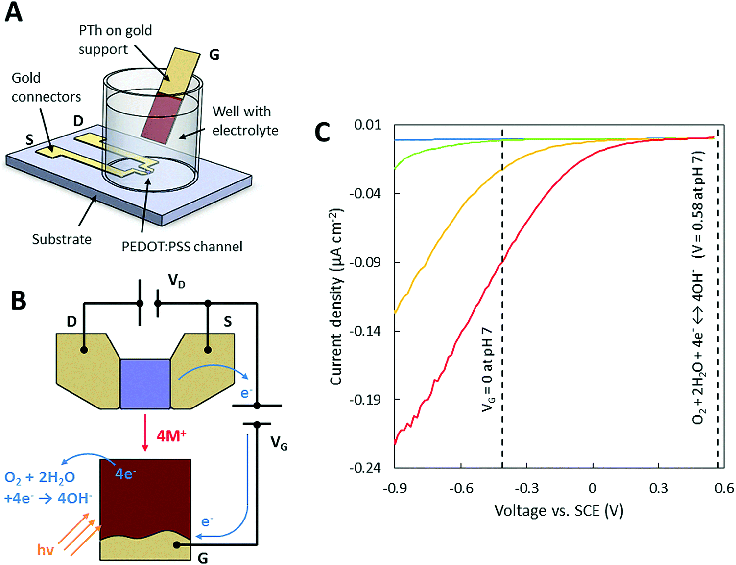 | ||
| Fig. 1 Schematics of the light-enhanced OECT (light sensor) used for measurements and its connection with the measuring device and preliminary material characterization. (A) Wiring layout of the transistor with the grey box indicating the electrolyte. (B) Schematic of the light-doping mechanism in the OECT setup. The distance between the light source and the electrode is 2 cm. The measurements performed in 0.1 M sodium chloride solution (pH 7). (C) Standard three-electrode measurements with an SCE as a reference and titanium mesh as a counter electrode. Linear voltage sweep (50 mV s−1) of polythiophene in the dark with nitrogen bubbling into the electrolyte (blue), in the dark with air bubbling into the electrolyte (green), under illumination (1820 W m−2) and with air bubbling into the electrolyte (yellow) and under illumination (2400 W m−2) and with air bubbling into the electrolyte (red). The measurements were performed in 0.1 M NaCl (pH 7). | ||
The presented sensor relies on three materials PEDOT:PSS, PTh and gold. PTh is the only material in this configuration that promotes an increase in current upon illumination in the presence of dissolved oxygen (Fig. S1, ESI†) at potentials relevant for the OECT operation. This is due to the oxygen reduction reaction4,15 (eqn (1)) and is dependent on the oxygen concentration and light irradiation (Fig. 1C). Gold was used as a conductive substrate for the poorly conductive polythiophene.
| O2 + 2H2O + 4e− ↔ 4OH− | (1) |
In a standard OECT, the application of an appropriate bias at the gate (gate voltage, VG) causes the ions from the electrolyte to enter the polymer channel and dope or de-dope it, thereby increasing or decreasing the drain current. The de-doping process in PEDOT:PSS is shown below (eqn (2)) where M represents a monovalent cation such as Na+.16–18
| n(PEDOT+:PSS−) + nM+ + ne− ↔ n(PEDOT0:PSS−:M+) | (2) |
The measurements performed with a ferrocene redox couple dissolved in an aqueous electrolyte showed that VG = 0 V in the OECT setup corresponding to roughly −0.46 V vs. SCE at a pH of 7 (Fig. 1C). Hence, current amplification due to the presence of light occurs for both positive and negative gate potentials (VG) up to 0.58 V vs. SCE. This potential limitation is guided by the electrochemistry of oxygen reduction and can be predicted using the Nernst equation. According to Fig. 1C, the current ratio between the dark state and upon illumination decreases at higher gate potentials (VG), which can be associated with a lower signal amplification when operating at higher gate potentials (Fig. S2A and B, ESI†).
The photo-induced oxygen reduction reaction can be used to sense and quantify light intensity. A two-electrode setup, where PTh on a gold support acts as the cathode and PEDOT:PSS as the anode material (both electrodes are 5 × 5 mm), showed that this simple setup can be used for light sensing by itself (Fig. 2B). However, the resulting current is in the range of nanoamps (green traces have been multiplied by 100 for comparison with the two other OECT traces). Using the same electrodes in an OECT setup showed an increase in current by a factor of more than 100 (Fig. 2B). In the presented case, both electrodes are of the same size. Hence, the OECT amplifies the small photocurrent produced by the gate electrode into an easily detectable drain current. The performance can be even further enhanced by having a large gate and a small channel.
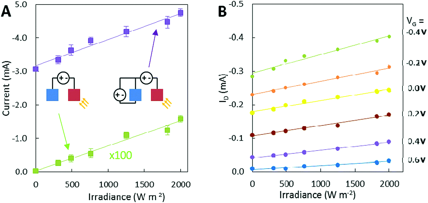 | ||
| Fig. 2 OECT light sensor. (A) Sensitivity measurements. Current response with respect to light intensity for the OECT when VD = −0.6 V and VG = 0 V (purple); a two-electrode setup with a −0.6 V bias between electrodes is also shown (green). The current values for the two-electrode measurements have been multiplied by 100 for comparison. The area of the electrodes was 5 × 5 mm. (B) The OECT current response to different light stimulation on the poly(bithiophene) gate. Drain voltage is −0.6 V, and the gate voltage steps from −0.4 to 0.6 V with a step of 0.2 V. Data derived from the I–V curves. | ||
In the OECT configuration with a PTh gate electrode, the illumination of PTh and the following oxygen reduction reaction forces an oxidation reaction to occur on the PEDOT:PSS channel, which in this situation plays the role of a counter electrode to the PTh. The oxidation of PEDOT:PSS results in a higher conductivity of the channel and thereby higher drain currents. The extraction of Na+ ions from the channel by the oxidation of PEDOT:PSS provides charge neutrality in the electrolyte (Fig. 1B) when OH− is produced at the gate (eqn (1)).
Organic light sensing is only one possible application for this novel device. Combining two or more OECTs allows the creation of opto-logic gates and optical circuits. OECTs have been employed to create logic devices and circuits before,19,20 and a recent study has shown the application of ion transistors in logic gates.21 Going one step further, we have created opto-logic gates (Fig. 3) which can be used as opto-electronic interfaces. The proposed circuits operate at very low voltages, making these devices excellent candidates for portable and low-power applications. As mentioned previously, operating the OECT at high transconductance regimes is favorable for sensor applications; however, for logic gate applications, the desired operation mode is at the highest current gain in order to get a significant on-/off-state current difference. The measurements were performed at VD = −0.6 V and VG = 0.6 V. The gate voltage was applied to preliminarily de-dope the channel material and to get very low drain currents – a logic state of “0”. At VG = 0.6 V upon irradiance of 1820 W m−2, the ID values increase more than twice (Fig. 3A) – a logic state of “1”. Two light-sensitive OECTs have been connected in series (AND gate) and in parallel (OR gate) (Fig. 3A and B). Light from two similar light sources was emitted directly on the devices, making sure that light from one device does not interfere with the other device. These simple circuits have proven to be potential candidates for an opto-electronic interface, where light is converted into an electronic logic value. To our knowledge, this is the very first report of such an interface based on organic materials and operating at very low-voltage regimes.
 | ||
| Fig. 3 Opto-logic gates. (A and B) Schematics and logic tables and circuits used for opto-logic gates, AND gates and OR gates respectively. (C) The AND gate response depending on the optical input signal. (D) The OR gate response depending on the optical input signal. The measurements were performed in 0.1 M NaCl electrolyte, and the ON-state was simulated with 1820 W m−2 irradiance from a Leica KL 2500 LCD lamp. VD = −0.6 V and VG = 0.5 V (AND) and VG = 0.6 V (OR). The logic threshold was −0.07 mA. Further explanation, working principles and mathematical equations for opto-logic gates can be found in the ESI† (Fig. S3, ESI† and the corresponding text). | ||
In order to compare both opto-logic gates, different gate voltages have been applied to achieve similar drain current values. The logic threshold was −0.07 mA.
The implementation of the light-sensitive conjugated polymer, polythiophene, into the OECT platform has been successful and thus light-responsive OECT devices have been demonstrated. We have shown an organic light sensor that is cheap and relatively easy to manufacture. The device operates at very low voltages (around 0.6 V) and shows a high transconductance at low gate potentials (0.38 mS at 0.06 V) as well as high and linear light sensitivity. An additional advantage of the presented device is its very fast response (couple of seconds) to light. Using the OECT for light sensing allows for the miniaturization and scalability of the device. Furthermore, it has been demonstrated that it is possible to manufacture arrays of these devices and thereby they have the potential to be used in opto-logic applications, where optical signals are converted to electrical signals.
The transient response of the transistor was estimated to be around 11 seconds when increasing the gate voltage and about 16–17 seconds when decreasing the applied voltage. Similarly, the response time to increased irradiation was 8 seconds on average, while the transient response to decreased irradiation was much longer and took 38 seconds on average.
Here, two transistors are connected either in series (AND gate) or parallel (OR gate) and act as a low-voltage organic opto-electronic transducer. A large part of the current technology relies on electronics and electrical signals, and the optical signals in many cases have to be converted into electrical signals for further processing. The developed device acts as such an interface. Further optimization of the sensor's architecture can lead to improved performance. The monolithic integration of the device through lithography can result in further scalability and integration of transistor arrays for use in applications where an opto-electrical interface is essential.
Experimental section
Device fabrication
The fabrication process was similar to that reported previously22,23 including the deposition and patterning of gold, parylene, and PEDOT:PSS. Source/drain contacts were patterned by a lift-off process, using an S1813 photoresist, exposed to UV light through a SUSS MBJ4 contact aligner, and developed using an MF-26 developer. 5 nm of chromium and 100 nm of gold were subsequently deposited using a metal evaporator, and metal lift-off was carried out in acetone. Metal interconnects and pads were insulated by depositing 2 μm of parylene C using an SCS Labcoater 2, using a silane adhesion promoter. A dilute solution of industrial cleaner (Micro-90) was subsequently spin coated (to act as an anti-adhesive) for a second, sacrificial 2 μm parylene – C film. The samples were subsequently patterned with a 5 μm thick layer of an AZ9260 photoresist and an AZ developer (AZ Electronic Materials). The patterned areas were opened by reactive ion etching with oxygen plasma using an Oxford Plasmalab 80 Plus. PEDOT:PSS + 1 wt% GOPS in solution was spin coated at 3000 rpm, and baked for 90 s at 100 °C. The second layer of parylene was peeled off with a subsequent rinsing in DI water and baking at 140 °C for 30 min.Polymer precursor 2,2′-bithiophene (BTh) was obtained from Sigma-Aldrich. Ferric p-toluenesulfonate (Fe(III)PTS) in 40% butanol was supplied by YACOO Chemical Reagent Co. Ltd. All materials were used without further purification. Oxidant solution was cast onto the substrate and spin-coated using a Laurell spin-coater at 1500 rpm for 30 s in order to obtain a uniform thickness. Polymerization took place in a closed chamber at atmospheric pressure and a controlled temperature of 70 °C for 1 h, where the substrate coated with the oxidant was exposed to monomer vapor. Once the polymerization was done, the films were left to cool down to room temperature, rinsed with ethanol, and kept in ethanol for around 12 h to remove excess oxidant and residual reduction products and other impurities formed during the polymerization process. The whole procedure is described elsewhere.23,24 A polybithiophene gate electrode was deposited on gold sputtered Mylar (around 15 Ω sqr−1). The gold layer was used as a conductivity support for the poorly conductive polythiophene.
Electrochemical measurements – linear voltage sweep and chronoamperometry
Material characterization was performed on a Bio-logic VMP3 potentiostat in a normal three-electrode electrochemical setup, where the distances between the electrodes were kept constant. A titanium mesh and a saturated calomel electrode (SCE) were used as the counter and reference electrodes, respectively. The measurements were performed in an aqueous solution of 0.1 M NaCl (pH 7.1). A linear voltage sweep was then carried out by continuously bubbling air or nitrogen through the electrolyte. All tests were performed both under illumination from an external light source and in the dark. A Leica KL 2500 LCD was used as the light source. The measurements were performed at a scan rate of 50 mV s−1.Chronoamperometry tests were performed under the same conditions as for the linear voltage sweep. A constant potential of −0.4 V was applied between the electrodes. Chronoamperometry measurements were run for a total of 15 min, of which the first 5 minutes were performed in the dark, following 15 min under illumination of 2400 W m−2 with the last 5 min again in the dark. Air was continuously bubbled through the electrolyte. The distance between the light source and the electrode was 2 cm.
To identify voltage relations between the three-electrode setup and the OECT, the ferrocene redox couple was dissolved in an aqueous electrolyte and the redox peaks were measured in a three-electrode setup and an OECT setup. The position of the reduction and oxidation peaks of ferrocene was then identified to find out that VG = 0 V in the OECT corresponds to −0.46 V vs. SCE at a pH of 7.
OECT light sensor characterization
Sensor characterization was performed in an aqueous electrolyte (pH 7.1) of 0.1 M sodium chloride (NaCl). Transistor characteristics were measured using a Keithley 2612A Sourcemeter and customized LabVIEW software. The I–V characteristics were investigated by sweeping the source–drain voltage and measuring the corresponding current. Voltage was swept from 0 to −0.6 V with a voltage step of 0.01 V. This procedure has been repeated for different gate electrode voltages, starting from 0 V and moving up to 0.6 V with a voltage step of 0.1 V. The I–V measurements were performed in the dark and upon light illumination on the gate electrode. Light irradiance used in this measurement was around 1820 W m−2, which was produced using a Leica KL 1500 LCD.The time characteristic measurement was also carried out using a Keithley 2612A SourceMeter, the drain–source voltage was kept at −0.6 V, at different gate potentials ranging from −0.4 up to 0.6 V, with a step of 0.2 V. The source–drain current (ID) was measured in the dark, as well as at different irradiance levels, starting from 310, 490, 760, 1250, 1820 and 2000 W m−2.
The transfer curve and its associated transconductance were derived from the I–V curves at VD = −0.6 V. The distance between the light source and the electrode was 2 cm.
Opto-logic gate characterization
OECTs have been connected in series (AND gate) or in parallel (OR gate) (Fig. 3A and B). Gate characterization was performed using an aqueous electrolyte (pH 7.1) of 0.1 M sodium chloride (NaCl). The time characteristic measurement (opto-logic response) was carried out using a Keithley 2612A SourceMeter. The drain–source voltage was kept at −0.6 V at a fixed gate potential of 0.6 V. The source–drain current (ID) was measured in the dark (closed), as well as at 2000 W m−2 irradiance (open). The light source used in this measurement was produced using a Leica KL 2500 LCD.Conflicts of interest
There are no conflicts to declare.References
- J. Janata and M. Josowicz, Nat. Mater., 2003, 2, 19 CrossRef CAS PubMed.
- A. Facchetti, Nat. Mater., 2013, 12, 598 CrossRef CAS PubMed.
- J. R. Tumbleston, B. A. Collins, L. Yang, A. C. Stuart, E. Gann, W. Ma, W. You and H. Ade, Nat. Photonics, 2014, 8, 385 CrossRef CAS.
- B. Kolodziejczyk, O. Winther-Jensen, D. R. MacFarlane and B. Winther-Jensen, J. Mater. Chem., 2012, 22, 10821 RSC.
- C. H. Ng, O. Winther-Jensen, B. Kolodziejczyk, C. A. Ohlin and B. Winther-Jensen, Int. J. Hydrogen Energy, 2014, 39, 18230 CrossRef CAS.
- C. H. Ng, O. Winther-Jensen, C. A. Ohlina and B. Winther-Jensen, Int. J. Hydrogen Energy, 2017, 42, 886 CrossRef CAS.
- D. Ghezzi, M. R. Antognazza, M. Dal Maschio, E. Lanzarini, F. Benfenati and G. Lanzani, Nat. Commun., 2011, 2, 166 CrossRef PubMed.
- P. H. Prevot, D. Alvares, A. Micolich, N. Lovell and F. Ladouceur, J. Org. Semicond., 2015, 3, 8 CrossRef CAS.
- R. Ahmed, A. Kadashchuk, C. Simbrunner, G. Schwabegger, M. Havlicek, E. Glowacki, N. S. Sariciftci, M. A. Baig and H. Sitter, Org. Electron., 2014, 15, 175 CrossRef CAS.
- K. E. Lee, J. U. Lee, D. G. Seong, M.-K. Um and W. Lee, J. Phys. Chem. C, 2016, 120(40), 23172–23179 CAS.
- H. Bink, Y. Lai, S. R. Saudari, B. Helfer, J. Viventi, J. Van der Spiegel, B. Litt and C. Kagan, Conf. Proc. IEEE Eng. Med. Biol. Soc., 2011, 5400–5403 Search PubMed.
- X. Strakosas, M. Bongo and R. M. Owens, J. Appl. Polym. Sci., 2015, 132, 41735 CrossRef.
- I. Gualandi, M. Marzocchi, A. Achilli, D. Cavedale, A. Bonfiglio and B. Fraboni, Sci. Rep., 2016, 6, 33637 CrossRef CAS PubMed.
- M. Hausser, Nat. Methods, 2014, 11, 1012 CrossRef CAS PubMed.
- B. Winther-Jensen, O. Winther-Jensen, M. Forsyth and D. R. MacFarlane, Science, 2008, 321, 671 CrossRef CAS PubMed.
- P. Andersson Ersman, D. Nilsson, J. Kawahara, G. Gustafsson and M. Berggren, Org. Electron., 2013, 14, 1276 CrossRef CAS.
- D. Nilsson, M. Chen, T. Kugler, T. Remonen, M. Armgarth and M. Berggren, Adv. Mater., 2002, 14, 51 CrossRef CAS.
- D. Nilsson, N. Robinson, M. Berggren and R. Forchheimer, Adv. Mater., 2005, 17, 353 CrossRef CAS.
- D. De Rossi, Nat. Mater., 2007, 6, 328 CrossRef CAS PubMed.
- K. Tybrandt, R. Forchheimer and M. Berggren, Nat. Commun., 2012, 3, 871 CrossRef PubMed.
- D. Khodagholy, J. Rivnay, M. Sessolo, M. Gurfinkel, P. Leleux, L. H. Jimison, E. Stavrinidou, T. Herve, S. Sanaur, R. M. Owens and G. G. Malliaras, Nat. Commun., 2013, 4 Search PubMed.
- X. Strakosas, M. Sessolo, A. Hama, J. Rivnay, E. Stavrinidou, G. G. Malliaras and R. M. Owens, J. Mater. Chem. B, 2014, 2, 2537 RSC.
- B. Kolodziejczyk, D. Mayevsky and B. Winther-Jensen, RSC Adv., 2013, 3, 4568 RSC.
- P. M. Bayley, B. Winther-Jensen, D. R. MacFarlane, N. M. Rocher and M. Forsyth, React. Funct. Polym., 2008, 68, 1119 CrossRef CAS.
Footnote |
| † Electronic supplementary information (ESI) available. See DOI: 10.1039/c7mh00818j |
| This journal is © The Royal Society of Chemistry 2018 |