
Determination of the maximum thickness for directed self-assembly of cylinder-forming PS-b-PMMA films on chemical patterns
Yadong
Liu
and
Shengxiang
Ji
 *
*
Key Laboratory of Polymer Ecomaterials, Changchun Institute of Applied Chemistry, Chinese Academy of Sciences, 5625 Renmin Street, Changchun 130022, China. E-mail: sji@ciac.ac.cn
First published on 5th December 2017
Abstract
Previous studies on directed self-assembly (DSA) of cylinder-forming PS-b-PMMA mainly use films with a thickness comparable to the natural period of the block copolymer, Lo. It is unclear how thick the cylinder-forming PS-b-PMMA film can be directed to assemble on chemical patterns. In this work, a feasible approach is developed to determine the maximum thickness for DSA of cylinder-forming PS-b-PMMA films. The chemical pattern with a controlled correlation length (ξ) is fabricated by molecular transfer printing (MTP) by replicating the surface domain pattern of the template blend film and used to direct the self-assembly of the same blend film. The transition from substrate-controlled DSA to surface-controlled self-assembly is located in assembled films on MTP replica patterns with the thickness between 4.9Lo and 5.7Lo by comparing the ξ of the assembled film with the ξ of the original template. DSA of cylinder-forming PS-b-PMMA is achieved in films with thickness up to at least 4.9Lo. When the film is thicker than 5.7Lo, the substrate and surface effects decouple and the free surface controls the film surface morphology.
Design, System, ApplicationBlock copolymer lithography is emerging as one of the leading technologies to pattern well-defined dense features at the scale of 10 nm and below. For pattern transfer applications, it is necessary to have a perpendicular orientation of block copolymer domains and a thick film is beneficial because of the low etching selectivity between block copolymers and the substrate. We present a feasible method to determine the maximum thickness for directed self-assembly of cylinder-forming PS-b-PMMA films on chemical patterns. The transition from substrate-controlled directed self-assembly to surface-controlled self-assembly is located in assembled films on chemical patterns, and directed self-assembly of cylinder-forming PS-b-PMMA films is achieved in films with a thickness of up to ∼5Lo. The fundamental impact of the present work is that this method might be extended to other block copolymer systems for determination of the thickness range for directed self-assembly. |
Introduction
Directed self-assembly (DSA) of block copolymer (BCP) films has been successfully demonstrated on chemical patterns with a variety of pattern geometries,1 including arrays of lines,2–11 bends,4,8 jogs,12,13 T-junctions,12 hexagonal spots,14,15 square and rectangular spots,16,17 concentric circles,18 checkerboards,19 rectangular patterns7 and isolated structures,12 with a high degree of perfection and registration. For pattern transfer applications, it is necessary to have a perpendicular orientation of either cylindrical or lamellar BCP domains through the film thickness and a thick film is beneficial because of the relatively low etching selectivity between organic polymers and the underlying silicon substrate. In thin films, BCPs nucleate from both interfaces and the competition between the BCP/air interaction and the BCP/substrate interaction determines the orientation of the BCP domains. As the film becomes thicker and thicker, the substrate effect gradually dissipates and the BCP/air interaction will be dominant at the surface.20 It is critical to determine the thickness range for the assembly of perpendicular domains in films, especially for the purpose of pattern transfer application.Poly(styrene-b-methyl methacrylate) (PS-b-PMMA) is the benchmark material for DSA studies since the surface energies (γ) of PS and PMMA are nearly equal in a large temperature range21 and perpendicular domains can be easily obtained near the film surface. DSA studies on lamellae-forming PS-b-PMMA mostly use films with the film thickness (Lz) comparable to the natural period of the BCP (Lo).2–11 Welander et al. determined the thickness range for the perpendicular orientation of lamellae-forming PS-b-PMMA on striped chemical patterns by cross-sectional SEM analysis. They found that DSA of lamellae-forming PS-b-PMMA was achieved in films with Lz up to ∼10Lo when the pattern period (Ls) matches Lo.22
The thickness range for DSA of cylinder-forming PS-b-PMMA is unclear. Previous studies on DSA of cylinder-forming PS-b-PMMA focus on films with Lz ≈ Lo.14,15,23–27 There are a number of studies on self-assembly of relatively thick cylinder-forming PS-b-PMMA films on homogeneous substrates. Han et al. claimed that the perpendicularly oriented cylinders were up to 900 nm in films on neutral surfaces.28 Ryu et al. reported that when the composition of random copolymer brushes was close to the optimal neutral composition, the thickness range to achieve perpendicular cylinders was largest.29 Ji et al. observed a transition from substrate-dominant to surface-dominant assembly behaviors in cylinder-forming PS-b-PMMA films on both neutral and preferential substrates by SEM analysis.20 The transition thickness is between ∼3Lo (95 nm) and ∼6Lo (189 nm). At Lz > 6Lo, the surface morphologies are independent of the substrate chemistry and the cylindrical domains are perpendicular to the film near the surface at 230 °C, but do not propagate through the entire film. Lupi et al. probed the thickness range for the perpendicular orientation of the cylinder-forming PS-b-PMMA film by a lift-off process and found that perpendicular cylinders could be obtained in films with Lz up to 170 nm.30 In a following study by Lupi et al., they then used GISAXS to characterize the film morphologies and observed the transition from perpendicular cylinders to a mixed orientation of cylinders at a thickness of ∼160 nm in cylinder-forming PS-b-PMMA films.31 At Lz > 160 nm, the effects of the free surface and substrate on the film morphology decoupled.
In this work, we systematically studied the self-assembly behaviors of cylinder-forming PS-b-PMMA films with different Lzs to determine the maximum thickness for DSA on chemical patterns. We fabricated chemical patterns of hexagonal arrays of spots with a controlled correlation length (ξ) by molecular transfer printing (MTP)32 (Fig. 1) from thick films of PS-b-PMMA/PS–OH/PMMA–OH ternary blend instead of electron beam lithography (EBL) or extreme ultra-violet interference lithography (EUV-IL). We assembled the same blend films with various Lzs at different temperatures on MTP substrates, quantified the ξs, and compared the ξs of hexagons in the assembled films on the MTP replica and in the original template to locate the transition thickness. The rationale is that the surface morphology will be exactly the same as the pattern geometry under DSA conditions and the ξ of the assembled film on the replica will be the same as the ξ of the corresponding template. The two ξs will be significantly different when the film is thicker than a threshold thickness above which the free surface effect will dominate. The success of this method relies on two prerequisites: 1) MTP can faithfully replicate the surface structure and 2) DSA has extremely high fidelity.
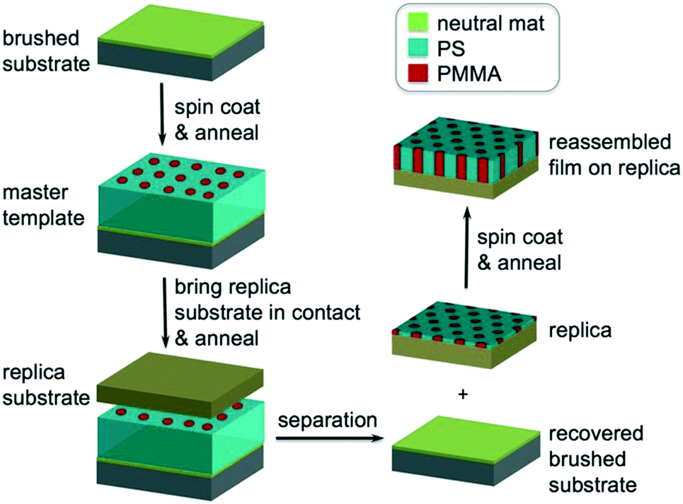 | ||
| Fig. 1 The process of molecular transfer printing (MTP). A ternary blend film of PS-b-PMMA, PS–OH and PMMA–OH is deposited on the brushed substrate and thermally annealed to form the master template. A replica substrate is then brought into contact with the master film. The sandwiched structure is thermally annealed and then separated by solvent washing to generate a replica and recover the brushed substrate. The same blend film is directed to assemble on the replica. | ||
Experimental
Materials
PS-b-PMMA (Mn = 46–21 kg mol−1, Lo = 31.5 nm, PDI = 1.06) was purchased from Polymer Source, Inc. Hydroxyl-terminated polystyrene (PS–OH, Mn = 6 kg mol−1, PDI = 1.12) and hydroxyl-terminated poly(methyl methacrylate) (PMMA–OH, Mn = 6 kg mol−1, PDI = 1.16) were synthesized by atomic transfer radical polymerization (ATRP) using 2-hydroxyethyl-2-bromoisobutyrate as the initiator.33 Crosslinkable poly(styrene-ran-methyl methacrylate-ran-glycidal methacrylate) (P(S-r-MMA-r-GMA), Mn = 30 kg mol−1, PDI = 1.7) with 63 mol% of styrene and 4 mol% GMA fractions were synthesized by free radical polymerization.6Preparation of the master template
A 0.2 wt% toluene solution of P(S-r-MMA-r-GMA) was spin-coated onto the piranha-cleaned silicon substrate, and the deposited film (∼6 nm) was thermally annealed at 190 °C for 12 h.6 The uncrosslinked brush polymers were removed by sonication in toluene 5 times to yield a crosslinked mat of ∼6 nm thickness.Solutions of a ternary blend of 92 wt% PS-b-PMMA, 5 wt% PS–OH and 3 wt% PMMA–OH in toluene were spin-coated on the crosslinked mat to yield films with Lz ranging from 200–400 nm. The blend films were then annealed at 230 °C for various times to form template films.
Fabrication of replica chemical patterns by molecular transfer printing (MTP)
The MTP process was developed by Ji et al.32 A silicon substrate (replica substrate) was cleaned by piranha treatment and then placed on the surface of the assembled template film (master template). The sandwiched structure was clamped using two-parallel clamps, annealed at 160 °C for 24 h under vacuum, and separated with toluene to generate a replica chemical pattern of alternating regions of grafted PS and PMMA homopolymer brushes.Directed self-assembly of blends on chemical patterns
Solutions of the ternary blend of 92 wt% PS-b-PMMA, 5 wt% PS–OH and 3 wt% PMMA–OH in toluene were spin-coated on the replicas to yield films with Lz ranging from 30–340 nm. The blend films were then annealed at 190 and 230 °C for various times under vacuum.Calculation of the correlation length (ξ)
The film surface morphologies were characterized by a Zeiss Merlin FE-SEM with 1 kV accelerating voltage. The size of each image was 4.3 μm × 5.7 μm. The images were processed using a Matlab® program which performed four operations on each image: image binarization, domain centroid localization, defect exclusion, and calculation of the auto correlation function (ACF).34 The ξ of the perpendicular cylinders was calculated by fitting the ACF to an exponential function, ACF = exp(−r/ξ), where r is the distance from the center domain in the ACF analysis. Five SEM images were taken from different areas on each sample and the ξ of each sample was averaged from five images.Results and discussion
Preparation of MTP templates
In block copolymer lithography, the substrate is usually modified by brushes to control the domain orientation of BCPs.35–39 The MTP master templates were prepared by spin-coating solutions of the ternary blend of PS-b-PMMA, PS–OH and PMMA–OH on neutral mats, and annealing the resulting films at 230 °C for 1.5 hours (Fig. 1). Low molecular weight PS–OH and PMMA–OH were used as inks and confined within their respective PS and PMMA domains. Compared to PS-b-PMMA, addition of low molecular weight PS–OH and PMMA–OH did not change the period, and the blend period (LB) was the same as the Lo of PS-b-PMMA by SAXS analysis. Three different film thicknesses (Lz = 205, 300, and 390 nm) were chosen for investigation. At 230 °C, the surface energies (γ) of PS and PMMA are nearly equal, leading to the formation of hexagonal arrays of perpendicular cylinders at film surfaces. Ji et al. reported that hexagonal arrays of perpendicular cylinders could be obtained on the PS-b-PMMA (Mn = 46–21 kg mol−1) film surface at 230 °C regardless of the substrate chemistry when Lz was thicker than 5.68Lo.20 A representative SEM image of the surface morphology of the master template film is shown in Fig. 2. In the corresponding Voronoi plot, pentagons (blue) and heptagons (red) are identified as defects and conjugated defects form the grain boundary. These grains have different grain orientations and sizes. Some grains could be as large as several μm2 in thick films.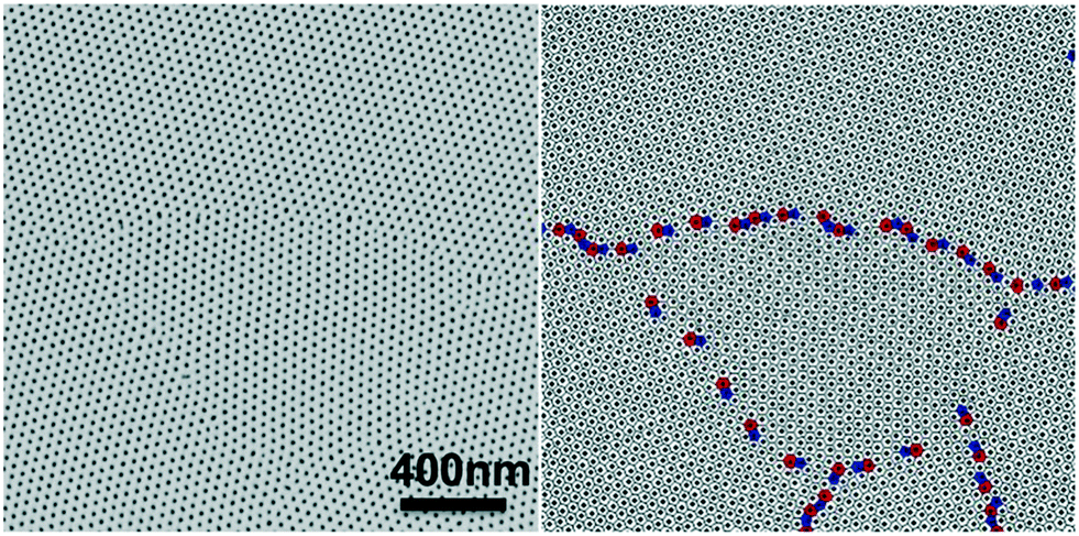 | ||
| Fig. 2 Representative SEM image of the 205 nm-thick blend film annealed at 230 °C for 1.5 hours on the neutral mat and its corresponding Voronoi plot. | ||
The ξs of hexagonal arrays of perpendicular cylinders were calculated and summarized in Table 1. The ξs are 390 ± 46 nm, 465 ± 40 nm, and 542 ± 85 nm for films with Lz = 205, 300, and 390 nm, respectively. The ξ scales with the annealing time according to a power law in thick films.20 A shorter annealing time led to smaller ξs, but the Voronoi plot of the SEM image showed that it had a portion of discrete pentagon–heptagon pairs within the grains. A longer annealing time could effectively eliminate the defects to form larger grains. The resolution limit of SEM imaging leads to our choice of films with ξs of ∼400–600 nm to guarantee enough representative grains in one SEM image.
| ξ of template films on neutral mats | ξ of assembled films on corresponding replicas | |||
|---|---|---|---|---|
| L z (nm) | 230 °C | L z (nm) | 190 °C | 230 °C |
| 205 | 390 ± 46 | 30 | 378 ± 35 | 382 ± 55 |
| 300 | 465 ± 40 | 30 | 460 ± 50 | 472 ± 48 |
| 390 | 542 ± 85 | 30 | 555 ± 72 | 560 ± 81 |
Quantification of the fidelity of the MTP process
MTP has been demonstrated to replicate the surface domain pattern of BCP films with high degrees of perfection and fidelity for regular and non-regular patterns.17,20,32,40–46 We fabricated chemical patterns of hexagonal arrays of spots with controlled ξs by MTP instead of writing patterns with an infinite ξ by EBL or EUV-IL. In the MTP process, PS–OH and PMMA–OH inks were confined within their respective PS and PMMA domains in PS-b-PMMA BCPs, and reacted with the native oxide layer on the replica substrate to replicate the surface domain pattern of the master film to create a pattern of spot arrays of grafted PMMA homopolymers surrounded by grafted PS homopolymers.The high fidelity of the MTP process will allow the replica pattern to have the same ξ as the master template film. For each template, the corresponding replica was cut into two pieces which were then used to direct the assembly of 30 nm-thick films of the same blend at 190 °C and 230 °C for 3 hours, respectively. The surface structures were imaged by SEM and perpendicularly oriented hexagonal arrays of cylinders were obtained on the film surface in all films. For each sample, five images were taken from different areas. The ξs of the assembled films were calculated and averaged from the five SEM images (Table 1). For replica patterns from the same template, ξs were almost the same for the two films assembled at different temperatures, 190 °C and 230 °C, and were close to the ξ of the corresponding master template, demonstrating the high fidelity of the MTP process. In comparison, the ξs of the same 30 nm-thick blend films that were annealed at 190 °C and 230 °C for 3 hours on neutral mats were ∼210 nm and 280 nm, respectively, much lower than the ξs of films assembled on MTP replicas.
Temperature- and thickness-dependent DSA of ternary blends on MTP replicas
The blend film with ξ = 465 ± 40 nm was chosen as the master template for MTP. After MTP, the replica had the same ξ as the template and was used to direct the assembly of the ternary blend films with Lz = 30–340 nm at 190 °C for 24 hours and 230 °C for 3 hours, respectively. For films that were annealed at 230 °C, hexagonal arrays of perpendicular cylinders were obtained in films with the thickness ranging from 30–340 nm. It is difficult to determine the transition thickness for films annealed at 230 °C by SEM analysis. Fig. 3A shows a representative SEM image of a 180 nm-thick blend film that was directed to assemble on the replica at 230 °C. When the films were annealed at 190 °C, thickness-dependent assembly behaviors were observed in the blend films on replicas. At Lz ≤ 155 nm or 4.9Lo, hexagonal arrays of perpendicular cylinders were obtained at the film surface; however, when Lz was increased to 180 nm (5.7Lo), hexagonal arrays of perpendicular cylinders along with a small fraction of parallel cylinders were observed on the film surface (Fig. 3B). In comparison, when the blend films were assembled on silicon substrates at 190 °C, a transition from parallel cylinders to perpendicular cylinders with coexisting parallel cylinders occurred around 4Lo, but defect-free assembly of perpendicular cylinders was not observed even in thicker films.20 The different assembly behaviors of the blend films on the MTP replicas and silicon-substrates are attributed to the competition between the substrate and the free surface. | ||
| Fig. 3 SEM images of 180 nm-thick blend films that were directed to assemble on MTP replicas at A) 230 °C and B) 190 °C, respectively, for 3 hours. Defects of parallel cylinders are present at the film surface in B). | ||
Analysis of the thickness-dependent ξs in assembled films is a quantitative approach to determine the transition thickness. The ξs of assembled films on MTP replicas were calculated and plotted in Fig. 4. The ξs remained constant and were the same as the ξ of the original template when Lz ≤ 155 nm or 4.9Lo at 230 °C. When Lz ≥ 180 nm or 5.7Lo, the ξ monotonically increased with Lz. The same blend films with Lz = 50–285 nm were annealed at 230 °C for 3 hours on neutral mats, and their ξs were calculated and also plotted in Fig. 4. The ξs linearly increased with Lz in the thickness range on neutral mats20 and were close to the ξs of films assembled on replicas at Lz ≥ 180 nm or 5.7Lo. These results indicated that the effects of the free surface and substrate decoupled at Lz ≥ 5.7Lo and the surface morphologies were not controlled by the underlying substrates. Although perpendicular cylinders were obtained at the free surface in thick films at 230 °C, the perpendicular cylinders nucleated at the substrate interface and the free surface merged at a certain thickness and might not connect with each other, leading to the deviation of the ξs of films on replicas from that of the template.
 | ||
| Fig. 4 ξs of blend films assembled on MTP replicas (ξ = 465 ± 40 nm) at 230 °C for 3 hours (green square) and 190 °C for 24 hours (orange dot) and blend films annealed at 230 °C for 3 hours (open red square) and 190 °C for 24 hours (open blue circle) on neutral mats. | ||
The blend films also had thickness-dependent ξs when they were directed to assemble on replicas at 190 °C. The ξs also remained constant and were the same as the ξs of the original template at Lz ≤ 155 nm or 4.9Lo, but the ξ dropped to ∼210 nm at Lz ≥ 180 nm or 5.7Lo. The sharp drop in ξ was caused by the formation of defects of parallel cylinders at the film surface because of the slight difference in γ at 190 °C. In comparison, when the blend films were annealed on neutral mats at 190 °C, the ξs were almost the same (∼250 nm) and did not increase with Lz.20 The formation of defects of parallel cylinders at 190 °C is a simple criterion to determine the maximum thickness for DSA.
The film morphology does not change with the annealing time if the film is directed to assemble on chemical patterns, and Lz is smaller than the transition thickness. The effect of the annealing time on the evolution of ξs was studied in films assembled on replicas with two different Lzs. Two sets of films on replicas with Lz = 128 nm (∼4Lo) and 190 nm (∼6Lo) that were outside of the transition thickness range, 4.9Lo–5.7Lo, were annealed at 230 °C for 3–24 hours. The ξs of these films were calculated and plotted in Fig. 5. The ξs of films with Lz = 184 nm increased with the annealing time and were larger than the ξ of the original template, also proving that the surface morphology was no longer controlled by the substrate. In contrast, when Lz = 125 nm, which was smaller than 155 nm, the ξs were the same as the ξ of the original template and remained constant even with the increase of the annealing time, which is a characteristic behavior of DSA.
 | ||
| Fig. 5 ξs of blend films on MTP replicas that were annealed at 230 °C for 3–24 hours with Lzs of 128 nm and 190 nm. | ||
Determination of the thickness range for the perpendicular orientation of BCP domains is a useful probe to characterize the strength of the substrate effect on self-assembly of a BCP film. Previously, Ji et al. observed that the substrate effect was dominant in films with Lz ≲ 4Lo in cylinder-forming PS-b-PMMA films at 190–230 °C on both silicon substrates and neutral brushes.20 Lupi et al. studied the same cylinder-forming PS-b-PMMA on neutral brushes and showed that the perpendicular orientation of domains was obtained in films with an Lz of up to 170 nm by a lift-off process at 270 °C.30 We also used the same cylinder-forming PS-b-PMMA for DSA and the maximal thickness for DSA on chemical patterns was determined to be between 155–180 nm (4.9–5.7Lo) which agreed well with Lupi et al.'s result. These observations suggest that the strength of the substrate effect on BCP self-assembly may not be dependent on the substrate chemistry, but the substrate modification determines the orientation and placement of domains near the substrates. Since the surface energies of PS and PMMA are nearly equal under DSA conditions, a perpendicular orientation of domains is obtained through the entire film at Lz < the transition thickness. For BCPs that do not have nearly equal surface energies, the BCP itself determines the thickness that perpendicular domains can be obtained in the film on either neutral brushes or chemical patterns.47
Conclusions
In summary, a facile method has been developed to characterize the maximum film thickness for DSA of cylinder-forming PS-b-PMMA. A strict criterion to locate the transition thickness range for substrate-controlled DSA to surface controlled self-assembly is to compare the ξs of cylinder-forming PS-b-PMMA films on replica chemical patterns with the ξ of the original template. The same transition thickness range is obtained for films that are directed to assemble on replicas at both 190 °C and 230 °C, and the maximum thickness for the DSA of cylinder-forming PS-b-PMMA films is between 155–180 nm (4.9–5.7Lo). Compared to cross-sectional TEM28 or SEM20,22 analysis and GISAXS analysis,48 characterization of the ξs of films uses more representative information and has advantages over the above methods in terms of sample preparation and defect detection. Moreover, the observation of the evolution of perpendicular cylinders to perpendicular cylinders with parallel defects at surface structures is an easy method to determine the transition thickness at 190 °C. This method might be extended to PS-b-PMMA with different volume fractions and even other block copolymer systems for the determination of the maximum film thickness for DSA.Conflicts of interest
There are no conflicts to declare.Acknowledgements
This work was financially supported by the National Natural Science Foundation of China (No. 51173181, 51373166), the “The Hundred Talents Program” from Chinese Academy of Sciences and the Department of Science and Technology of Jilin Province (No. 20160414032GH and 20150204027GX).Notes and references
- S. X. Ji, L. Wan, C. C. Liu and P. F. Nealey, Prog. Polym. Sci., 2016, 54–55, 76–127 CrossRef
.
- S. O. Kim, H. H. Solak, M. P. Stoykovich, N. J. Ferrier, J. J. de Pablo and P. F. Nealey, Nature, 2003, 424, 411–414 CrossRef CAS PubMed
- E. W. Edwards, M. F. Montague, H. H. Solak, C. J. Hawker and P. F. Nealey, Adv. Mater., 2004, 16, 1315–1319 CrossRef CAS
- M. P. Stoykovich, M. Muller, S. O. Kim, H. H. Solak, E. W. Edwards, J. J. de Pablo and P. F. Nealey, Science, 2005, 308, 1442–1446 CrossRef CAS PubMed
- J. Y. Cheng, C. T. Rettner, D. P. Sanders, H. C. Kim and W. D. Hinsberg, Adv. Mater., 2008, 20, 3155–3158 CrossRef CAS
- C. C. Liu, E. Han, M. S. Onses, C. J. Thode, S. X. Ji, P. Gopalan and P. F. Nealey, Macromolecules, 2011, 44, 1876–1885 CrossRef CAS
- R. Ruiz, E. Dobisz and T. R. Albrecht, ACS Nano, 2011, 5, 79–84 CrossRef CAS PubMed
- S. X. Ji, U. Nagpal, G. L. Liu, S. P. Delcambre, M. Muller, J. J. de Pablo and P. F. Nealey, ACS Nano, 2012, 6, 5440–5448 CrossRef CAS PubMed
- L. Wan, R. Ruiz, H. Gao, K. C. Patel and T. R. Albrecht, ACS Nano, 2015, 9, 7506–7514 CrossRef CAS PubMed
- X. Li, Y. D. Liu, L. Wan, Z. L. Li, H. Suh, J. X. Ren, L. E. Ocola, W. B. Hu, S. X. Ji and P. F. Nealey, ACS Macro Lett., 2016, 5, 396–401 CrossRef CAS
- Y. Y. Pang, L. Wan, G. C. Huang, X. S. Zhang, X. S. Jin, P. Xu, Y. D. Liu, M. M. Han, G. P. Wu and S. X. Ji, Macromolecules, 2017, 50, 6733–6741 CrossRef CAS
- M. P. Stoykovich, H. Kang, K. C. Daoulas, G. Liu, C. C. Liu, J. J. de Pablo, M. Mueller and P. F. Nealey, ACS Nano, 2007, 1, 168–175 CrossRef CAS PubMed
- G. L. Liu, C. S. Thomas, G. S. W. Craig and P. F. Nealey, Adv. Funct. Mater., 2010, 20, 1251–1257 CrossRef CAS
- S. M. Park, G. S. W. Craig, C. C. Liu, Y. H. La, N. J. Ferrier and P. F. Nealey, Macromolecules, 2008, 41, 9118–9123 CrossRef CAS
- R. Ruiz, H. M. Kang, F. A. Detcheverry, E. Dobisz, D. S. Kercher, T. R. Albrecht, J. J. de Pablo and P. F. Nealey, Science, 2008, 321, 936–939 CrossRef CAS PubMed
- S. M. Park, G. S. W. Craig, Y. H. La, H. H. Solak and P. F. Nealey, Macromolecules, 2007, 40, 5084–5094 CrossRef CAS
- S. X. Ji, U. Nagpal, W. Liao, C.-C. Liu, J. J. de Pablo and P. F. Nealey, Adv. Mater., 2011, 23, 3692–3697 CrossRef CAS PubMed
- G. M. Wilmes, D. A. Durkee, N. P. Balsara and J. A. Liddle, Macromolecules, 2006, 39, 2435–2437 CrossRef CAS
- H. Kang, G. S. W. Craig and P. F. Nealey, J. Vac. Sci. Technol., B, 2008, 26, 2495–2499 CAS
- S. X. Ji, C. C. Liu, W. Liao, A. L. Fenske, G. S. W. Craig and P. F. Nealey, Macromolecules, 2011, 44, 4291–4300 CrossRef CAS
- S. Wu, J. Phys. Chem., 1970, 74, 632–638 CrossRef CAS
- A. M. Welander, G. S. W. Craig, Y. Tada, H. Yoshida and P. F. Nealey, Macromolecules, 2013, 46, 3915–3921 CrossRef CAS
- H. M. Kang, G. S. W. Craig, E. Han, P. Gopalan and P. F. Nealey, Macromolecules, 2012, 45, 159–164 CrossRef CAS
- H. M. Kang, F. Detcheverry, K. O. Stuen, G. S. W. Craig, J. J. de Pablo, P. Gopalan and P. F. Nealey, J. Vac. Sci. Technol., B, 2010, 28, C26b24 Search PubMed
- Y. Tada, S. Akasaka, H. Yoshida, H. Hasegawa, E. Dobisz, D. Kercher and M. Takenaka, Macromolecules, 2008, 41, 9267–9276 CrossRef CAS
- L. Wan and X. M. Yang, Langmuir, 2009, 25, 12408–12413 CrossRef CAS PubMed
- X. M. Yang, Y. Xu, C. Seiler, L. Wan and S. G. Xiao, J. Vac. Sci. Technol., B, 2008, 26, 2604–2610 CAS
- E. Han, K. O. Stuen, M. Leolukman, C. C. Liu, P. F. Nealey and P. Gopalan, Macromolecules, 2009, 42, 4896–4901 CrossRef CAS
- D. Y. Ryu, S. Ham, E. Kim, U. Jeong, C. J. Hawker and T. P. Russell, Macromolecules, 2009, 42, 4902–4906 CrossRef CAS
- F. Ferrarese Lupi, T. J. Giammaria, F. G. Volpe, F. Lotto, G. Seguini, B. Pivac, M. Laus and M. Perego, ACS Appl. Mater. Interfaces, 2014, 6, 21389–21396 CAS
- F. Ferrarese Lupi, T. J. Giammaria, G. Seguini, M. Laus, P. Dubcek, B. Pivac, S. Bernstorff and M. Perego, ACS Appl. Mater. Interfaces, 2017, 9, 11054–11063 CAS
- S. X. Ji, C. C. Liu, G. L. Liu and P. F. Nealey, ACS Nano, 2010, 4, 599–609 CrossRef CAS PubMed
- S. X. Ji, T. R. Hoye and C. W. Macosko, Polymer, 2008, 49, 5307–5313 CrossRef CAS PubMed
- C. C. Liu, G. S. W. Craig, H. M. Kang, R. Ruiz, P. F. Nealey and N. J. Ferrier, J. Polym. Sci., Part B: Polym. Phys., 2010, 48, 2589–2603 CrossRef CAS
- S. X. Ji, W. Liao and P. F. Nealey, Macromolecules, 2010, 43, 6919–6922 CrossRef CAS
- S. X. Ji, G. L. Liu, F. Zheng, G. S. W. Craig, F. J. Himpsel and P. F. Nealey, Adv. Mater., 2008, 20, 3054–3060 CrossRef CAS
- X. S. Jin, Y. Y. Pang and S. X. Ji, Chin. J. Polym. Sci., 2016, 34, 659–678 CrossRef CAS
- P. Mansky, Y. Liu, E. Huang, T. P. Russell and C. J. Hawker, Science, 1997, 275, 1458–1460 CrossRef CAS
- D. Y. Ryu, K. Shin, E. Drockenmuller, C. J. Hawker and T. P. Russell, Science, 2005, 308, 236–239 CrossRef CAS PubMed
- M. S. Onses, C. J. Thode, C. C. Liu, S. X. Ji, P. L. Cook, F. J. Himpsel and P. F. Nealey, Adv. Funct. Mater., 2011, 21, 3074–3082 CrossRef CAS
- C. J. Thode, P. L. Cook, Y. M. Jiang, M. S. Onses, S. X. Ji, F. J. Himpsel and P. F. Nealey, Nanotechnology, 2013, 24, 155602 CrossRef PubMed
- X. S. Jin, X. S. Zhang, L. Wan, P. F. Nealey and S. X. Ji, Polymer, 2014, 55, 3278–3283 CrossRef CAS
- T. Inoue, D. W. Janes, J. X. Ren, H. S. Suh, X. X. Chen, C. J. Ellison and P. F. Nealey, Adv. Mater. Interfaces, 2015, 2, 1300015 Search PubMed
- M. S. Onses, Langmuir, 2015, 31, 1225–1230 CrossRef CAS PubMed
- G. L. Liu and P. F. Nealey, Polymer, 2017, 116, 99–104 CrossRef CAS
- Y. Y. Pang and S. X. Ji, Chin. J. Polym. Sci., 2017 DOI:10.1007/s10118-018-2056-4
- S. Ji, C. C. Liu, J. G. Son, K. Gotrik, G. S. W. Craig, P. Gopalan, F. J. Himpsel, K. Char and P. F. Nealey, Macromolecules, 2008, 41, 9098–9103 CrossRef CAS
- D. Posselt, J. Zhang, D. M. Smilgies, A. V. Berezkin, I. I. Potemkin and C. M. Papadakis, Prog. Polym. Sci., 2017, 66, 80–115 CrossRef CAS
| This journal is © The Royal Society of Chemistry 2018 |