
Cyclic olefin copolymer as an X-ray compatible material for microfluidic devices†
Manuela
Denz‡
a,
Gerrit
Brehm‡
ab,
Clément Y. J.
Hémonnot
a,
Heidi
Spears
a,
Andrew
Wittmeier
a,
Chiara
Cassini
a,
Oliva
Saldanha
a,
Eleonora
Perego
a,
Ana
Diaz
c,
Manfred
Burghammer
d and
Sarah
Köster
 *ab
*ab
aInstitute for X-Ray Physics, University of Goettingen, 37077 Göttingen, Germany. E-mail: sarah.koester@phys.uni-goettingen.de
bCenter Nanoscale Microscopy and Molecular Physiology of the Brain (CNMPB), Göttingen, Germany
cSwiss Light Source, Paul Scherrer Institut, 5232 Villigen, Switzerland
dEuropean Synchrotron Radiation Facility, 38043 Grenoble, France
First published on 1st December 2017
Abstract
The combination of microfluidics and X-ray methods attracts a lot of attention from researchers as it brings together the high controllability of microfluidic sample environments and the small length scales probed by X-rays. In particular, the fields of biophysics and biology have benefited enormously from such approaches. We introduce a straightforward fabrication method for X-ray compatible microfluidic devices made solely from cyclic olefin copolymers. We benchmark the performance of the devices against other devices including more commonly used Kapton windows and obtain data of equal quality using small angle X-ray scattering. An advantage of the devices presented here is that no gluing between interfaces is necessary, rendering the production very reliable. As a biophysical application, we investigate the early time points of the assembly of vimentin intermediate filament proteins into higher-order structures. This weakly scattering protein system leads to high quality data in the new devices, thus opening up the way for numerous future applications.
Introduction
Many important biological processes take place on nanometer and micrometer length scales, and microfluidics has emerged as an extremely successful field for studying such processes. For microscopy applications, microfluidics is nowadays very mature and established, especially when employing polydimethylsiloxane (PDMS) and glass as the main materials.1 However, many processes on the molecular scale cannot be probed by light microscopy and therefore, more recently, several groups have started to combine microfluidics with small angle X-ray scattering (SAXS), which is sensitive to length scales of about 10 to 100 nm.2,3 To name a few examples, researchers have investigated protein4–13 and RNA14–18 folding, DNA compaction,19,20 and self-assembly of filaments and fibrils.21–24 These examples clearly demonstrate the benefits of combining the high spatial resolution in X-ray techniques with the precise, controllable sample environment inside microfluidic devices, such as concentration gradients, specific flow fields, or diffusive mixing in laminar flow. As a result, time resolved investigations of reactions and mechanisms, which cannot be captured by light microscopy, due to the relevant length scales of the system, can be performed.The success of these applications is further highlighted by recent and planned developments concerning synchrotron light sources. Highly focused and brilliant beams are well compatible with small channel dimensions and time-resolved measurements. However, as recently pointed out by Ghazal et al.,2 there is still a need for versatile, reproducible X-ray compatible microfluidic devices, which may be fabricated and used by a large community of scientists beyond the immediate group of specialists. The most important requirements for the employed materials are moldability, X-ray resistance, transparency to X-rays and a low background scattering signal. To achieve these characteristics, many design approaches have utilized combinations of different materials, including etched silicon with PDMS windows,14–18 PDMS and quartz glass capillaries,23,25 PDMS and Kapton film,26,27 stainless steel and Kapton film,13,20,22,26,28 optical adhesive21,23 and optical adhesive with Kapton film and silicon rich nitride windows.29 Fabrication of these devices typically involves advanced engineering skills.
In X-ray crystallography, another commonly used material class are cyclic olefin copolymers (COCs). Steigert et al. introduced fabrications methods for COC devices30 which were used for miniaturized and highly parallelized protein crystallization under well defined conditions.31 Similar approaches, including screening of crystal growth and data collection inside the device, have been reported in the following years.32–35 These devices used a combination of COC and PDMS to allow for the inclusion of microfluidic valves and used silanes to bond the layers. A SAXS study in a commercial all-COC device was performed on liquid crystals, which typically scatter considerably stronger than proteins.36 Silane based binding was found to be insufficient between two COC layers37 and thus, instead, a thin layer of COC was plasticized by solvent before bonding to the second layer.37,38 Alternatively, thermal sealing of layers with different glass transition temperatures TG was reported.30,39 Importantly, when using heat and pressure for sealing, the thickness of the finished device depends on the applied temperature and pressure due to changes in viscosity of the COC with temperature.37
COCs are well suited for X-ray applications due to the low photon absorption at relevant photon energies between 2 and 20 keV, as compared to PDMS and SiO2.33 Furthermore, COCs are optically transparent and provide resistance against many solvents.40
Here, we adapt COCs for SAXS measurements on weakly scattering protein and present the reproducible fabrication and thorough characterization of an easy-to-manufacture, leak-tight, low scattering and customizable microfluidic device. As the device is made solely out of one type of COC, with similar glass transition temperature, it displays no interfaces whatsoever and we circumvent additional plasticization steps. The manufacturing process is based on standard soft lithography and well established molding techniques, combined with hot embossing. Lateral channel structures can flexibly be adapted, due to the lithographic approach. We characterize the devices using gold nanoparticles and, thereafter, demonstrate the utility by recording protein SAXS data.
Materials and methods
Device fabrication and usage
Channel structures were produced using standard soft lithography methods.1,41 Briefly, SU-8 2150 negative photo resist (MicroChem, Newton, USA) was spin-coated onto a 2-inch silicon wafer (Si-wafer; MicroChemicals, Ulm, Germany) to a final height of 160 μm. Edge bead removal was performed before the soft bake step to achieve an ideal contact between the photo mask (Selba S.A., Versoix, Switzerland) and the substrate. The resist was exposed to UV light (365 nm) using a mask-aligner (MJB4 Mask-Aligner, Süss MicroTec AG, Garching, Germany) through the mask and the structure was developed after a post exposure step (see Fig. 1a). Next, we produced a PDMS (Dow Corning, Midland, USA) copy of the channel structure (see Fig. 1b). The PDMS copy was then used as a stamp to obtain a copy of our channel structure made from UV-curable adhesive (NOA 81, Norland Optical Adhesives, Cranbury, NJ, USA) on a glass slide as support (see Fig. 1c). The PDMS was pushed into the UV-curable adhesive, which was then cured under a UV-lamp (366 nm, NU-8 KL. Benda, Wiesloch, Germany) for 3 minutes. Subsequently, the PDMS stamp may be easily removed from the glass slide, leaving behind a channel structure in UV-curable adhesive. Excess adhesive was cut away with a scalpel. Afterwards, the structure was exposed to UV light for additional 3 minutes. Note that the obtained UV-curable adhesive stamp on the glass slide can be reused. A 240 μm thick layer of COC (msc foil 029, Microfluidic ChipShop GmbH, Jena, Germany), with a glass transition temperature TG of 78 °C, was placed on top of the channel structure on the glass slide. The ensemble was sandwiched between two sheets of paper, followed by two sheets of aluminum foil and placed in the preheated hot press (PW 10 H, P/O/Weber GmbH, Remshalden, Germany) at 130 °C for 5 minutes. The ensemble was subsequently pressed with initially 2.2 kN for 10 minutes (see Fig. 1d). After cooling down, the COC structure was removed from the UV-curable adhesive structure and holes were punched for the inlets and outlet of the microfluidic device using 0.5 mm biopsy punchers (Harris Uni-Core™ puncher, Plano, Wetzlar, Germany). Finally, the channel structure was sealed with a 20 μm thick layer of COC (Topas 8007 TG = 75 °C, TOPAS Advanced Polymers GmbH, Frankfurt, Germany) via a heat and pressure controlled lamination machine (Catena 35 GBC, ACCO Brands, Lincolnshire, USA) at 100 °C, a speed of 7.6 × 10⁻³ m s−1 and narrowest setting for the rolls. For better handling, the device and the sealing layer were placed between two sheets of paper during sealing. The resulting microfluidic channels were measured using optical microscopy to 200 μm width and 160 μm height (Fig. 1e). For a more detailed figure with all assembly steps, see Fig. S1.† The measurement window consisted of COC with a thickness of about 50 μm and additional 20 μm sealing layer (see Fig. S2†). Note that during heat and pressure treatment the COC layer becomes thinner, thus accounting for the “missing” 30 μm.37 | ||
| Fig. 1 Manufacturing steps of a COC device. (a) Channel structures were fabricated by photolithography (black) using SU-8 2150 negative photo resist spin coated on Si-wafers. (b) PDMS copies (blue) of the channel structures were produced. (c) By pressing the PDMS into UV-cured adhesive (yellow) deposited on a glass slide, channel structures were replicated. (d) COC sheets (green) were heated above the glass transition temperature, and structured by hot embossing. (e) A COC sealing layer was used to close the channels. | ||
UV-curable adhesive/Kapton devices were fabricated as previously described.29 Briefly, a PDMS copy was produced from the Si-wafer. Afterwards, a second PDMS stamp was produced from the first PDMS copy. An 8 μm thick Kapton foil (SPEX SamplePrep, Metuchen, NJ, USA) with liquid adhesive (NOA 81) was prepared on an aluminum block. Adhesive was also pipetted on the PDMS structure and placed in a desiccator for 15 minutes to remove air bubbles. Subsequently, the PDMS structure was pressed into the adhesive on the Kapton foil to obtain the channel structure. After partially curing the adhesive, holes for the inlets and outlet were punched, using a biopsy puncher with a diameter of 0.75 mm. The PDMS stamp was removed and a second Kapton foil was used to seal the device, which contained measurement windows of 16 μm Kapton in total and possibly a thin layer of UV-cured adhesive. In the finished device, the channels had a width of 200 μm and a height of 160 μm.
As a geometry for all devices, we chose a five-inlet/one-outlet system with 45° angles between the inlet channels (Fig. 2a). Through the central inlet, protein (5.5 mg mL−1) or gold colloid solution (Sigma Aldrich, St. Louis, Missouri, USA; radius R = 15 nm, concentration in the syringe c = 1.8 × 10¹¹ particles per mL and R = 10 nm, c = 6.5 × 10¹¹ particles per mL) was injected at a rate of 15 μL h−1 (1.3 × 10⁻⁴ m s−1). Sheath inlets,42 which were situated on both sides of the central inlet, were injected with buffer at a low flow rate of 7.5 μL h−1 (6.5 × 10⁻⁵ m s−1). The side inlets contained 110 mM KCl in buffer for protein experiments and phosphate buffered saline (PBS) for gold colloid experiments at a flow rate of 150 μL h−1 (1.3 × 10⁻³ m s−1).
 | ||
| Fig. 2 Geometry of the microfluidic device. (a) Scheme of the device layout. The sample (protein or colloid solution) was injected through the central inlet. The side inlets were used for injecting assembly start buffer with KCl for vimentin, or buffer for gold experiments. The diagonal sheath buffer inlets push the mixing point further into the outlet channel. The colored dots refer to the positions analyzed in the vimentin experiment (see Fig. 5). (b) Results of the FEM flow simulations: concentration of KCl (upper half of the figure) and vimentin (lower half of the figure). (c) Fluorescence and bright field micrograph (overlay) of microfluidic experiment performed with labeled vimentin (Alexa 488). All scale bars 200 μm. | ||
Polyethylene tubing (inner diameter 0.38 mm, outer diameter 1.09 mm, Intramedic Clay Adams Brand, Becton Dickinson and Company, Sparks, USA) was connected to Hamilton Gastight glass syringes (Bonaduz, Switzerland) with 1 mL or 0.5 mL volume by disposable needles. Syringe pumps (neMESYS, Cetoni GmbH, Korbußen, Germany) were employed for precise flow control over all five inlets. A sample holder based on the one introduced in Urbani's dissertation,43 was used to tightly connect the tubing and device in a leak-free manner. Briefly, the sample holder consisted of two metal plates that sandwich one PVC (polyvinylchloride) plate and the device itself. The metal and PVC plates were equipped with an opening that served as a measurement window. Tubing was threaded through small holes in the front metal and the PVC plate as well as o-rings for sealing. The device was aligned with the tubing and fixed to the PVC plate with sticky tape. The whole ensemble was screwed onto the metal back plate, which was larger then the other plates and served as an adapter plate to the beamline sample stage. A photograph of the sample holder used for the experiments is shown in Fig. S3.†
Protein purification and assembly
Human vimentin protein with a molecular weight of 53.7 kDa was expressed in Escherichia coli bacteria and then purified from inclusion bodies.44 Vimentin was stored at −80 °C in 8 M urea, 5 mM Tris-HCl (pH 7.5), 1 mM EDTA, 0.1 mM EGTA, 1 mM DTT and 10 mM methyl ammonium chloride (MAC). The purity of the protein was verified by SDS-polyacrylamide gel electrophoresis. All solutions were prepared using 2 mM phosphate buffer (PB), pH 7.5. Before use in the experiments, the protein was dialyzed against 8 M urea for 30 minutes and then, in a stepwise manner, against 6, 4, 2, and 1 M urea for 30 minutes each, at room temperature. Finally, an overnight dialysis into 2 mM PB was performed at 10 °C. All dialysis steps were performed using membranes of 50 kDa cut-off (SpectraPor, Carl-Roth GmbH, Karlsruhe, Germany). The protein concentration was determined to be 5.5 mg mL−1 by measuring the absorption at 280 nm (Nanodrop ND-1000, ThermoScientific Technologies, Inc., Wilmington, USA). Assembly was initiated in the microfluidic devices by diffusive addition of 110 mM KCl in buffer to the vimentin solution. The calculated end concentration of KCl after complete mixing in the outlet channel was 100 mM, and the vimentin concentration at the last measured position shown here was 4.0 mg mL−1. For microscopy experiments in a UV-curable adhesive/Kapton device, AlexaFluo 488 (Invitrogen GmbH, Darmstadt, Germany) labeled vimentin was used.45,46 An inverted Olympus IX71 microscope (Olympus Europa SE & CO. KG, Hamburg, Germany) equipped with a 10× objective was employed to image the flow. Flow rates in this experiment were 100 μL h−1 (8.7 × 10⁻⁴ m s−1) for the side inlets (100 mM KCl), 10 μL h−1 (8.7 × 10⁻⁵ m s−1) for the central protein inlet and 5 μL h−1 (4.3 × 10⁻⁵ m s−1) for the sheath inlets.Small angle X-ray scattering
SAXS measurements were performed at two different synchrotron sources, the ID13 beamline at the European Synchrotron Radiation Facility (ESRF) (Grenoble, France) and the cSAXS beamline at the Swiss Light Source (SLS) (Paul Scherer Institut, Villigen, Switzerland). All measurements were performed at room temperature and in air.At ID13, an in-vacuum undulator was used and the energy (13.9 keV) was selected using an Si(111) monochromator. A transfocator in vacuum guaranteed reproducible changing of the X-ray lens packages. We used beryllium compound refractive lenses composed of 54 individual lenses with parabolic shape and a radius of curvature of 200 μm in the apex. Three apertures with 50 μm, 20 μm and 80 μm, respectively, were included in the beam path. For background reduction, a 70 mm long flight tube with silicon nitride entrance window and polypropylene exit window filled with helium was employed. As a beamstop, a lead cylinder with a few mm in length and about 300 μm in diameter was installed. An Eiger 4M detector (2070 × 2167 pixels, pixel size 75 × 75 μm2, Dectris, Baden, Switzerland)47 was placed at 0.95 m from the sample. Experiments were performed at a primary beam intensity of 8 × 10¹¹ ph s−1 with a beam size of 2.7 × 1.7 μm2 and an exposure time of 1 s.
At cSAXS, the sample was placed at a distance of 33.8 m from the undulator source. The beam was defined by a set of slits of 0.6 mm × 0.4 mm (horizontal × vertical) at 26.0 m from the source. An energy of 11.2 keV was selected with a double-crystal Si(111) monochromator placed at about 28.5 m from the source, which was also used for horizontal focusing. A bendable mirror at 29.4 m from the source further focused the beam vertically. Different sets of slits downstream of the X-ray optics were used to clean up the beam from parasitic scattering. In order to optimize the beam size along the horizontal direction, we used a pair of slits with a horizontal aperture of 0.1 mm placed at 12.1 m, which helped to effectively decrease the source size but reduced the flux to about 50%. The beam was focused at the sample position, where we measured a beam size of 12 × 29 μm2 with an estimated intensity of 2 × 10¹¹ ph s−1. The sample scattering was recorded with a Pilatus 2 M detector (1475 × 1679 pixels, pixel size: 172 × 172 μm2, SLS detector group, Villigen, Switzerland)48 at a sample-to-detector distance of 7.087 m. An evacuated flight-tube was placed between the sample and the detector to reduce parasitic air scattering. The total exposure time was 5 s, split up in 5 × 1 s.
For a pointwise background subtraction, we performed one measurement on a buffer-filled device and directly afterwards, in the same device, the actual measurement, including the sample. By this approach, we obtained a background measurement in every position of the device, thus accounting for variations between devices and between positions in the same device.
Data analysis
Measurements were performed on a mesh located at the channel cross section, as schematically shown in Fig. 3a. Dark-field images were calculated by integrating the complete scattered intensity in each measurement position and plotting it on a color scale, see Fig. 3b, in which the focused flow stream can easily be located. Each ‘pixel’ in the dark-field image represents a full 2D scattering pattern (Fig. 3c), which was azimuthally integrated. After integration, a pointwise background subtraction was performed. The calculated intensity I(q) was then plotted against the magnitude of the scattering vector | (1) |
 | (2) |
 | ||
| Fig. 3 Data acquisition and analysis. (a) Scheme of data acquisition in a mesh geometry (not to scale), the gray circles indicate typical analyzed positions. (b) The whole mesh is displayed in a dark-field image with the total scattered intensity in each position plotted on a color scale (typical gold colloid measurement in a COC device at ID13). (c) Beyond the intensity value plotted in b, every position contains a full 2D scattering pattern, which was further analyzed by radial integration. Scale bars are 100 and 10 μm, respectively. | ||
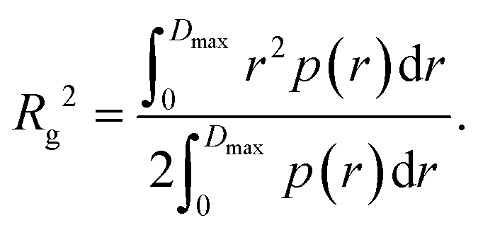
Furthermore, the pair distance distribution function p(r) (pddf) was used to validate the results:
 | (3) |
The pddf is the distribution of distances between scatterers in a sample. An advantage of the pddf is that it takes the whole scattering curve into account and not only the first few data points as in Guinier's approximation. In the third step, we fitted the form factor P(q,R) using Matlab2017a (The MathWorks, Natick, MA, USA) for solid spheres. The form factor can be written as
 | (4) |
This approach also takes the whole curve into account and the fit curve can be compared to the experimental data.
Flow simulations
COMSOL Multiphysics 5.2a (COMSOL GmbH, Göttingen, Germany) was used to perform finite element method (FEM) simulations of the flow conditions in the microfluidic devices. The inlet channels were reduced in length in the model to reduce the computational time, but are long enough to ensure equilibrated flow and mixing profiles. Simulations were performed in the laminar flow regime, thus employing the time-independent Navier–Stokes-equation, and no-slip boundary conditions are used at the channel walls. FEM simulations shown here represent the protein experiments using the diffusion coefficients Dvim = 2.2 × 10⁻¹¹ m2 s−1 and DKCl = 1.84 × 10⁻⁹ m2 s−1. The diffusion coefficient for vimentin is an estimate of the upper bound, since it decreases along the channel as the protein assembles. A change in viscosity upon assembly is not included in our simulation, since viscometry measurements show that the viscosity increases only very little during the first seconds of the assembly process.50,51Results and discussion
Device characterization
Kapton was chosen as a “base line” for our comparison, because the material is well established for X-ray experiments.8–10,13,22,26,29 This is due to its low and well defined background signal and negligible radiation sensitivity. Thus, Kapton provides a number of advantages when used as window material. However, in a typical microfluidic chamber, Kapton films have to be glued or bonded to other materials, such as stainless steel plates,8–10,13,22 PDMS,26 or UV-curable adhesive,29 that are used for defining the channel geometry, because the material is not self-adhesive. Kapton film with an adhesive layer (“Kapton tape”) typically leads to a fairly strong background signal itself. An exception are devices produced by laser ablation directly in Kapton and bonded to thermo-sensitive Kapton,52 which require considerable efforts in fabrication. The COC devices we present here, by contrast, are made from one single material such that there are no (glued) interfaces between the layers. We bond the COC layers directly without using solvents or silanes and without an additional plasticization step.To benchmark the new devices and test if they are suitable for SAXS measurements in general and in particular for SAXS on weakly scattering protein, we here directly compare measurements in microfluidic devices comprising 70 μm COC windows or 16 μm Kapton windows (total thickness). As a defined test system, gold colloids were used and we performed the experiments at two different synchrotron beamlines to account for differences concerning primary setup geometry, beam intensity, beam size and detectors. Fig. 4a shows typical scattering curves of gold colloids in the two device types, measured at ID13, ESRF. An advantage of the beamline is the highly focused beam (2.7 × 1.7 μm2), which can be used to exactly map the microfluidic channel. The background subtracted scattering data in the COC device (green) and in the Kapton device (blue) agree very well, even concerning the scattering intensity values. To further benchmark the validity of the data, we performed an analysis of the pddf yielding a radius of R = 11.02 nm ± 0.15 nm. Furthermore, the form factor of solid spheres was fitted to the data (red solid line) and we obtain a radius of 10.55 nm ± 0.06 nm.
 | ||
| Fig. 4 Colloid scattering curves with corresponding form factor. (a) Gold colloids measured at the ID13 beamline (ESRF) in a device with a COC window (green) and a Kapton window (blue). The form factor for solid spheres was fitted to the data and we obtain R = 10.55 nm ± 0.06 nm (red line). (b) Gold colloids measured at the cSAXS beamline (SLS) in a device with a COC window (green) and a Kapton window (blue). The form factor for solid spheres was fitted to the data and we obtain R = 16.13 nm ± 0.03 nm (red line). | ||
The cSAXS beamline at SLS is optimized for SAXS, providing access to very low q-values. Again, the data curves for the COC and the Kapton device fall exactly onto each other, as shown in Fig. 4b. In this case, we used colloids with a radius of 15 nm. For these data, we were able to analyze the Guinier region at small q-values; we find a colloid radius of 17.88 nm ± 0.49 nm. The pddf yields a radius of 16.50 nm ± 0.04 nm and the direct fit R = 16.13 nm ± 0.03 nm (red line). From these experiments, using a simple model system as scatterers, we conclude that the COC devices are well suited for performing SAXS experiments in microflow.
Experiments at synchrotron sources, i.e. with limited available time and highly complex setups, require robust, long-lasting microfluidic devices. In our experience the COC devices are very reliable and outperform the UV-curable adhesive/Kapton devices. It is even possible to flush them by hand, i.e. at comparatively high pressure and little control, without breaking them. In combination with our sample holder (see Fig. S3†), the success rate for these devices is close to hundred percent. With respect to radiation damage, we observe a strong effect in the Kapton devices, which is, however, not due to the Kapton but to the UV-curable adhesive. In the COC devices the effect is much weaker. We will thus, in the future, investigate radiation resistance of the material in a more systematic way.
Protein in flow
In a next step, we use our COC devices for measurements on a more challenging system: the weakly scattering protein vimentin. Vimentin belongs to the family of intermediate filament (IF) proteins and is found in cells of mesenchymal origin. Together with actin filaments and microtubules, it forms a composite biopolymer network in the cytoplasm. In vitro, vimentin assembles from tetrameric subunits into extended filaments in a hierarchical manner upon the addition of KCl.53 Within the first seconds, lateral assembly of the tetramers leads to so-called unit length filaments (ULFs), followed by an elongation mechanism, which may take minutes to hours and leads to micrometer long filaments.21,54,55 As a critical KCl concentration for assembly at these high protein concentrations, 10 mM was previously identified.23 By contrast to previous experiments,21,23 we here realize fast mixing by strong hydrodynamic focusing of the central protein stream (see Fig. 3b).4,56 Thus, the width of the central stream is about 10 μm and the diffusion time scale of the KCl into the central stream is on the order of 10 ms. The rapid increase of the KCl concentration, as obtained from the FEM simulations, is presented in Fig. 5a. The color code of the individual data points corresponds to the positions in Fig. 2a and the data curves in Fig. 5b. The red curve shows the unassembled tetrameric state, whereas the green curve indicates the start of the assembly. We observe that the forward scattering I0 increases with increasing assembly time, indicating an increase in molecular weight and, thus, assembly. Furthermore, the scattering curves steepen as the assembly proceeds. This change can be interpreted as an increase in thickness of the rod-shaped scatterers, corresponding to the known lateral assembly step of vimentin and in agreement with previously published work.21,55 Notably, we capture very early time points in this particular experiment. | ||
| Fig. 5 Vimentin measurement in a COC device, performed at the cSAXS beamline, SLS. In total, four different positions (see Fig. 2a) in the scanned device are shown. (a) The KCl concentration along the central channel is shown. The four analyzed positions are indicated by colored circles. Assembly starts at a KCl concentration of 10 mM. (b) The red data curve corresponds to tetrameric vimentin; the green data curve is defined as the starting point of the assembly process (t = 0); blue and purple data curves refer to slightly later, yet early, time points. | ||
Conclusions
To conclude, we present and characterize a microfluidic device fully made of COC. We demonstrate that the device is well-suited for X-ray measurements in flow. Weak SAXS signals from proteins, even of minute sample volumes, may be detected in a reliable, high-quality way. For benchmarking, we directly compare the performance of the COC devices to devices including Kapton windows. Aside from leading to SAXS data of equal quality, the COC devices provide a number of advantages over the UV-curable adhesive/Kapton devices. Above all, they are fabricated solely from one material, i.e. one type of COC without bonding layers, thus avoiding any gluing or interfaces, which are typically prone to leakage. Instead of plasticizing a thin layer on top of the COC sheet, we heat up the whole ensemble of two COC layers well above their glass transition temperature. As the unstructured sealing layer is much thinner (20 μm) than the structured main layer (240 μm) its viscosity decreases more rapidly, allowing for strong bonding. Indeed, the devices are more reliable than other devices we have tested here or in the past. Furthermore, COC materials have a high X-ray transmission and resist radiation. The device fabrication is straightforward and very reproducible at high quality, as it is already established for PDMS-glass devices. By contrast to commercial devices, as used for example in protein crystallography, the channel design is highly adaptable and flexible. Due to the employed lithography methods, the design of the microfluidic device can easily be customized. We believe that this approach will enable the community to perform various X-ray/microfluidics experiments in a very reliable way. Additionally, we are able to show that even weakly scattering protein signals may be investigated in this type of device. We thus expect a large number of different areas of application of these devices in the fields of biophysics, molecular biology and biochemistry.Conflicts of interest
There are no conflicts of interest.Acknowledgements
The authors thank Susanne Bauch for preparing the protein and TOPAS Advanced Polymers GmbH, Frankfurt, Germany, for providing the COC for the sealing layer. We furthermore thank Thomas Pfohl for helpful discussions. This work was financially supported by the Deutsche Forschungsgemeinschaft (DFG) in the framework of SFB 755, “Nanoscale Photonic Imaging”, projects B07 and C10, and the Cluster of Excellence and DFG Research Center “Nanoscale Microscopy and Molecular Physiology of the Brain” (CNMPB).References
- D. C. Duffy, J. C. McDonald, O. J. A. Schueller and G. M. Whitesides, Anal. Chem., 1998, 70, 4974–4984 CrossRef CAS PubMed.
- A. Ghazal, J. P. Lafleur, K. Mortensen, J. P. Kutter, L. Arleth and G. V. Jensen, Lab Chip, 2016, 16, 4263–4295 RSC.
- S. Köster and T. Pfohl, Mod. Phys. Lett. B, 2012, 26, 1230018 CrossRef.
- L. Pollack, M. W. Tate, N. C. Darnton, J. B. Knight, S. M. Gruner, W. A. Eaton and R. H. Austin, Proc. Natl. Acad. Sci. U. S. A., 1999, 96, 10115–10117 CrossRef CAS.
- L. Pollack, M. W. Tate, A. C. Finnefrock, C. Kalidas, S. Trotter, N. C. Darnton, L. Lurio, R. H. Austin, C. A. Batt, S. M. Gruner and S. G. J. Mochrie, Phys. Rev. Lett., 2001, 86, 4962–4965 CrossRef CAS PubMed.
- D. J. Segel, A. Bachmann, J. Hofrichter, K. O. Hodgson, S. Doniach and T. Kiefhaber, J. Mol. Biol., 1999, 288, 489–499 CrossRef CAS PubMed.
- S. Akiyama, S. Takahashi, T. Kimura, K. Ishimori, I. Morishima, Y. Nishikawa and T. Fujisawa, Proc. Natl. Acad. Sci. U. S. A., 2002, 99, 1329–1334 CrossRef CAS PubMed.
- T. Uzawa, S. Akiyama, T. Kimura, S. Takahashi, K. Ishimori, I. Morishima and T. Fujisawa, Proc. Natl. Acad. Sci. U. S. A., 2004, 101, 1171–1176 CrossRef CAS PubMed.
- T. Uzawa, T. Kimura, K. Ishimori, I. Morishima, T. Matsui, M. Ikeda-Saito, S. Takahashi, S. Akiyama and T. Fujisawa, J. Mol. Biol., 2006, 357, 997–1008 CrossRef CAS PubMed.
- M. Arai, E. Kondrashkina, C. Kayatekin, C. R. Matthews, M. Iwakura and O. Bilsel, J. Mol. Biol., 2007, 368, 219–229 CrossRef CAS PubMed.
- Y. Wu, E. Kondrashkina, C. Kayatekin, C. R. Matthews and O. Bilsel, Proc. Natl. Acad. Sci. U. S. A., 2008, 105, 13367–13372 CrossRef CAS PubMed.
- M. Arai, M. Iwakura, C. R. Matthews and O. Bilsel, J. Mol. Biol., 2011, 410, 329–342 CrossRef CAS PubMed.
- R. Graceffa, R. P. Nobrega, R. A. Barrea, S. V. Kathuria, S. Chakravarthy, O. Bilsel and T. C. Irving, J. Synchrotron Radiat., 2013, 20, 820–825 CrossRef CAS PubMed.
- R. Russell, I. S. Millett, M. W. Tate, L. W. Kwok, B. Nakatani, S. M. Gruner, S. G. J. Mochrie, V. Pande, S. Doniach, D. Herschlag and L. Pollack, Proc. Natl. Acad. Sci. U. S. A., 2002, 99, 4266–4271 CrossRef CAS PubMed.
- R. Das, L. W. Kwok, I. S. Millett, Y. Bai, T. T. Mills, J. Jacob, G. S. Maskel, S. Seifert, S. G. Mochrie, P. Thiyagarajan, S. Doniach, L. Pollack and D. Herschlag, J. Mol. Biol., 2003, 332, 311–319 CrossRef CAS PubMed.
- L. W. Kwok, I. Shcherbakova, J. S. Lamb, H. Y. Park, K. Andresen, H. Smith, M. Brenowitz and L. Pollack, J. Mol. Biol., 2006, 355, 282–293 CrossRef CAS PubMed.
- J. Lamb, L. Kwok, X. Qiu, K. Andresen, H. Y. Park and L. Pollack, J. Appl. Crystallogr., 2008, 41, 1046–1052 CAS.
- J. C. Schlatterer, L. W. Kwok, J. S. Lamb, H. Y. Park, K. Andresen, M. Brenowitz and L. Pollack, J. Mol. Biol., 2008, 379, 859–870 CrossRef CAS PubMed.
- R. Dootz, A. Otten, S. Köster, B. Struth and T. Pfohl, J. Phys.: Condens. Matter, 2006, 18, 639–652 CrossRef.
- T. Pfohl, A. Otten, S. Köster, R. Dootz, B. Struth and H. M. Evans, Biomacromolecules, 2007, 8, 2167–2172 CrossRef CAS PubMed.
- M. E. Brennich, J.-F. Nolting, C. Dammann, B. Nöding, S. Bauch, H. Herrmann, T. Pfohl and S. Köster, Lab Chip, 2011, 11, 708–716 RSC.
- S. Köster, H. M. Evans, J. Y. Wong and T. Pfohl, Biomacromolecules, 2008, 9, 199–207 CrossRef PubMed.
- O. Saldanha, M. E. Brennich, M. Burghammer, H. Herrmann and S. Köster, Biomicrofluidics, 2016, 10, 24108 CrossRef PubMed.
- O. Saldanha, R. Graceffa, C. Y. J. Hémonnot, C. Ranke, G. Brehm, M. Liebi, B. Marmiroli, B. Weinhausen, M. Burghammer and S. Köster, ChemPhysChem, 2017, 18, 1220–1223 CrossRef CAS PubMed.
- R. Stehle, G. Goerigk, D. Wallacher, M. Ballauff and S. Seiffert, Lab Chip, 2013, 13, 1529–1537 RSC.
- R. Dootz, H. Evans, S. Köster and T. Pfohl, Small, 2007, 3, 96–100 CrossRef CAS PubMed.
- M. Trebbin, D. Steinhauser, J. Perlich, A. Buffet, S. V. Roth, W. Zimmermann, J. Thiele and S. Förster, Proc. Natl. Acad. Sci. U. S. A., 2013, 110, 6706–6711 CrossRef CAS PubMed.
- H. Evans, R. Dootz, S. Köster and T. Pfohl, Bull. Pol. Acad. Sci.: Tech. Sci., 2007, 55, 217–227 CAS.
- B. Weinhausen and S. Köster, Lab Chip, 2013, 13, 212–215 RSC.
- J. Steigert, S. Haeberle, T. Brenner, C. Müller, C. P. Steinert, P. Koltay, N. Gottschlich, H. Reinecke, J. Rühe, R. Zengerle and J. Ducrée, J. Micromech. Microeng., 2007, 17, 333–341 CrossRef CAS.
- C. P. Steinert, J. Mueller-Diekmann, M. Weiss, M. Roessle, R. Zengerle and P. Koltay, 2007, IEEE 20th International Conference on Micro Electro Mechanical Systems (MEMS), 2007, pp. 561–564 Search PubMed.
- J. D. Ng, P. J. Clark, R. C. Stevens and P. Kuhn, Acta Crystallogr., Sect. D: Biol. Crystallogr., 2008, 64, 189–197 CrossRef CAS PubMed.
- S. Guha, S. L. Perry, A. S. Pawate and P. J. Kenis, Sens. Actuators, B, 2012, 174, 1–9 CrossRef CAS PubMed.
- M. Maeki, A. S. Pawate, K. Yamashita, M. Kawamoto, M. Tokeshi, P. J. A. Kenis and M. Miyazaki, Anal. Chem., 2015, 87, 4194–4200 CrossRef CAS PubMed.
- A. S. Pawate, V. Šrajer, J. Schieferstein, S. Guha, R. Henning, I. Kosheleva, M. Schmidt, Z. Ren, P. J. A. Kenis and S. L. Perry, Acta Crystallogr., Sect. F: Struct. Biol. Commun., 2015, 71, 823–830 CrossRef CAS PubMed.
- B. F. B. Silva, M. Zepeda-Rosales, N. Venkateswaran, B. J. Fletcher, L. G. Carter, T. Matsui, T. M. Weiss, J. Han, Y. Li, U. Olsson and C. R. Safinya, Langmuir, 2015, 31, 4361–4371 CrossRef CAS PubMed.
- S. A. Aghvami, A. Opathalage, Z. Zhang, M. Ludwig, M. Heymann, M. Norton, N. Wilkins and S. Fraden, Sens. Actuators, B, 2017, 247, 940–949 CrossRef CAS.
- T. I. Wallow, A. M. Morales, B. Simmons, M. C. Hunter, K. Lee Krafcik, L. A. Domeier, S. Sickafoose, K. Patel and A. Gardea, Lab Chip, 2008, 7, 1825–1831 RSC.
- F. I. Uba, B. Hu, K. Weerakoon-Ratnayake, N. Oliver-Calixte and S. A. Soper, Lab Chip, 2015, 15, 1038–1049 RSC.
- H. Cherdron, M.-J. Brekner and F. Osan, Angew. Makromol. Chem., 1994, 223, 121–133 CrossRef CAS.
- S. R. Quake and A. Scherer, Science, 2000, 290, 1536–1540 CrossRef CAS PubMed.
- H. Y. Park, X. Qiu, E. Rhoades, J. Korlach, L. W. Kwok, W. R. Zipfel, W. W. Webb and L. Pollack, Anal. Chem., 2006, 78, 4465–4473 CrossRef CAS PubMed.
- R. B. Urbani, Ph.D. thesis, Universität Basel, 2015 Search PubMed.
- H. Herrmann, L. Kreplak and U. Aebi, in Intermediate Filament Cytoskeleton, ed. M. B. Omary and P. A. Coulombe, Academic Press, 2004, ch. Method. Cell Biol., vol. 78, pp. 3–24 Search PubMed.
- B. Nöding and S. Köster, Phys. Rev. Lett., 2012, 108, 088101 CrossRef PubMed.
- S. Winheim, A. R. Hieb, M. Silbermann, E.-M. Surmann, T. Wedig, H. Herrmann, J. Langowski and N. Mücke, PLoS One, 2011, 6, 1–7 Search PubMed.
- R. Dinapoli, A. Bergamaschi, B. Henrich, R. Horisberger, I. Johnson, A. Mozzanica, E. Schmid, B. Schmitt, A. Schreiber, X. Shi and G. Theidel, Nucl. Instrum. Methods Phys. Res., Sect. A, 2011, 650, 79–83 CrossRef CAS.
- B. Henrich, A. Bergamaschi, C. Broennimann, R. Dinapoli, E. Eikenberry, I. Johnson, M. Kobas, P. Kraft, A. Mozzanica and B. Schmitt, Nucl. Instrum. Methods Phys. Res., Sect. A, 2009, 607, 247–249 CrossRef CAS.
- P. V. Konarev, V. V. Volkov, A. V. Sokolova, M. H. J. Koch and D. I. Svergun, J. Appl. Crystallogr., 2003, 36, 1277–1282 CrossRef CAS.
- H. Herrmann, M. Häner, M. Brettel, S. A. Müller, K. N. Goldie, B. Fedtke, A. Lustig, W. W. Franke and U. Aebi, J. Mol. Biol., 1996, 264, 933–953 CrossRef CAS PubMed.
- I. Hofmann, H. Herrmann and W. W. Franke, Eur. J. Cell Biol., 1991, 56, 328–341 CAS.
- R. Barrett, M. Faucon, J. Lopez, G. Cristobal, F. Destremaut, A. Dodge, P. Guillot, P. Laval, C. Masselon and J.-B. Salmon, Lab Chip, 2006, 6, 494–499 RSC.
- N. Mücke, T. Wedig, A. Bürer, L. N. Marekov, P. M. Steinert, J. Langowski, U. Aebi and H. Herrmann, J. Mol. Biol., 2004, 340, 97–114 CrossRef PubMed.
- C. G. Lopez, O. Saldanha, K. Huber and S. Köster, Proc. Natl. Acad. Sci. U. S. A., 2016, 113, 11152–11157 CrossRef CAS PubMed.
- H. Herrmann, H. Bär, L. Kreplak, S. V. Strelkov and U. Aebi, Nat. Rev. Mol. Cell Biol., 2007, 8, 562–573 CrossRef CAS PubMed.
- J. B. Knight, A. Vishwanath, J. P. Brody and R. H. Austin, Phys. Rev. Lett., 1998, 80, 3863–3866 CrossRef CAS.
Footnotes |
| † Electronic supplementary information (ESI) available: Extended version of Fig. 1, details on device fabrication, channel cross section and sample holder. See DOI: 10.1039/c7lc00824d |
| ‡ These authors contributed equally to this work. |
| This journal is © The Royal Society of Chemistry 2018 |