 Open Access Article
 This Open Access Article is licensed under a Creative Commons Attribution-Non Commercial 3.0 Unported Licence
Investigation of modified nanopore arrays using FIB/SEM tomography†
Angelika
Holzinger
a,
Gregor
Neusser
a,
Benjamin J. J.
Austen
b,
Alonso
Gamero-Quijano
c,
Grégoire
Herzog
 c,
Damien W. M.
Arrigan
b,
Andreas
Ziegler
d,
Paul
Walther
d and
Christine
Kranz‡
*a
c,
Damien W. M.
Arrigan
b,
Andreas
Ziegler
d,
Paul
Walther
d and
Christine
Kranz‡
*a
aInstitute of Analytical and Bioanalytical Chemistry, Ulm University, Albert-Einstein-Allee 11, 89081 Ulm, Germany. E-mail: christine.kranz@uni-ulm.de
bCurtin Institute for Functional Molecules and Interfaces, Curtin University, Perth, Western Australia 6845, Australia
cLaboratoire de Chimie Physique et Microbiologie pour les Matériaux et l’Environment (LCPME), UMR 7564, CNRS-Université de Lorraine, 405 Rue de Vandoeuvre, 54600 Villers-les-Nancy, France
dZentrale Einrichtung Elektronenmikroskopie, Ulm University, Albert-Einstein-Allee 11, 89081 Ulm, Germany
First published on 23rd February 2018
Abstract
The investigation of electrochemical processes at the interface of two immiscible electrolyte solutions (ITIES) is of great interest for sensing applications, and serves as a surrogate to the study of biological transport phenomena, e.g. ion channels. Alongside e-beam lithography, focused ion beam (FIB) milling is an attractive method to prototype and fabricate nanopore arrays that support nanoITIES. Within this contribution, we explore the capability of FIB/scanning electron microscopy (SEM) tomography to visualize the actual pore structure and interfaces at silica-modified nanoporous membranes. The nanopores were also characterized by atomic force microscopy (AFM) using ultra-sharp AFM probes to determine the pore diameter, and using scanning transmission electron microscopy (STEM) and energy dispersive X-ray (EDX) spectroscopy, providing additional information on the elemental composition of deposits within the pores. Si-rich particles could be identified within the pores as well as at the orifice that had faced the organic electrolyte solution during electrochemical deposition. The prospects of the used techniques for investigating the interface at or within FIB-milled nanopores will be discussed.
Introduction
The interface between two immiscible electrolyte solutions (ITIES) is highly suitable for analytical applications, enabling both ion and/or electron transport and thus the detection of redox active and inactive analytes.1,2 In particular, ordered micro- and nanometer-sized ITIES using nanopipettes3,4 and solid-state supports such as membranes5–11 have gained significant importance.12,13 Similar to micro- and nanoelectrodes, sensing applications benefit from an enhanced mass-transport/higher charge transfer due to hemispherical diffusion compared to macroscopic electrodes or interfaces, reduced capacitive current and a reduced ohmic drop.14,15 The diffusional behavior through micro-and nanopores in ITIES is thereby an important factor, determining the mass transport and charge transfer processes. The diffusion processes have been studied using electrochemical measurements and the obtained results have been compared with theoretical values16–19 providing information on the location of the interface. It has been shown that the diffusion process at nanopores can be described as the sum of linear diffusion within the pores and radial diffusion behavior at both orifices of the pores,18,20 as diffusion occurs in both directions, facing the organic and the aqueous side, respectively.21 Other parameters that influence the location of the interface between the two immiscible solutions are related to the interaction between the organic and the aqueous solutions, whereby the orientation of the organic molecules towards the water and the orientation of the electrolyte molecules in both solutions are dependent on the solvents used.22 The interface between water and 1,2-dichloroethane (DCE), which is also used in the present study, was used for measurements at nanopipettes3 and nano-sized porous membranes.23 Additionally, the deposition of Pd-nanoparticles at the water/DCE interface was observed in situ using spatial scanning spectroelectrochemistry introduced by Izquierdo et al.24 Electrochemical processes at the interface were monitored while transferred analytes were recorded simultaneously using UV-visible spectroscopy with a micro-focused beam displayed parallel to the liquid/liquid interface. The same approach was also used for the study of Au deposition in an ITIES formed from the contact of aqueous and organic phase droplets.25 The authors could show that Au(I) was formed as an intermediate species in the reduction of AuCl4−, using X-ray fluorescence (XRF) and X-ray absorption fine structure (XAFS) spectroscopy. The reported achievable spatial resolution is in the range of 70 μm. Raman confocal microscopy was also coupled to cyclic voltammetry at μITIES to follow the transfer of ions from one phase to the other.26 A water immersion objective with a long working distance was used to focus the laser on the interface and a depth spatial resolution of 1–2 μm could be reached. Despite this improvement, the spatial resolution achieved with spectroscopic techniques is not sufficient for the localization of the liquid–liquid interface within nano-sized membranes.Besides standard microfabrication techniques i.e. deep reactive ion etching (DRIE)8 for microporous membranes used in ITIES measurements, e-beam lithography with reactive ion etching27 and focused ion beam (FIB) techniques are highly attractive to fabricate solid-state nanopores and nanopore arrays in various 2D materials.28–30 FIB has been used as fabrication route for pore arrays supporting micro- and nanointerfaces milled in thin silicon nitride (SiN) membranes,31 as the pore-to-pore distance can be readily adapted. FIB prototyping has further advantages such as obtaining tunable nanopore array geometries, omitting multiple fabrication steps and modifying commercially available silicon nitride membranes with varying thicknesses. FIB milling is not limited to SiN membranes and other substrates, e.g., porous alumina32 have also been structured. Pores with diameters of 10 nm and less can be fabricated by additional treatments such as low pressure chemical vapor deposition of additional silica to FIB-milled nanoporous SiN membranes33 or by (cold) ion beam sculpting.28,30 FIB milling results in a truncated cone-shaped geometry of the pores due to re-deposition of milled material.28,34,35
Previous results and calculations for ITIES in nanopore arrays produced using e-beam lithography predicted that the pores are filled with the organic phase.36 Hence, the pore walls should be hydrophobic in nature. Experimental evidence is based on cyclic voltammetry, which provides information on the diffusional behavior, and on contact angle27 measurements, which determine the hydrophilicity of both sides of the porous membrane. However, contact angle measurements fail on the nanopore arrays like those investigated in the current study, as this method cannot be used for characterization of the inner pore walls. For alumina membranes, electrochemical studies at the water/DCE interface indicated that the pores are filled with the aqueous phase, through the location of deposited nanoparticles at the interface.37 Similarly, the pores of silicalite membranes were shown to be filled with the aqueous phase, using a facilitated ion transfer process with size-dependent exclusion of a ligand molecule due to the pore dimensions.38 For FIB-milled membranes, implanted Ga+ ions39 may influence the hydrophobicity of the pores’ inner walls, which in turn may influence the location of the liquid/liquid interface within the pore. Hence, exploring the characteristics of arrayed nanointerfaces produced using FIB milling is essential in order to understand the ion transfer at such interfaces. The truncated cone shaped geometry may be used to investigate the location of the interface when either the larger or smaller orifice of the pores is facing the organic electrolyte or aqueous electrolyte, respectively. Hence, pore arrays were FIB-milled from the front-side or back-side of the membrane within this contribution. The ion transfer at the back-side milled arrays with the smaller pore orifices facing the aqueous phase should be decreased due to a smaller interface than the ion transfer at the front-side arrays with larger orifices facing the aqueous phase, as long as the diffusion zones at adjacent pores are not overlapping. Recently, Liu et al. have shown that the diffusional behavior of nanopore arrays with different pore-to-pore spacing can be visualized via the deposition of silica and using AFM-scanning electrochemical microscope measurements.40 Depending on the pore spacing, overlapped diffusion profiles at arrays with smaller pore–pore distance or independent diffusion profiles at arrays with larger pore center-to-center separations lead to a large silica deposit covering the whole array, or individual deposits at the pores, respectively. However, no information on the behavior within the pores nor on the location of the interfaces was retrieved from these studies.
To visualize the pore shape and inner pore space of SiN membrane-supported nanopores, high-resolution transmission electron microscopy (TEM) tomography has been employed.41,42 In contrast to TEM, FIB/SEM tomography43 enables the reconstruction of large sample sections with a resolution down to several nanometers.44,45 FIB-milled cross-sections of nanopores have been published by Liu et al. in order to investigate the shape of the nanopores, especially with respect to electron- or ion beam-induced shrinking.34 Using repeated FIB sectioning and SEM imaging of the freshly prepared face, not only the morphology but also the pore volume and interconnectivity of porous material can be reconstructed, providing three-dimensional information in the micro- and nano-range. 3D FIB/SEM investigations have been demonstrated for biological samples, e.g. cells, providing structural information on membranes,46 for molecular imprinted polymers, for investigating pore connectivity47 and for materials related studies of the inner structure of Al–Si alloys48 or arrays of metal nanotubes.49
The aim of this work was to investigate the location of the interface of FIB-milled nanopores using high-resolution inspection of deposited silica. These studies have revealed that processes occur also within the pores. Within this contribution, we employ FIB/SEM tomography as an innovative method to study the modification of nanopores and specifically the interior of the pores in an ex situ, post-deposition approach. This provides 3D information on the electrochemically deposited silica at nanoporous arrays as solid-state supports for ITIES measurements. Information is also gained about the truncated geometry of the nanopores by 3D reconstructions. For silica deposition, tetraethoxysilane (TEOS) is used as the silica precursor, which is located in the aqueous phase, while cetyltrimethylammonium (CTA+) is the template molecule dissolved in the organic phase.50 The ion transfer of the template CTA+ from the organic to the aqueous phase leads to the condensation of silica on the aqueous side of the interface. The location of the silica might give information about the location of the ITIES during deposition. By forming a solid phase at the interface of the immiscible solutions, the location of this interface can be visualized, as has been shown for Pd deposition at alumina membranes.37 For the silica deposits studied here, the pores’ interior is analyzed using EDX and STEM measurements, an example of which is shown in Fig. 1.
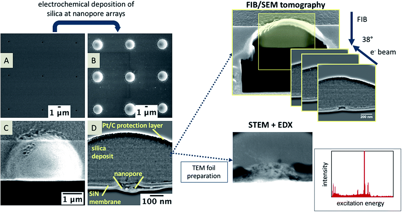 | ||
| Fig. 1 An overview of nanopore modification and the used techniques for the investigation of silica modified nanopore arrays. SEM images of a FIB-milled nanopore array before (A) and after (B) electrochemical deposition of silica. For 3D FIB/SEM tomography, the silica deposit is coated with a Pt/C layer and cross-sectioned using FIB (C), with the sample tilted to 52° so that the sample surface is perpendicular to the ion beam. After each milling step, a SEM image is taken of the in-plane area of the silica deposit, which is exposed using FIB sequencing. Due to the tilt correction in the y-axis, the SEM images appear under an angle of 38° (D). | ||
Experimental
Materials and methods
Nanopore arrays were fabricated in SiN membranes (50 and 100 nm DuraSiN Films, Protochips, Inc., Science Services) via FIB milling (30 kV, 1.5 and 10 pA, using a dual beam FIB/SEM FEI Helios Nanolab 600, ThermoFisher Scientific) with varying pore diameters and pore-to-pore separations sufficient to ensure individual pore diffusion51 during electrochemical deposition of silica. AFM (5500 AFM/SPM microscope, Keysight Technologies) was used to characterize the pore shapes of the individual nanopores in dynamic mode AFM with a FIB-sharpened NCL probe (k = 48 N m−1, 190 kHz, Nano World).Electrochemical deposition of silica
The electrochemical silica deposition at the nanopores was obtained as previously reported by Poltorak et al.50 Briefly, a sol of 50 mM of TEOS was prepared in 5 mM NaCl and the pH was adjusted to pH 3 by addition of aliquots of 1 M HCl. The sol was stirred for 90 minutes at room temperature to allow hydrolysis to occur (Fig. S1†). The ethanol produced by the hydrolysis was removed using evaporation and the pH was raised to 9 by the addition of aliquots of 1 M NaOH solution (unless stated otherwise). An electrochemical cell was built with the obtained sol as the aqueous phase, as follows: Ag|AgCl|50 mM hydrolyzed TEOS + 5 mM NaCl (aqueous)‖14 mM CTA+ TPBCl− (DCE)|Ag. The template salt was prepared by metathesis from K+TPBCl− (potassium tetrakis(4-chlorophenyl)borate) and CTAB (cetyltrimethylammonium bromide) as described elsewhere.52 The interfacial potential difference was controlled by a PGSTAT 302N potentiostat (Autolab, Metrohm). A potential of −0.1 V or 0 V was applied for 30–60 s. At this potential, CTA+ is transferred from the organic to the aqueous phase, triggering the condensation reaction between silanol groups to form Si–O–Si bonds. After the electrochemical deposition step, the membrane was carefully removed from the solution and rinsed with a flow of ultrapure water (18.2 MΩ cm, Purelab OptionQ, Elga water purification system) to avoid any formation of silica through evaporation. The membranes were then placed in an oven at 130 °C for 16 h to ensure cross-linking.FIB/SEM tomography
Prior to tomography, the silica-modified samples were modified with a thin Pt layer (3–4 nm) to prevent charging effects during the milling and imaging steps using sputter coating (SCD 005, BAL-TEC). Additional Pt/C deposition using ion beam induced deposition (IBID, precursor: methyl-cyclopentadienyl-trimethyl platinum) stabilizes and protects the sample and the silica deposits during TEM foil preparation and FIB/SEM tomography. Tomography was performed with the ‘slice and view’ software package (FEI, ThermoFisher Scientific) with automated FIB milling steps of the sample at 30 kV acceleration voltage and 1.5–48 pA beam current. Slices with a thickness of 5 or 10 nm were FIB-milled; a SEM image is recorded after each milling step at 5 kV and 86 pA with the through-the-lens (TLD) detector.TEM lamella preparation
TEM foils were prepared as described in detail elsewhere.53 Briefly, a small lamella with a thickness of approx. 1 μm of the membrane containing the silica-modified nanopore is isolated through several FIB milling steps and attached via IBID to the micromanipulator needle (Omniprobe) (see ESI Fig. S2†) and removed from the sample. This small lamella is then transferred onto a Cu TEM grid (Omniprobe), fixed with IBID, and thinned using FIB to a thickness of approximately 150–200 nm. TEM images were recorded at 120 kV (EM 912 TEM, Zeiss); STEM and EDX measurements were performed using a FE-SEM (S-5200, Hitachi) operated at 30 kV acceleration voltage, equipped with a Phoenix (EDAX) X-ray detector and a STEM detector.Data processing
The recorded AFM images and corresponding height profiles were processed using PicoView (Keysight Technologies). The recorded slices of the FIB/SEM tomography were processed by Fiji.54 The images were aligned using ‘linear stack alignment with SIFT’,55 followed by the application of a FFT bandpass filter to adjust the brightness and contrast for all recorded and processed slices. 3D graphs were obtained with Avizo 9.1.0 Lite (FEI, ThermoFisher Scientific).Results and discussion
Silica deposition at FIB-milled nanoporous arrays with truncated cone-shaped geometry
It is known that pores fabricated using FIB are typically characterized by a truncated cone-shaped geometry.28,34,35 Prior to the modification with silica, the nanopores were characterized using AFM with respect to the pore shape using an ultra-sharp AFM tip. Membranes with a thickness of 100 nm were investigated, which were milled either from the front or the back-side, using the same FIB milling parameters. The influence of the truncated shape and the orientation of the truncated geometry towards either the aqueous or the organic electrolyte solution has already been shown for microporous glass membranes fabricated using laser ablation.9 Microporous arrays with defined hydrophobicity of the inner pore walls, determined using contact angle measurements, have been presented. The interface location and a hemispherical shape of the interface could be identified due to the diffusional information gained from cyclic voltammetry and corresponding simulations. To the best of our knowledge, this is the first time that FIB-milled nanopores with a truncated cone-shaped geometry are compared with respect to their orientation towards immiscible electrolyte solutions during electrochemical silica deposition (Fig. 2A). Fig. 2B and C summarize the results of the AFM characterization of the pore geometry and pore diameter prior to the deposition. An ultra-sharp AFM tip, obtained using FIB milling, was used for imaging (Fig. 2D). During sharpening of the tip, the 9 degree mounting angle of the AFM cantilever towards the membrane’s surface was taken into account. Therefore, the V-shaped truncated form of the front milled nanopore can be imaged (see extracted depth profile, dark blue line, Fig. 2C). For the back-side milled nanopores, only the pore diameter of the small orifice can be mapped. The depth profile of the back-side milled pore (light blue line, Fig. 2C) represents the geometry of the ultra-sharp AFM tip and not the actual pore shape (as clearly seen from the scheme shown in Fig. 2A).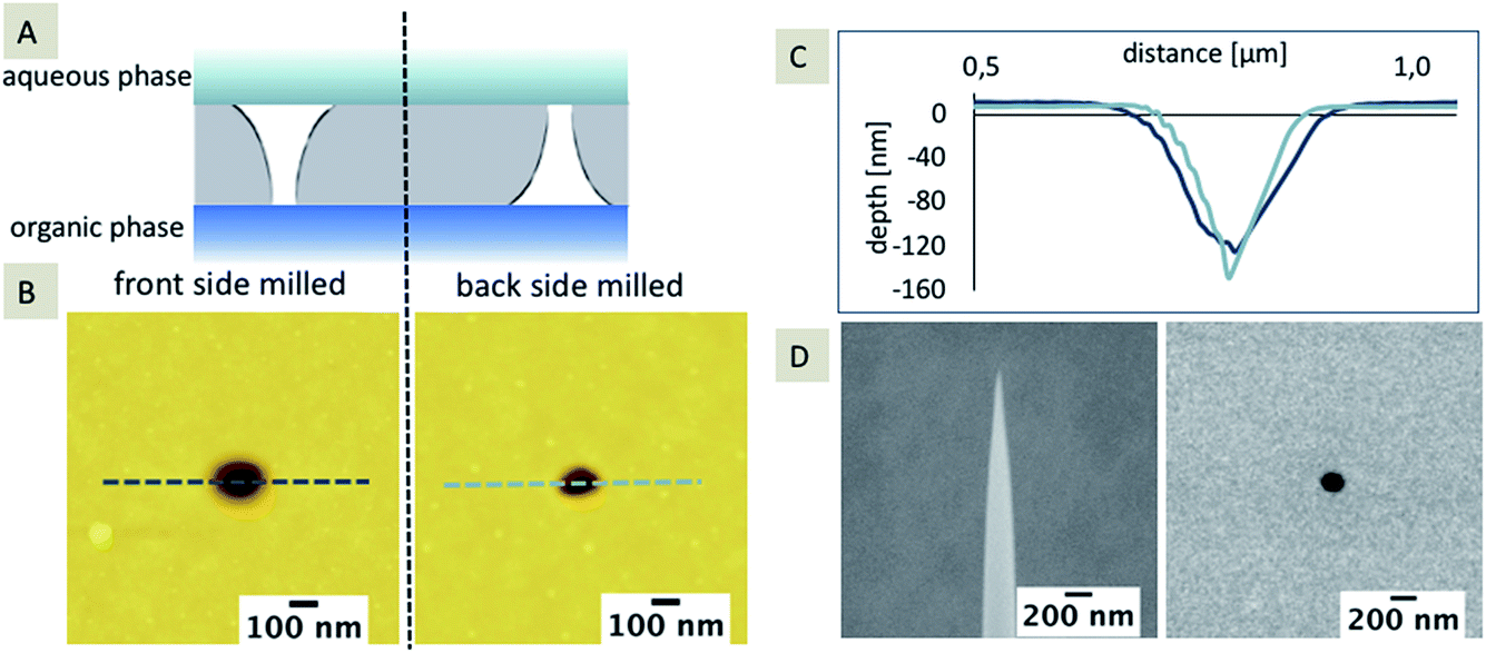 | ||
| Fig. 2 Scheme of the orientation of the truncated cone-shaped pore towards the immiscible electrolyte solutions for front and back-side milled arrays (A). Dynamic mode AFM topography (B) of a single pore of a pore array fabricated from the front-side (B, left) or back-side (B, right) FIB milling and corresponding cross-sectional profiles (C) extracted at the marked lines: 152 kHz (A)/169 kHz (B). Images were recorded with a scan speed of 1 ln/s (A, B). SEM images of a high-aspect AFM tip (D, left) and of a single pore of a pore array with a center-to-center separation of rc > 150 rpore (D, right). | ||
The average pore diameter measured using AFM is 183 nm ± 29 nm (n = 3) for the front-side milled and 72 nm ± 12 nm (n = 3) for the back-side milled arrays, respectively. The pore diameter determined using SEM is on average 151 nm ± 14 nm (n = 100, front-side milled). As the membrane is located on a frame with a 300 μm thickness, FIB milling and SEM imaging of the back-side of the SiN membrane is less accurate, which results in a slightly distorted pore diameter as determined using SEM. Therefore, the diameter determined using SEM for the back-side milled array is not taken into account. In addition, the diameter of the small orifice could not be determined via SEM without destroying the membrane. The overall small discrepancy in average diameter (determined using AFM and SEM) observed for the front-side milled pores may be explained by the limited number of measurements for AFM and, more importantly, by the limitations of SEM in providing pure surface information.44 In addition, TEM tomography also reveals the conical pore shape (see ESI, Movie 1†).
The dimensions of the silica deposits at these two SiN membranes, milled from either the front-side or the back-side of the membrane, should give information about the influence of the FIB milling on the hydrophobicity of the pores. In general, the location of the interface, and hence the hydrophobicity influences the diffusion and the formation of the silica deposits. If the interface is inlaid on the aqueous side (organic phase fills the pore), the diffusion should be more rapid (radial diffusion) compared to a fully recessed interface (aqueous phase fills the pore), leading to linear diffusion. As a result, the silica deposits should be larger for the inlaid case or smaller for the recessed case, given that the pore sizes are the same and the pores are cylindrical. If the pore orifices are different, then the effects will be altered and the diffusion at conical pores is governed by three pore-related factors, which in turn influence the silica deposition: (1) interface location – recessed or inlaid; (2) interface size (radius), and (3) pore shape (cylinder, cone, or inverted cone). In the case, the FIB-milled conical pores are filled with the organic phase as shown for SiN membranes fabricated by e-beam lithography27 and assumed for FIB-milled membranes,31 the interface is located at the orifice on the aqueous side of the membrane. As the orifice facing the aqueous electrolyte differs in size for the front-side and back-side milled membranes (Fig. 2B), the silica deposition should be larger at the front milled pore array compared to the back milled array. In Fig. 3A, the results for the silica deposition at two arrays of 100 nanopores (front and back-side milled) show different sizes of the silica deposits for both approaches, which are randomly distributed. By comparison of the different diameters of the silica deposits, the back-side milled sample interestingly shows deposits with larger diameters of up to 10 μm (Fig. 3B), which is indicative of enhanced ion transport.
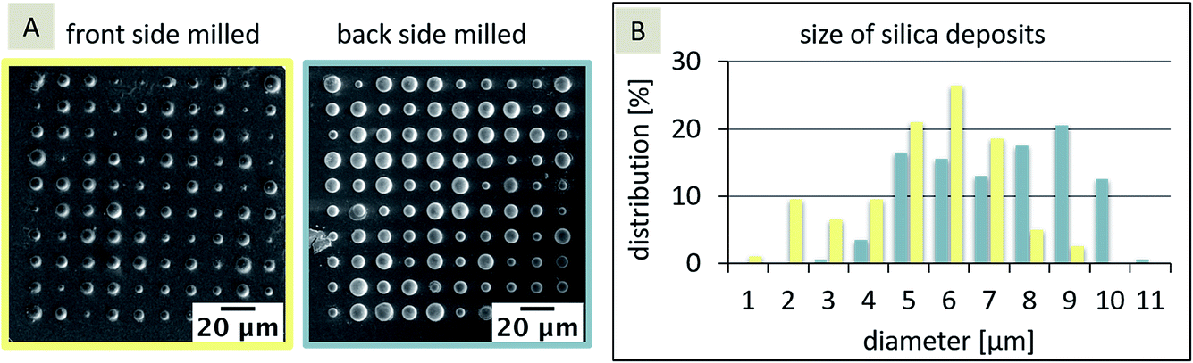 | ||
| Fig. 3 SEM images of silica deposits at the front-side (A, left) and back-side (A, right) milled nanoporous arrays with the size distribution of the silica deposits for the front-side milled (yellow) and the back-side milled (blue) approach (B). Deposition occurred at 0 V vs. quasi Ag/AgCl reference electrode at pH 9. | ||
In the first step, a paired two-tailed t-test with a 95% confidence level was applied, which revealed that the variation of the silica deposits for front-side and back-side milled arrays is significant. Table 1 shows the diameters and respective standard deviations determined within the individual arrays.
| Pore diameter determined using AFM (n = 3; mean value ± SD) | Pore diameter determined using SEM (n = 100; mean value ± SD) | Diameter of silica deposits determined using SEM (n = 100; mean value ± SD) | |
|---|---|---|---|
| front-side milled | 183 nm ± 29 nm (large orifice) | 151 nm ± 14 nm, SD equals 17% of the mean value | 5.3 μm ± 3.0 μm, SD equals 57% of the mean value |
| back-side milled | 72 nm ± 12 nm (small orifice) | 170 nm ± 14 nm, SD equals 16% of the mean value | 7.4 μm ± 3.2 μm, SD equals 43% of the mean value |
The standard deviation of the silica deposits (43% and 57% of the mean value for diameters, respectively) within one array is evidently larger than the difference between the silica deposits at the two arrays. Interestingly, the initial pore sizes of the two arrays had only small standard deviations (16 and 17% of the mean value, respectively). As a result, an unambiguous interpretation of the location of the interface is challenging. It has been shown that osmotic pressures or double layers within the nanopores influence the ion transfer at truncated pores, even for miscible solutions. This also leads to an ion current rectification depending on the ion flow direction within the truncated cone-shaped geometry.56 In the next step, FIB/SEM tomography was evaluated as method to obtain information about silica deposits. In principle, silica is formed in the aqueous phase,50 following the electrochemical ion transfer of the template CTA+ from the organic to the aqueous phase. TEOS, which is the precursor of silica via hydrolysis and condensation, is only present in the aqueous phase.
FIB/SEM tomography
The location of the silica deposit at or in the pore after the electrochemical deposition may indicate the location of the interface. Along with the characterization of the deposits formed outside the pores, FIB/SEM tomography can also reveal information about the insides of the pores. Pores from an array with an average pore diameter of 72 nm ± 12 nm (n = 3, back-side milled) were investigated, which were modified with silica via applying a constant potential of 0 V vs. quasi Ag/AgCl reference electrode for 90 s at pH 9. Fig. 4A shows the FIB-induced secondary electron (SE) image (top view) of a single cross-sectioned silica modified pore stabilized with Pt/C to prevent charging effects during milling and imaging. The SEM images in Fig. 4B–E provide a side view at 38° (tilt corrected). Fig. 4B and D reveal the dense inner structure of the silica deposit whereas Fig. 4C and E show the cross-sections of deposits at two different pores of the back-side milled array. The SEM images clearly indicate that silica has been deposited onto the membrane on the aqueous side, but also that some residue is visible within the pore and at the organic electrolyte-facing side of the membrane. The morphology of the deposits is quite different on both sides of the membrane. While the silica deposit located on the aqueous electrolyte facing side of the membrane consists of a dense homogeneous structure, the pore inside appears to be filled with a single particle and other debris (see Fig. 4C and E). The variation of contrast in the SEM image indicates an inhomogeneous composition of this mixed structure within the pore and at the organic facing side of the membrane, referred to as “residue” in the following text. The silica deposit shown in Fig. 4E appears as dense material, although two different areas can be identified based on the imaging contrast. A hemispherical region located at the pore orifice indicates a denser structure displayed as dark grey in the SE contrast (Fig. 4E, marked with arrows) and an adjacent area with lighter contrast. This hemispherical geometry is due to the diffusion of the template from the nanopore to the aqueous phase during silica deposition. In close proximity of the pore and the interface, the hemispherical diffusion is increased and silica is quickly deposited, leading to the observed contrast in the SE image. Also, a gap, visible between the silica deposits and the SiN membrane, was observed (Fig. 4D and E). Such gaps were predominantly visible at silica deposits larger than 9 μm in diameter. The gap might be related to the drying process, which involves a shrinking of the silica due to solvent loss, although it is not observed for all deposits (see Fig. 4B and C). It has to be noted that the removal of the electrolyte solutions, and further cleaning/drying steps of the silica deposit may have also an effect.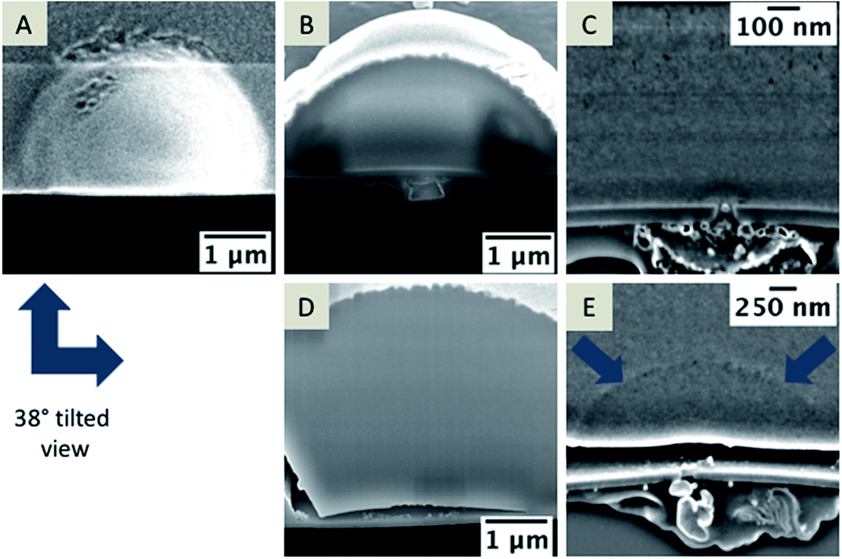 | ||
| Fig. 4 FIB-induced SE image of a silica deposit coated with Pt/C and partially FIB-milled, (top view) (A) and a SEM image of a cross-section of the silica deposit, with a tilt-corrected view at an angle of 38° (B–E). SEM images of silica deposits with diameters smaller than 5 μm (B and C) or larger than 9 μm (D and E). Cross-sections of the silica deposits shown in B and D were recorded after FIB/SEM tomography (B) and before FIB/SEM tomography (D). Hence, the pores and the residues at the organic facing side are not visible in (B and D). | ||
An example 3D reconstruction of a FIB/SEM tomography is depicted in Fig. 5 with a corresponding series of SEM images from the tomography stack (Fig. 5A, I–IV; the complete tomography stack is given in Movie 2†). The 3D reconstruction (Fig. 5B) reflects the residue, which is located around the pore orifice facing the organic electrolyte during electrochemical deposition, and an inhomogeneous structure inside the pore partially connected to the silica deposit. The drop-like structure below the membrane shows a high porosity, which seems also to be encapsulated by a thin layer (colored in yellow in the 3D reconstruction shown in Fig. 5B). This layer is visible across the entire membrane on the organic facing side, whereas the drop-shaped residue is just located close to the nanopore. Differentiation of independent structures or particles in the SE contrast is difficult. Also, discrimination between the in-plane area and the sample volume is not possible at these dimensions in the nanometer range due to the penetration depth of the electron beam.44 However, the conical pore shape is clearly evident within the 3D reconstruction. Further information about the elemental composition of the deposit at the organic electrolyte facing side was obtained using EDX mapping from a thin TEM foil (for details see Fig. S2 and S3†).
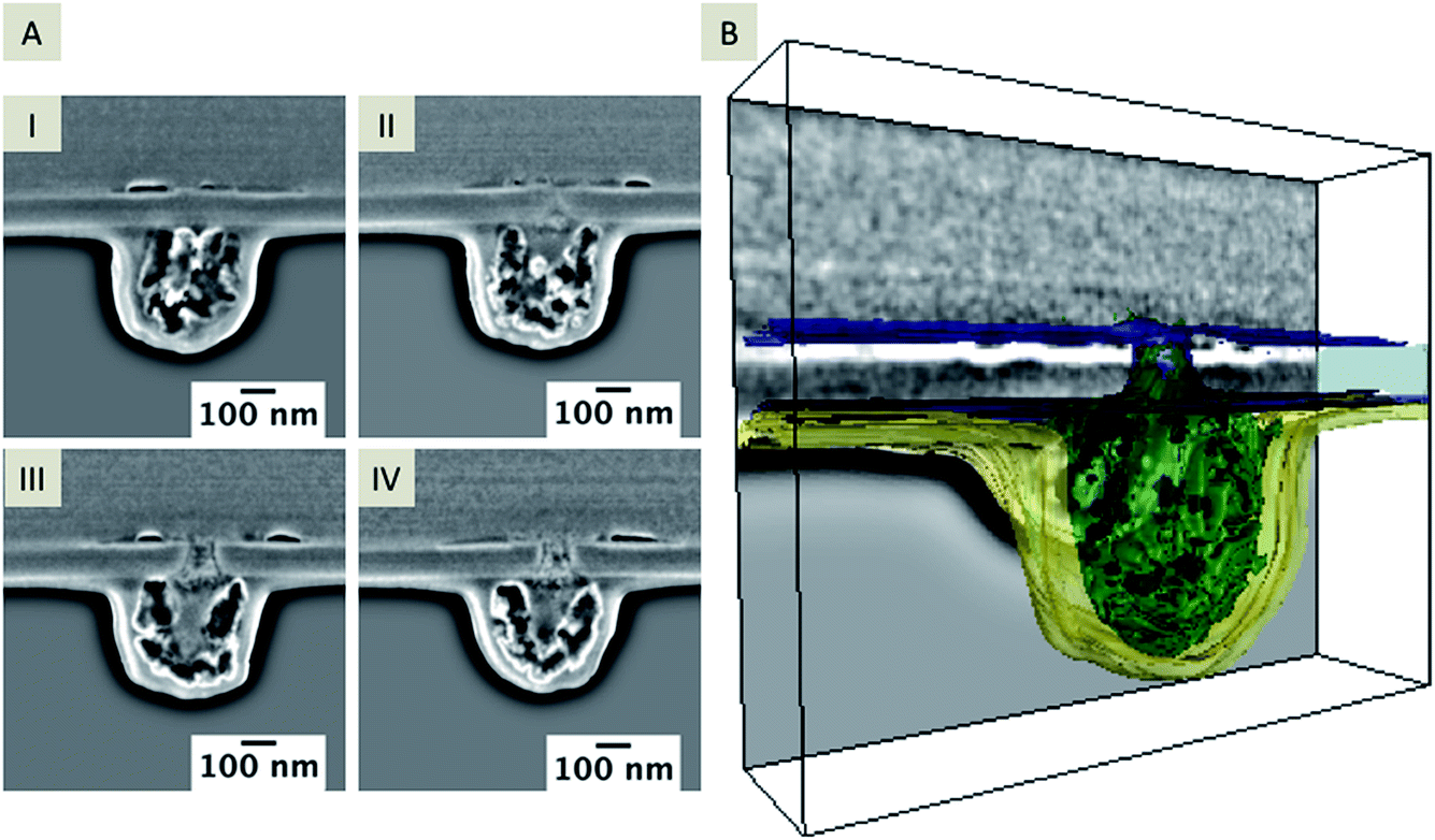 | ||
| Fig. 5 Extracted SEM images of a FIB/SEM tomography stack showing the deposit on the nanopore and the deposit that was formed at the orifice facing the organic side. The distance between single slices is 30 nm, the acceleration voltage is 5 kV and the current is 86 pA, depicted at a 38° tilt (A, I–IV). A 3D reconstructed pore showing the deposits located at the organic facing side and within the nanopore (B) according to the entire stack, which is given in ESI Movie 2.† | ||
Investigation of the elemental composition
In Fig. 6A, a TEM image of a nanopore is depicted and a bright particle within the pore can be seen in the magnified area marked with a blue circle. The TEM foil was flipped vertically for EDX mapping (Fig. 6B). The EDX data clearly show that Si-containing material is also located at the organic electrolyte facing side (Fig. 6C). Si should be just located in the aqueous phase, either as Si(OH)4 or as silica. For elemental mapping of the pore content, it is important that the TEM foil contains an area of the sample where the pore is open from both sides (see scheme in Fig. 7).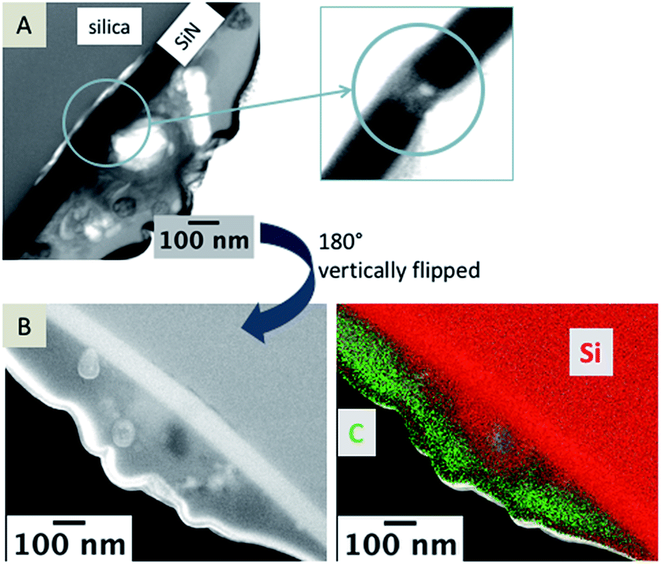 | ||
| Fig. 6 TEM images of a nanopore (A) and a magnified view of the pore. A SEM image of the TEM foil (B), vertically flipped by 180°; and EDX mapping of the area; false color image showing carbon in green and silicon in red (B, right). Complete data for the EDX mapping is given in the ESI, Fig S3.† | ||
It is necessary to discriminate between signals of the observed in-plane area exposed from FIB milling and the sample volume, as EDX and SEM are sensitive towards the subsurface composition with excitation depths larger than the thickness of the investigated TEM foils.44 As shown in the corresponding SEM image (Fig. 6B), the nanopore is not visible but it is contained within the sample volume of the TEM foil. Therefore, the EDX signals within the pore are overlaid by the signal of the SiN membrane and no information is gained about the elemental composition of particles and residues located within the pore, which are visible in the TEM image (Fig. 6A).
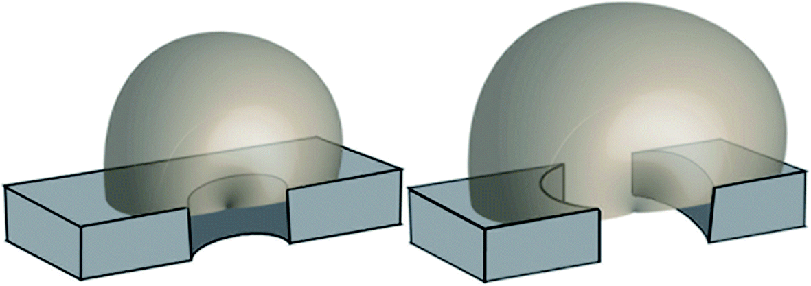 | ||
| Fig. 7 Scheme of modified nanopores with a small (left) and large (right) pore diameter. For pore diameters larger than the thickness of the prepared TEM foil, the pore is accessible from both sides of the TEM foil. | ||
In case of small pore diameters (72 nm ± 12 nm), such as for the pore shown in Fig. 6, it is rather challenging to prepare a TEM lamella that contains a single pore, which is open from both sides, as illustrated in Fig. 7. The achievable thickness of the TEM foil is limited57,58 and the minimum thickness of the TEM samples fabricated within this study was approximately 150–200 nm. To overcome these limitations, nanopore arrays with pore diameters of 250–350 nm were FIB-milled, which is sufficient to prepare a TEM foil containing a single pore that avoids the problem of convolution of the EDX data of the pore content and the SiN membrane. These nanopore arrays were FIB-milled from the front-side of the membrane (thickness of the SiN membrane: 50 nm); this front-side was subsequently in contact with the aqueous electrolyte solution during electrochemical deposition. Two example nanopores of the investigated arrays are shown in Fig. 8 after silica deposition. The electrochemical formation of silica was performed at pH 9 (Fig. 8A and B) and also tested at pH 3 (Fig. 8C) using different deposition times at the two pH values.
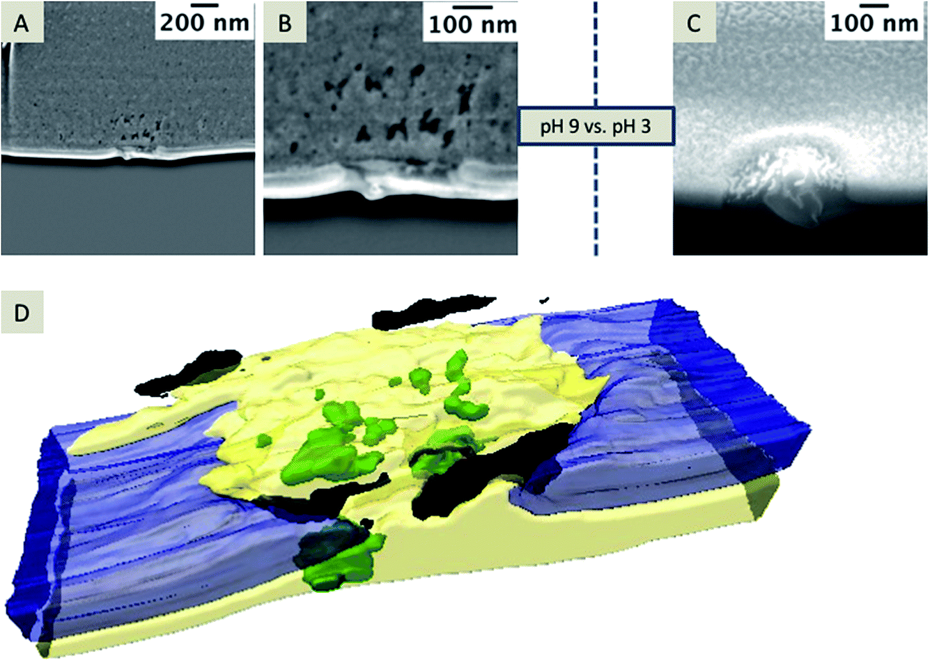 | ||
| Fig. 8 SEM images of the deposits formed at pH 9 (A, and magnified view shown in B, applied potential for deposition is −0.1 V for 60 s) and at pH 3 (C; applied potential is −0.1 V for 30 s), with an acceleration voltage of 5 kV and current of 86 pA, depicted at a 38° tilt. A 3D reconstruction of the FIB/SEM tomography of the silica formed at pH 9 (SEM images shown in A and B are single slices of this stack) is depicted in (D). The entire stack is given in the ESI Movie 3.† | ||
At pH 9, the transport of CTA+ is strongly facilitated and highest as the polynuclear species (Si4O6(OH)62−) and (Si4O8(OH)44−) are predominant in the aqueous phase.59 Hydrolyzed TEOS polycondensates around CTA+ ensembles to form the silica. At pH 3, mononuclear species of Si(OH)4 are dominant, which may not facilitate the transfer of CTA+ to the aqueous phase and therefore silica deposits should be absent at or within the nanopores.52 To exclude the idea that the observed Si-rich residue within the pore or at the organic electrolyte facing side is related to silica removed from the deposits during rinsing, cleaning or drying, experiments were performed at low pH. As expected, the electrochemical deposition at pH 3 (Fig. 8C) does not lead to silica formation as observed at pH 9 (Fig. 8A and B). However, some pores are filled with solid particles (2 of 3 measured pores contained solid material) embedded in the residue filling the nanopore (Fig. 8C). In Fig. 8A and B, a randomly mixed phase obviously composed of different materials, according to the contrast of the SEM image, is visible. Single particles are labeled as green in the 3D reconstruction (Fig. 8D and Movie 3 in the ESI†). The black areas in the reconstruction reflect “holes” within the residue. The entire residue, which cannot be identified as holes or particles due to insufficient contrast in the SE image, is depicted in yellow.
Also, a nanoporous array, which was used in experiments with an acidic aqueous phase, was investigated. Although, it is not expected that silica deposits will be formed at pH 3, a modification of the pores was observed. After preparing a TEM foil with a pore as schematically shown in Fig. 9A–C, EDX analysis was performed.
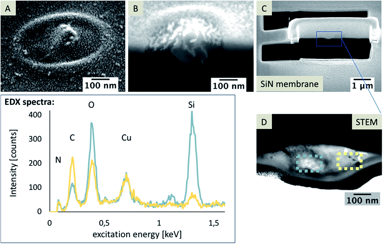 | ||
| Fig. 9 SEM images of a nanopore after electrochemical modification with no expected silica formation at pH 3 (A) and after cross-sectioning of a filled nanopore (B). Images are shown at a 38° tilt, with an acceleration voltage of 5 kV and current of 86 pA. A TEM lamella with additional Pt/C layer (C) and a STEM image of the pore (30 kV, D); EDX spectra were recorded within the pore in areas marked by the blue and yellow square in (D). | ||
The EDX spectra shown in Fig. 9 clearly reveal that the bright spot recognizable in the STEM image (Fig. 9D, marked with a blue square) consists of Si. Other areas, e.g. that marked with a yellow square, mainly consist of oxygen and carbon. In both spectra, the detected Cu signal is related to the copper TEM grid. As no silica formation should be observed at pH 3, these Si-rich particles might be remains of the precursor TEOS. Another reason for these particles within the pores might be related to pre-concentration effects of the non-condensed Si(OH)4 during the removal of the electrolyte solution or drying, leading to a reduced volume and the formation of silica. If we assume that these particles are related to the aqueous phase with dissolved non-condensed Si(OH)4, the question arises as to why the Si(OH)4 containing phase is obviously also below the pore separated from the silica deposit and not condensed to silica, indicated by the Si-rich phase in the EDX map shown in Fig. 6. In general, the condensation of silica is faster in the presence of a template, hence Si(OH)4 should be condensed to silica directly in the ITIES at a suitable pH value. In close proximity of the silica deposits, these single Si-rich particles can be residues flushed or moved inside the pore while drying or cleaning. However, this would not explain the large residues observed at the organic electrolyte facing side, which are visible at most investigated pores and whose dimensions were significantly larger in the sample with small pore diameters of 72 nm ± 12 nm (n = 3) (Fig. 10A and B). It is unlikely that such particles were accidentally moved through the pore to the organic facing side of the membrane during cleaning or rinsing. Hence, it is hypothesized that these particles were formed either during electrochemical deposition or due to a pre-concentration of TEOS in the post-deposition steps as described above. These residues are also evident at pore arrays with large diameters of 250–350 nm, as determined using AFM and SEM (Fig. 10C, AFM results not shown).
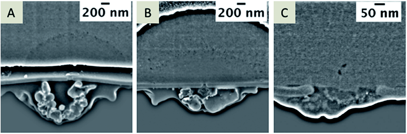 | ||
| Fig. 10 SEM images of different nanopores with small (72 nm ± 12 nm, A and B) and large (322 nm ± 84 nm, C) pore diameters with respect to the residue at the pore facing towards the organic electrolyte during electrochemical deposition. Recorded with an acceleration voltage of 5 kV and current of 86 pA, depicted at a 38° tilt. | ||
These observed particles may also be related to the silica forming chemistry. The hydrolysis of TEOS to silica forms ethanol as a side product.60 Ethanol is soluble in both water and DCE, which may lead to a mixed layer. To avoid the formation of that mixed layer at the interface, ethanol resulting from the hydrolysis was evaporated. Hence, these particles can be related to the aqueous phase located within the nanopores during electrochemical measurements or, less likely, be related to displaced particles moved into the pores during cleaning and drying.
Conclusions
Within this contribution, we demonstrate the potential of FIB/SEM tomography for investigating nanopore arrays with the aim of localizing the interface between two immiscible electrolyte solutions, more precisely the visualization of electrochemically deposited silica at nanoporous arrays. While mesoporous silica formation with a homogeneous appearance is observed at the aqueous electrolyte facing side, it appears that within the pores a random mixture of different phases has been detected from the FIB/SEM tomography studies. Interestingly, Si-rich areas within the pores were determined, which indicates that in the presented experiments the obtained pores may not be entirely filled with the organic phase. Regarding the rather high carbon content detected using EDX, it is assumed that a mixed phase within the pores was present in the specific example investigated herein. This hypothesis is also supported by the results obtained for front-side vs. back-side milled pore arrays, where no significant variation in terms of size distribution of the silica deposits was observed. Hence, the comparison of front-side and back-side FIB-milled nanopore arrays within a thin membrane enables in-depth understanding of the diffusional processes in ITIES with truncated cone-shaped geometry oriented towards either the aqueous phase or the organic electrolyte solution. Furthermore, the shape of FIB-milled nanopores was confirmed using AFM measurements at the front-side milled nanopores. Last but not least, the pore was imaged in detail via FIB/SEM tomography, and the shape was unambiguously identified during associated 3D reconstructions.In general, direct characterization of the liquid/liquid interface is a challenging task, and FIB/SEM tomography appears to be a suitable technique to visualize nanopores, and therefore to fundamentally understand the processes that may lead to the modification of such pores. Evidently, FIB/SEM is an ex-situ approach, which requires that the samples need to be transferred into a vacuum. Hence, for the visualization of immiscible solutions it is anticipated that future studies will take advantage of cryogenic FIB/SEM tomography at such pores.61 In the presence of an electrolyte or an analyte only in one phase (e.g. metal ions dissolved in one of the immiscible electrolyte solutions), it is anticipated that sufficient contrast will be generated for direct visualization of the interface.
Conflicts of interest
There are no conflicts to declare.Acknowledgements
This work was supported by the Deutscher Akademischer Austausch Dienst (DAAD) (Project 57060632), the Australian Research Council (Grant DP130102040), the Australian Government Research Training Program Scholarship and the Rowe Scientific Scholarship (B. J. J. Austen), the Agence Nationale pour la Recherche (grant number: ANR-14-CE14-0002-01) and the Joint Research Cooperation Scheme of the Australian Technology Network and the DAAD (travel grant). The Focused Ion Beam Center UUlm (supported by FEI Company, Eindhoven, NL, the German Science Foundation (Grant INST40/385-F1UG) and Struktur- und Innovationsfonds Baden- Württemberg) is acknowledged.References
- C. Gavach and F. Henry, J. Electroanal. Chem., 1974, 54, 361–370 CrossRef.
- J. Koryta, Electrochim. Acta, 1979, 24, 293–300 CrossRef.
- Y. Shao and M. V. Mirkin, J. Am. Chem. Soc., 1997, 119, 8103–8104 CrossRef.
- P. J. Rodgers, S. Amemiya, Y. Wang and M. V. Mirkin, Anal. Chem., 2010, 82, 84–90 CrossRef PubMed.
- J. A. Campbell and H. H. Girault, J. Electroanal. Chem., 1989, 266, 465–469 CrossRef.
- M. J. Stephenson, S. M. Holmes and R. A. W. Dryfe, Electrochem. Commun., 2004, 6, 294–298 CrossRef.
- R. A. W. Dryfe, Phys. Chem. Chem. Phys., 2006, 8, 1869–1883 RSC.
- R. Zazpe, C. Hibert, J. O’Brien, Y. H. Lanyon and D. W. M. Arrigan, Lab Chip, 2007, 7, 1732–1737 RSC.
- E. Alvarez De Eulate, J. Strutwolf, Y. Liu, K. O’Donnell and D. W. M. Arrigan, Anal. Chem., 2016, 88, 2596–2604 CrossRef PubMed.
- X. Huang, L. Xie, X. Lin and B. Su, Anal. Chem., 2016, 88, 6563–6569 CrossRef PubMed.
- M. Platt, R. A. W. Dryfe and E. P. L. Roberts, Electrochim. Acta, 2003, 48, 3037–3046 CrossRef.
- S. Amemiya, Y. Wang and M. V. Mirkin, in. Electrochemistry, The Royal Society of Chemistry, 2013, vol. 12, pp. 1–43 Search PubMed.
- D. W. M. Arrigan and G. Herzog, Curr. Opin. Electrochem., 2017, 1, 66–72 CrossRef.
- M. Tsionsky, A. J. Bard and M. V. Mirkin, J. Am. Chem. Soc., 1997, 119, 10785–10792 CrossRef.
- B. Liu and M. V. Mirkin, Electroanalysis, 2000, 12, 1433–1446 CrossRef.
- Y. Liu, J. Strutwolf and D. W. M. Arrigan, Anal. Chem., 2015, 87, 4487–4494 CrossRef PubMed.
- A. Gadaleta, C. Sempere, S. Gravelle, A. Siria, R. Fulcrand, C. Ybert and L. Bocquet, Phys. Fluids, 2014, 26, 1–11 Search PubMed.
- A. Molina, E. Laborda and R. G. Compton, J. Phys. Chem. C, 2014, 118, 18249–18256 CrossRef.
- B. Kralj and R. A. W. Dryfe, Phys. Chem. Chem. Phys., 2001, 3, 5274–5282 RSC.
- C. Braga, A. Galindo and E. A. Müller, J. Chem. Phys., 2014, 141, 1–8 CrossRef PubMed.
- P. Peljo and H. H. Girault, Encyclopedia of Analytical Chemistry, 2012, 1–28 Search PubMed.
- K. Kadota, T. Wake, K. Gonda, A. Kitayama, Y. Tozuka, A. Shimosaka, Y. Shirakawa and J. Hidaka, J. Mol. Liq., 2014, 197, 243–250 CrossRef.
- R. A. W. Dryfe and B. Kralj, Electrochem. Commun., 1999, 1, 128–130 CrossRef.
- D. Izquierdo, A. Martinez, A. Heras, J. Lopez-Palacios, V. Ruiz, R. A. W. Dryfe and A. Colina, Anal. Chem., 2012, 84, 5723–5730 CrossRef PubMed.
- S. G. Booth, A. Uehara, S. Y. Chang, J. F. W. Mosselmans, S. L. M. Schroeder and R. A. W. Dryfe, J. Phys. Chem. C, 2015, 119, 16785–16792 CrossRef.
- L. Poltorak, M. Dossot, G. Herzog and A. Walcarius, Phys. Chem. Chem. Phys., 2014, 16, 26955–26962 RSC.
- M. D. Scanlon, J. Strutwolf, A. Blake, D. Iacopino, A. J. Quinn and D. W. M. Arrigan, Anal. Chem., 2010, 82, 6115–6123 CrossRef PubMed.
- J. Li, D. Stein, C. McMullan, D. Branton, M. J. Aziz and J. A. Golovchenko, Nature, 2001, 412, 166–169 CrossRef PubMed.
- J. Yang, D. C. Ferranti, L. A. Stern, C. A. Sanford, J. Huang, Z. Ren, L. C. Qin and A. R. Hall, Nanotechnology, 2011, 22, 1–6 Search PubMed.
- A. T. Kuan and J. A. Golovchenko, Appl. Phys. Lett., 2012, 100, 1–4 CrossRef PubMed.
- M. Sairi, N. Chen-Tan, G. Neusser, C. Kranz and D. W. M. Arrigan, ChemElectroChem, 2015, 2, 98–105 CrossRef.
- M. Lillo and D. Losic, Mater. Lett., 2009, 63, 457–460 CrossRef.
- H. D. Tong, H. V. Jansen, V. J. Gadgil, C. G. Bostan, E. Berenschot, C. J. M. van Rijn and M. Elwenspoek, Nano Lett., 2004, 4, 283–287 CrossRef.
- S. Liu, T. D. Yuzvinsky and H. Schmidt, ACS Nano, 2013, 7, 5621–5627 CrossRef PubMed.
- Y. H. Lanyon, G. De Marzi, Y. E. Watson, A. J. Quinn, J. P. Gleeson, G. Redmond and D. W. M. Arrigan, Anal. Chem., 2007, 79, 3048–3055 CrossRef PubMed.
- M. Rimboud, R. D. Hart, T. Becker and D. W. M. Arrigan, Analyst, 2011, 136, 4674–4681 RSC.
- M. Platt, R. A. W. Dryfe and E. P. L. Roberts, Electrochim. Acta, 2003, 48, 3037–3046 CrossRef.
- G. C. Lillie, R. A. W. Dryfe and S. M. Holmes, Analyst, 2001, 126, 1857–1860 RSC.
- F. Hofmann, E. Tarleton, R. J. Harder, N. W. Phillips, P. W. Ma, J. N. Clark, I. K. Robinson, B. Abbey, W. Liu and C. E. Beck, Sci. Rep., 2017, 7, 1–10 CrossRef PubMed.
- Y. Liu, A. Holzinger, P. Knittel, L. Poltorak, A. Gamero-Quijano, W. D. A. Rickard, A. Walcarius, G. Herzog, C. Kranz and D. W. M. Arrigan, Anal. Chem., 2016, 88, 6689–6695 CrossRef PubMed.
- M. J. Kim, B. McNally, K. Murata and A. Meller, Nanotechnology, 2007, 18, 1–5 Search PubMed.
- H. Qian and R. F. Egerton, Appl. Phys. Lett., 2017, 111, 1–4 Search PubMed.
- L. Holzer, F. Indutnyi, P. Gasser, B. Münch and M. Wegmann, J. Microsc., 2004, 216, 84–95 CrossRef PubMed.
- J. Cazaux, J. Microsc., 2005, 217, 16–35 CrossRef PubMed.
- E. A. Wargo, T. Kotaka, Y. Tabuchi and E. C. Kumbur, J. Power Sources, 2013, 241, 608–618 CrossRef.
- C. Villinger, G. Neusser, C. Kranz, P. Walther and T. Mertens, Viruses, 2015, 7, 5686–5704 CrossRef PubMed.
- G. Neusser, S. Eppler, J. Bowen, C. J. Allender, P. Walther, B. Mizaikoff and C. Kranz, Nanoscale, 2017, 9, 14327–14334 RSC.
- F. Lasagni, A. Lasagni, M. Engstler, H. P. Degischer and F. Mücklich, Adv. Eng. Mater., 2008, 10, 62–66 CrossRef.
- R. Phelan, J. D. Holmes and N. Petkov, J. Microsc., 2012, 246, 33–42 CrossRef PubMed.
- L. Poltorak, G. Herzog and A. Walcarius, Langmuir, 2014, 30, 11453–11463 CrossRef PubMed.
- Y. Liu, M. Sairi, G. Neusser, C. Kranz and D. W. M. Arrigan, Anal. Chem., 2015, 87, 5486–5490 CrossRef PubMed.
- L. Poltorak, G. Herzog and A. Walcarius, Electrochem. Commun., 2013, 37, 76–79 CrossRef.
- M. H. F. Overwijk, F. C. van den Heuvel and C. W. T. Bulle-Lieuwma, J. Vac. Sci. Technol., B: Microelectron. Nanometer Struct., 1993, 11, 2021–2024 CrossRef.
- J. Schindelin, I. Arganda-Carreras, E. Frise, V. Kaynig, M. Longair, T. Pietzsch, S. Preibisch, C. Rueden, S. Saalfeld, B. Schmid, J. Y. Tinevez, D. J. White, V. Hartenstein, K. Eliceiri, P. Tomancak and A. Cardona, Nat. Methods, 2012, 9, 676–682 CrossRef PubMed.
- D. G. Lowe, Int. J. Comput. Vis., 2004, 60, 91–110 CrossRef.
- W. J. Lan, M. A. Edwards, L. Luo, R. T. Perera, X. Wu, C. R. Martin and H. S. White, Acc. Chem. Res., 2016, 49, 2605–2613 CrossRef PubMed.
- D. Tomus and H. P. Ng, Micron, 2013, 44, 115–119 CrossRef PubMed.
- J. Mayer, L. A. Giannuzzi, T. Kamino and J. Michael, MRS Bull., 2007, 32, 400–407 CrossRef.
- C. F. Baes Jr and R. E. Mesmer, Hydrolysis of Cations, John Wiley and Sons, New York, 1976 Search PubMed.
- U. S. Schubert and N. Hüsing, Synthesis of Inorganic Materials, Wiley-VDH, Weinheim, New York, 1st edn, 2000 Search PubMed.
- A. Saha, V. T. John and A. Bose, ACS Appl. Mater. Interfaces, 2015, 7, 21010–21014 CrossRef PubMed.
Footnotes |
| † Electronic supplementary information (ESI) available. See DOI: 10.1039/c8fd00019k |
| ‡ Presenting author. |
| This journal is © The Royal Society of Chemistry 2018 |