Deep defect level engineering: a strategy of optimizing the carrier concentration for high thermoelectric performance†
Abstract
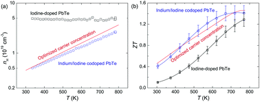
Thermoelectric properties are heavily dependent on the carrier concentration, and therefore the optimization of carrier concentration plays a central role in achieving high thermoelectric performance. The optimized carrier concentration is highly temperature-dependent and could even possibly vary within one order of magnitude in the temperature range of several hundreds of Kelvin. Practically, however, the traditional doping strategy will only lead to a constant carrier concentration, and thus the thermoelectric performance is only optimized within a limited temperature range. Here, we demonstrate that a temperature-dependent carrier concentration can be realized by simultaneously introducing shallow and deep defect levels. In this work, iodine (I) and indium (In) are co-doped in PbTe, where iodine acts as the shallow donor level that supplies sufficient electrons and indium builds up the localized half-filled deep defect state in the band gap. The indium deep defect state traps electrons at a lower temperature and the trapped electrons will be thermally activated back to the conduction band when the temperature rises. In this way, the carrier concentration can be engineered as temperature-dependent, which matches the theoretically predicted optimized carrier concentration over the whole temperature range. As a result, a room temperature ZT of ∼0.4 and a peak ZT of ∼1.4 at 773 K were obtained in the n-type In/I co-doped PbTe, leading to a record-high average ZT of ∼1.04 in the temperature range of 300 to 773 K. Importantly, since deep defect levels also exist in other materials, the strategy of deep defect level engineering should be widely applicable to a variety of materials for enhancing the thermoelectric performance across a broad temperature range.


 Please wait while we load your content...