
 Open Access Article
 This Open Access Article is licensed under a
 Creative Commons Attribution 3.0 Unported Licence
How small amounts of Ge modify the formation pathways and crystallization of kesterites
S.
Giraldo
a,
E.
Saucedo
 *a,
M.
Neuschitzer
a,
F.
Oliva
a,
M.
Placidi
a,
X.
Alcobé
b,
V.
Izquierdo-Roca
a,
S.
Kim
c,
H.
Tampo
c,
H.
Shibata
c,
A.
Pérez-Rodríguez
ad and
P.
Pistor
ae
*a,
M.
Neuschitzer
a,
F.
Oliva
a,
M.
Placidi
a,
X.
Alcobé
b,
V.
Izquierdo-Roca
a,
S.
Kim
c,
H.
Tampo
c,
H.
Shibata
c,
A.
Pérez-Rodríguez
ad and
P.
Pistor
ae
aCatalonia Institute for Energy Research (IREC), Jardins de les Dones de Negre 1, 08930 Sant Adrià de Besòs, Barcelona, Spain. E-mail: esaucedo@irec.cat; Tel: +34933562615
bCentres Científics i Tecnològics de la Universitat de Barcelona (CCiTUB), Lluís Solé i Sabarís 1-3, 08028 Barcelona, Spain
cResearch Center for Photovoltaics, National Institute of Advanced Industrial Science and Technology (AIST), 1-1-1 Umezono, Tsukuba, Ibaraki, 305-8568, Japan
dIN2UB, Departament d’Electrònica, Universitat de Barcelona, Martí i Franquès, 1-11, 08028, Barcelona, Spain
eInstitut für Physik, Martin-Luther-Universität Halle-Wittenberg, Halle, Germany
First published on 27th October 2017
Abstract
The inclusion of Ge into the synthesis of Cu2ZnSn(S,Se)4 absorbers for kesterite solar cells has been proven to be a very efficient way to boost the device efficiency in a couple of recent publications. This highlights the importance to elucidate the mechanisms by which Ge improves the kesterite solar cells properties to such a large extent. In this contribution, we first show how controlling the position and thickness of a very thin (10–15 nm) layer of Ge greatly influences the crystallization of kesterite thin films prepared in a sequential process. Typically, Cu2ZnSnSe4 (CZTSe) films form in a bi-layer structure with large grains in the upper region and small grains at the back. By introducing Ge nanolayers below our precursors, we observe that large CZTSe grains extending over the whole absorber thickness are formed. Additionally, we observe that Ge induces fundamental changes in the formation mechanism of the kesterite absorber. In a detailed analysis of the phase evolution with and without Ge, we combine the results of X-ray fluorescence, X-ray diffraction and Raman spectroscopy to demonstrate how the Ge influences the preferred reaction scheme during the selenization. We reveal that the presence of Ge causes a large change in the in-depth elemental distribution, induces a stabilizing Cu–Sn intermixing, and thus prevents drastic compositional fluctuations during the annealing process. This finally leads to a change from a tri-molecular towards, mainly, a bi-molecular CZTSe formation mechanism. Kesterite thin films with surprisingly large crystals of several microns in diameter can be fabricated using this approach. The results are related to the increase in device performance, where power conversion efficiencies of up to 11.8% were obtained. Finally, the consequences of the disclosed crystallization pathways and the extension to other chalcogenide technologies are discussed.
Broader contextDirect solar energy conversion into electricity (photovoltaic energy, PV) is probably the most relevant renewable energy source for the future sustainable development of humanity. In order to provide a significant share of the increasing global electricity demand in the short- to midterm, a mass deployment of PV installations in the TW regime will be needed. Ramping up the PV production to these large scales calls for the development of cheap PV technologies using earth abundant elements with low toxicity. Kesterite (Cu2ZnSn(S,Se)4-CZTS) thin film solar cells fulfil these criteria and are at the forefront of abundant inorganic materials for PV applications due to their intrinsic characteristics. Nevertheless, the performance of these device has so far been limited, mainly by their low open circuit voltage (VOC). The partial substitution of Sn by Ge has been shown as one of the most promising routes to boost the VOC, and has recently been demonstrated by several research groups around the world. Additionally, Ge is one of the most relevant candidates for the implementation of band-gap graded concepts in kesterites, similar to the grading strategies successfully implemented with In and Ga in high efficiency Cu(In,Ga)Se2 devices. However, the reasons behind the strong impact of relatively small quantities of Ge are still obscure. Herein we report our fundamental analysis of the impact of Ge on the phases formed during the reactive selenization, and the consequences these changes have on the absorber morphology and device performance. A change in the kesterite formation mechanism is observed from a tri-molecular pathway involving the binary selenides without Ge, to a bi-molecular one involving Cu–Sn alloys with Ge. This strongly modifies the main characteristics of the synthesized layer, above all the homogeneity, morphology and opto-electronic properties. Our findings explain how Ge avoids the formation of the segregated bi-layered structures traditionally observed in kesterite devices and provide hope that Ge might have beneficial effects on other chalcogenide thin film technologies, too. |
1. Introduction
Kesterite thin film photovoltaics (PV) based on Cu2ZnSn(S,Se)4 (CZTSSe) absorbers offer the same advantages as other large scale thin film production technologies such as CdTe or Cu(In,Ga)Se2 (CIGSe), being potentially capable of high throughput at large scale and enabling stable module performance, monolithic integration, aesthetic design and allowing the manufacturer to choose a suitable substrate (e.g. glass, flexible metal or polyimide foils). Kesterite PV is still much younger and has so far demonstrated a 12.6% record efficiency.1 Therefore, there is still a long way of technological engineering to go in order to catch up with its older chalcogenide cousins having already surpassed power conversion efficiencies of 20%.2The clear advantages of kesterites – cheap, earth-abundant and non-toxic constituents – make it a very attractive alternative absorber material, but these assets may only translate into industrial success if high efficiencies (towards 20%) can also be achieved. Main limitation for the performance in current kesterite solar cells is the relatively low open circuit voltage in comparison to other technologies.3–5 As the open circuit voltage of a given semiconductor is limited by its band gap, an adequate measure for comparing technologies with different band gaps is the voltage loss, defined as the difference between the band gap potential and the open circuit voltage. While for high efficiency CIGS and CdTe voltage losses of <0.4 V can be achieved, the best kesterite devices exhibit voltage losses of around 550–600 mV.5 Different origins for these voltage losses in kesterite solar cells have been proposed and are currently under discussion, among others strong potential fluctuations, band tailing, Cu/Zn disorder effects, interface recombination and/or the influence of secondary phases and compositional inhomogeneities.6–8
Recently, we have reported the great beneficial impact that nanometric Ge layers have on the performance and especially on the open circuit voltage of sequentially processed Cu2ZnSnSe4 (CZTSe) solar cells.9–11 In these cases, Ge thicknesses between 1–25 nm had been deposited on top of metallic Cu/Sn/Cu/Zn precursor stacks, which were then subjected to a reactive thermal treatment in order to selenize the precursors to CZTSe absorbers. A surprisingly large increase in the open circuit voltage up to 489 mV (compared to reference values, i.e. without Ge, around 400 mV) has been reported for an optimum Ge thickness of 10–15 nm, leading to an outstanding low voltage loss of only 0.56 V.11 The beneficial effect of incorporating small amounts of Ge has been reproduced afterwards in several other works.12,13 Kim et al.12 and Neuschitzer et al.14 have independently reported strongly enlarged grain sizes for Cu2Zn(Sn,Ge)Se4 absorbers that had been reannealed in a Ge containing atmosphere. However, the main lever of interaction underlying the “Ge boost” has not been clarified in detail. Several hypotheses have been formulated, as recapitulated in brief in the following:
(1) Surface modification: the initial idea behind the application of the Ge layers was to incorporate the Ge into the absorber and hence introduce a band gap grading towards the absorber surface. A graded absorber with higher band gap at the surface is expected to lower the interface recombination resulting in higher open circuit voltages. This effect can be observed in CIGS solar cells, where a gradient with increasing band gap towards the absorber surface is obtained through In/Ga or S/Se alloying.15,16 However, in ref. 9 we showed that for these small amounts of Ge no traceable amounts of Ge are incorporated into the absorber, no change in the absorber surface structure and no increase in the band gap is observed.
(2) Formation of a flux agent: the formation of Ge–Se phases that decompose incongruently into a GexSey (Se ∼85%) liquid, and volatile GeSe2 gas phase has been proposed explaining both, the low Ge incorporation in the CZTSe when small amounts of this element are used, and the observed improved crystallinity.9
(3) Interaction with Na: strong interaction between Ge and Na has been observed during the crystallization process, indicating that somehow Ge can help to control the Na content in kesterite bulk and surface. Additionally, this combines well with the idea that Ge is forming Ge–Se liquid phases at the surface during the annealing process that can act as crystallization flux and, at the same time, control the doping level of the absorber.10
(4) Improvement of transport charge properties: apparently Ge has a beneficial effect on the transport charge properties of kesterites, in particular increasing the carrier life-time, most probably interrelated to all the previously described improvements.17
Nevertheless, the reasons behind these improvements induced by Ge are still a matter of controversy. In this contribution, we investigate in depth the mechanisms underlying the Ge boost on kesterite solar cells and suggest an alternative mechanism based on the reaction scheme during selenization. For this purpose, kesterite absorbers are prepared in the standard sequential baseline process established at IREC, which is described in more detail in the experimental section. In this work, the amount and position (below and/or above the precursors) of deposited Ge is varied and correlated with the optoelectronic performance of the resulting devices. Differences in the reaction schemes during the selenization with and without Ge will be analyzed in detail with the help of energy-dispersive X-ray spectroscopy (EDX), X-ray fluorescence (XRF), X-ray diffraction (XRD) and Raman spectroscopy with multi-wavelength excitation for samples where the reactive annealing treatment had been interrupted at different points in time. It will be demonstrated that Ge has multiple effects on kesterites and that most of them are connected with the observation of a change in the synthesis mechanisms, together with the presence of Ge–Se liquid phases. Finally, we will show how this type of assisted crystallization can be extended in the future to other chalcogenide compounds with technological relevance.
2. Results
2.1. Effect on the phase formation and reaction schemes during selenization
Ge has shown to assist the crystallization of CZTSe, improving the morphology and electro-optical properties of this material. This is a recurrent observation in the literature, where several works have reported an increased grain growth for Ge containing absorbers.9,12,14 In spite of this, still a bilayer structure is frequently observed, with very big crystallites at the surface and smaller ones at the back, and the actual role of Ge in this system is still a matter of intense research.In this section, we will try to elucidate the role of Ge during the reactive thermal annealing process and how it assists the formation of large crystallites. The phases formed during the different steps of the reactive thermal annealing under selenium atmosphere will be compared for samples with and without Ge. For this purpose, ultrathin layers of Ge (10–25 nm) were deposited below the CTZ precursor (between the Mo back contact and precursors) and selenized in a specially designed “break-off” experiment. In order to better describe the design of the “break-off” experiment, the temperature profile of our standard process is depicted in Fig. 1. It consists of two stages: in the first stage, the pressure within the tubular furnace is set to 1 mbar (0 min, t0). The furnace is then heated at a rate of 20 K min−1. Once the set temperature of 400 °C is reached (18.5 min, t1), the temperature is hold for 30 min (48.5 min, t2). In the second stage, the pressure is increased to 1000 mbar through the inlet of Ar gas, and the temperature is increased to 550 °C (at 20 K min−1) (56 min, t3). This temperature is kept for 15 min (71 min, t4). After this, the system cools down naturally. At the times t1, t2, t3, t4 we have interrupted the reactive annealing process in order to investigate differences in the reaction schemes for the samples with/without Ge, and characterized the layers at different stages by SEM, EDX, XRD and Raman spectroscopy.
 | ||
| Fig. 1 Cross-sectional SEM micrographs of the CZTSe absorbers with different amounts of Ge (0 nm, 10 nm, 25 nm) deposited below the CTZ precursors (see Experimental section for a detailed nomenclature description). For these samples, the reactive annealing was interrupted after different times t1, t2, t3, t4, as marked in the temperature profile. | ||
In the same Fig. 1, cross-sectional micrographs of the different samples are depicted. In Fig. 2–4 samples with and without Ge are compared just after reaching the first temperature plateau at 400 °C (t1) using different characterization techniques. In Fig. 2 in-depth compositional maps of cross-sections obtained with EDX are displayed, while Fig. 3 and 4 show XRD diffractograms and Raman spectra, respectively. In the following, the results concerning the sample without Ge (0/CTZ/0) will be presented and then compared with the results obtained on the samples with Ge below the CTZ precursor (10/CTZ/0 and 25/CTZ/0). The nomenclature for the sample description is detailed in the experimental section at the end of this manuscript.
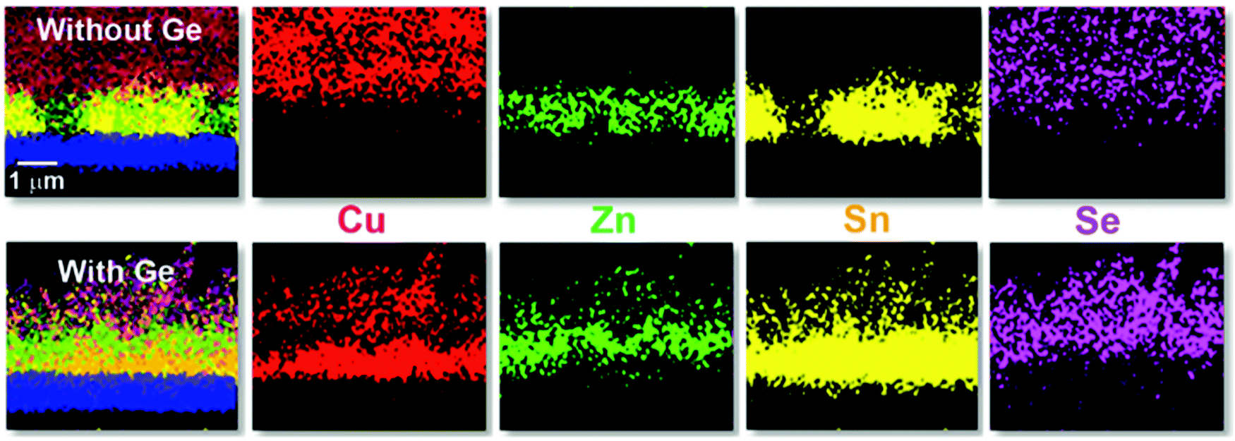 | ||
| Fig. 2 Cross-sectional elemental distribution of samples with and without Ge (25 nm below the CTZ precursor) after reaching the first temperature plateau (t1) determined by EDX (Cu, Zn, Sn and Se. Mo is depicted in blue just in the overlapped mapping for guidance). | ||
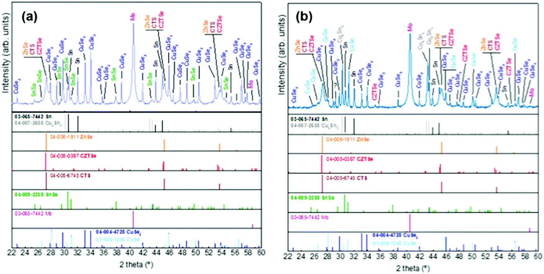 | ||
| Fig. 3 XRD diffractograms of samples without Ge at t1 (a) and with Ge (25 nm below the CTZ precursor) at t1 (b). | ||
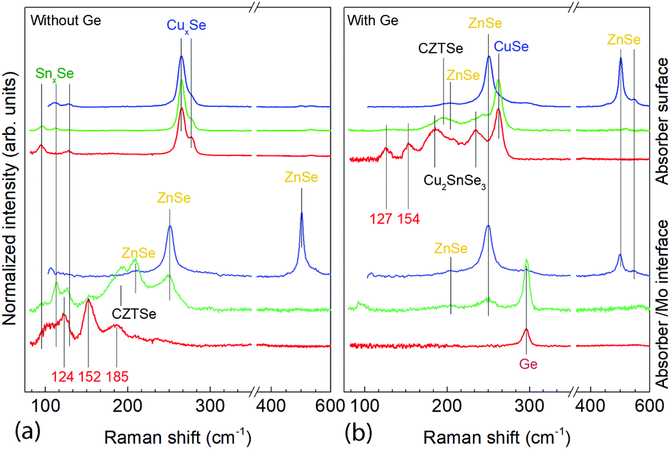 | ||
| Fig. 4 Raman spectra using three different excitation wavelengths at the absorber surface and absorber back side for the sample without Ge at t1 and with Ge (25 nm below the CTZ precursor) at t1. Red: 633 nm, green: 532 nm and blue: 488 nm. | ||
At t1 we expect that the simplest compounds (binary or ternary) will be formed that will then react during the t1–t2 dwell time in order to form the quaternary kesterite. In this sense, it is very relevant to identify which phases actually form at t1 since it will bring first-hand information about the reaction pathway. In Fig. 3a, an XRD diffractogram of the sample without Ge (0/CTZ/0) at t1 is shown. The XRD analysis provides evidence that elemental Sn is the only metallic phase, suggesting that Cu and Zn have already reacted completely with Se. In fact, CuSe2 is clearly identified in the XRD diffractogram together with some SnSe. Additionally, diffraction peaks are observed that can correspond either to ZnSe, Cu2SnSe3 and/or Cu2ZnSnSe4, confirming that one or more of these phases are present. However, characteristic further peaks corresponding to the lowered symmetry of the tetragonal phase of CZTSe are absent, excluding the presence of significant amounts of crystalline CZTSe. In order to support the XRD analysis, Raman spectra measured with different excitation wavelengths (633 nm, 532 nm, 488 nm) at the surface of this sample and (after lift-off) at the back side of the absorber are shown in Fig. 4a. At the surface, CuxSe is clearly detected with all three excitation wavelengths,22 in agreement with the EDX and XRD analysis. At the back side, ZnSe is observed when using 488 nm excitation23 together with Sn–Se phases,24 and a very weak and broad band that is tentatively attributed to amorphous CZTSe. In any case, no evidences of Cu–Sn–Se phases are present, in agreement with the in-depth physical separation of Cu and Sn observed by EDX.
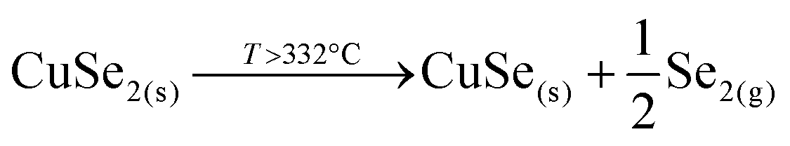
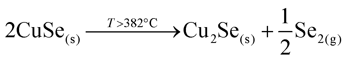
This strongly suggests that the kesterite formation proceeds via the reaction of binary compounds (Cu, Zn and Sn selenides) as has been reported for the sulphide kesterite compound Cu2ZnSnS4.21 The presence of the CuSe2 phase indicates that the reaction is in fact much more complex than previously believed. CuSe2 is the phase with the lowest formation energy in the complex Cu–Se system.25 In our annealing conditions, a high Se overpressure builds up at the very beginning. These two conditions together explain the formation of CuSe2. Nevertheless, above a temperature of 332 °C this phase decomposes into CuSe, and then into Cu2Se above 382 °C25, following the reactions below:
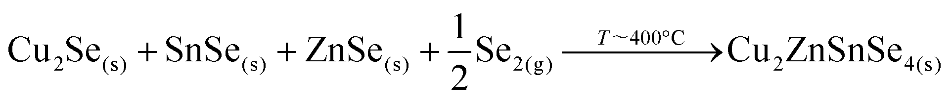
Then, Cu2Se is expected to react with SnSe and ZnSe to form the kesterite through the following reaction:
This reaction mechanism is firmly supported by the EDX, XRD and Raman analysis presented up to now. It implies another important point: the presence of SnSe at the beginning of the process, as is clearly evidenced by both the XRD and Raman analysis. The volatility of SnSe bears the high risk of Sn-loss during the reaction, a fact that is corroborated by a look at the analysis of the compositional ratios by X-ray fluorescence (XRF): while the initial precursor has a C/ZT of 0.76 and Z/T = 1.20, at t1 these have increased to C/ZT = 0.99 and Z/T = 1.68 as a result of substantial Sn loss. Therefore, the overall composition of the reference layer without Ge at t1 is in fact notably poorer in Sn than the initial precursors as a result of the uncontrolled Sn-loss.
The presence of almost all the Cu at the front might be the origin of the large grains formed at the surface of the absorbers, where the kesterite is growing under Cu-rich conditions from CuxSe. On the contrary, the low Cu concentration at the back (Cu-poor conditions) prevents the formation of large grains, as is commonly observed. The morphology of these layers, in particular the bi-layered structure and the formation of voids at the back side can therefore be explained as a result of this tri-molecular reaction mechanism (with three binary selenide compounds) and the involved Cu-out diffusion and segregation of Cu and Sn/Zn selenides. Intriguingly, Thersleff et al. have reported in a detailed analysis of a similar bi-layered structure that the back region in the final CZTSe made up by small grains is still Cu-poorer than the region with larger grains at the surface, supporting our model of differential grain growth at back and front.26 In the next sub-section we will show how this story drastically changes once Ge is introduced below the CTZ precursor.
One of the first consequences is the drastic reduction of Sn-loss in this first stage (t1). XRF measurements reveal that the C/ZT and Z/T ratios remain almost the same after t1 (0.78 and 1.27, respectively) as compared to the initial precursor composition (0.76 and 1.20) for the samples with Ge. This means that practically no Sn is lost to the annealing atmosphere, again in contrast to the Ge-free sample.
It is important to remark that the presence of Ge seems to minimize or even avoid two important issues affecting the morphology of CZTSe layers: the fast Cu-out diffusion and the uncontrolled Sn-loss. This notably also impacts on the final absorber morphology as is clearly observed in Fig. 1 for the samples with Ge at t4. For the sample 10/CTZ/0, already at t3 a nice morphology is observed, while at t4 (end of the annealing process), huge grains extending over the whole absorber thickness are obtained (even substantially wider than high), and with no observable voids or imperfections at the back interface. In consequence, we claim that the Ge containing samples are capable of holding the Sn within the precursors at the beginning of the selenization and avoid/minimize the fast Cu-out diffusion and Cu/Sn segregation observed for Ge-free samples. This is crucial for the improved selenization reaction, as will be discussed in Section 3.
The further characterization by XRD and Raman spectroscopy of the Ge-containing samples completely support this picture. As is observed in Fig. 3b, the XRD pattern of the sample containing Ge at t1 is very different to the sample without Ge. As stated earlier, two metallic phases are clearly detected: Sn and Cu6Sn5, confirming that somehow the presence of Ge at the back stabilizes the Cu–Sn alloys. Additionally, the presence of CuSe and CuSe2 are confirmed, and once again the diffraction peaks corresponding to CZTSe and/or Cu2SnSe3 and/or ZnSe. However, in this case the low intensity diffraction peaks corresponding to the tetragonal phases can clearly be identified, proving an early formation of the quaternary kesterite and/or ternary Cu2SnSe3 tetragonal phase.
Further differences are revealed by the Raman analysis (Fig. 4b). As expected, ZnSe is detected at both, the back and front side of the layer. On the other hand, Cu–Se is also detected at the front together with evidence for the formation of a Cu2SnSe3 phase, and a small quantity of a nanocrystalline or amorphous kesterite phase. But most relevant, the characteristic peaks of the Sn–Se phases are absent. This means that the pathway for kesterite formation mechanism has now changed and seems not occur via the binary Sn, Cu and Zn selenide phases as before.
The confirmed presence of Cu6Sn5 and Sn metallic phases suggests that the first step in this case is related to the formation and maybe already decomposition of bronze at temperatures close to 400 °C through:27

Then, the Cu3Sn phase can immediately react with Se2(g) to form:

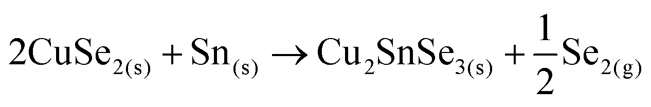
After that, the CuSe2 phase can follow a similar pathway to the proposed above for the sample without Ge as a competitive mechanism to form kesterite, or react with the free elemental Sn as follows:
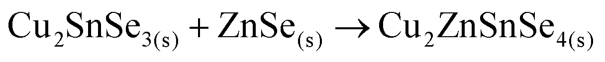
Finally, the ternary Cu–Sn–Se compound can react with ZnSe to form the CZTSe kesterite:
This implies the change from a tri-molecular reaction pathway as observed for the samples without Ge, towards a bimolecular one when using Ge. Additionally, this pathway does not involve the formation of a Sn–Se phase in any step, in line with the XRF, XRD and Raman spectroscopy results.
To summarize, the presence of very small amounts of Ge drastically modifies the reaction pathway in which the kesterite is formed. This notably impacts on the absorber morphology, the Sn loss and consequently on the devices properties, as will be further demonstrated in the following sections. It is worth to mention that we cannot rule out that Ge is assisting the crystallization also through the formation of Ge–Se liquid phases as has been reported elsewhere.9 Nevertheless, this alternative explanation is also not necessarily in contradiction with the mechanisms proposed in this paper.
2.2. Effect on the solar cell devices
Now, the question is what happens when these improved layers are implemented as photovoltaic absorbers. In order to analyze this question, series with CZTSe absorbers with different amounts of Ge deposited on top and below the CTZ precursors were prepared. Fig. 5 shows the evolution of the average solar cell parameters of a series were varying amounts of Ge (0–25 nm) were deposited below the metallic precursors, in addition to a 5 nm Ge layer on top.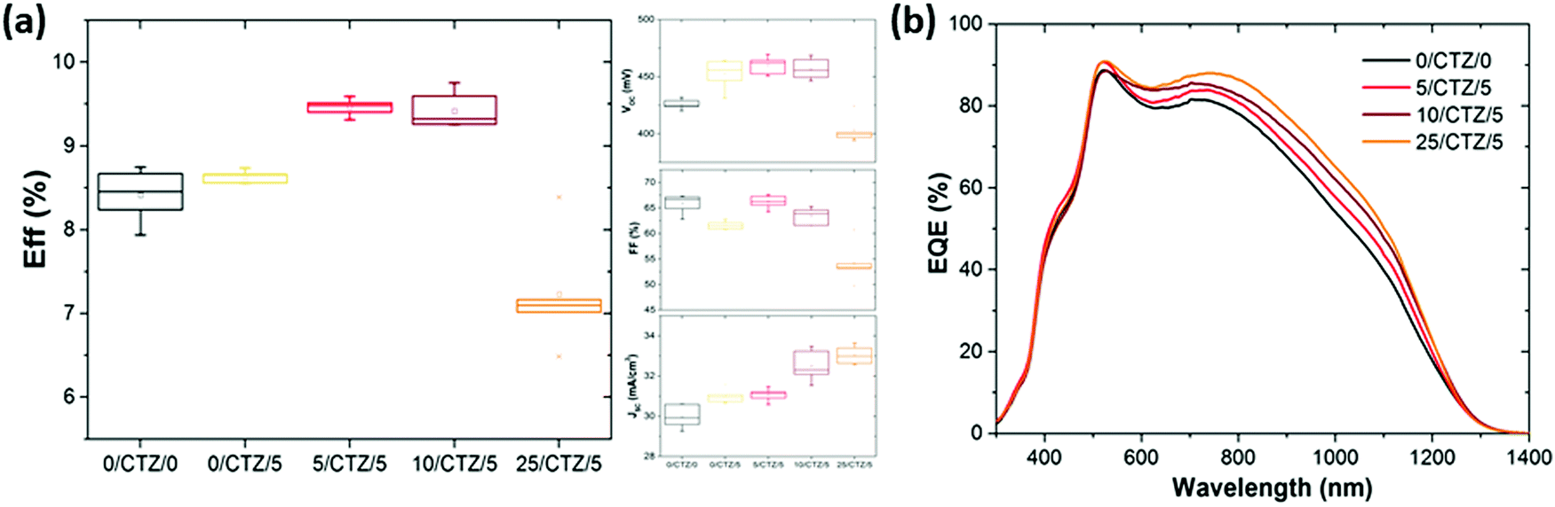 | ||
| Fig. 5 Effect of depositing a Ge layer of varying thickness prior to the metallic precursor deposition on (a) the solar cells parameters, and (b) the external quantum efficiency. All samples had additionally 5 nm Ge layer on top of the precursors, except for the reference sample (without Ge). The samples nomenclature is detailed in the Experimental section. | ||
The average efficiency (6 cells) increases from 8.6% to 9.5% if a thin (5 nm) Ge layer is deposited below the CTZ in addition to the top 5 nm Ge layer. If the thickness of the bottom layer is increased to 10 nm, the efficiency remains high (9.4%). This efficiency increase is mainly achieved by an enhanced short circuit current density, while the open circuit voltage remains at the same high value for these three samples, at 450–460 mV. The inset of Fig. 5 shows the external quantum efficiency of devices with different amounts of Ge below the CTZ, and elucidates that the origin of the JSC improvement is found in the longer wavelength range, related to collection of charge carriers from regions deep within the absorber.
We associate these improvements to a better charge carrier collection due to the better crystallinity as shown in the micrographs in Fig. 6. These micrographs again confirm the substantially improved morphology, especially towards the back contact, for the samples where the Ge was deposited between the back contact and precursors. Similar to the case of Ge layers deposited on top, a too thick Ge layer (25 nm) below the CTZ results in severe losses in fill factor (FF) and open circuit voltage (VOC).
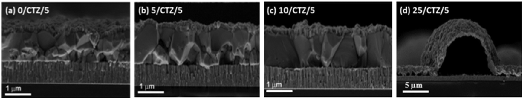 | ||
| Fig. 6 Cross-sectional SEM micrographs of the completed CZTSe solar cells with different amounts of Ge deposited below the metallic Cu/Sn/Cu/Zn precursor stack: (a) 0 nm Ge below, (b) 5 nm Ge below, (c) 10 nm Ge below, (d) 25 nm Ge below. All precursors had deposited a 5 nm Ge layer on top. | ||
For this sample, the absorber layer is forming “dome”-like features all over the substrate. We interpret these as bubbles that form during the absorber formation by uncontrolled evaporation of volatile Ge–Se species. A close examination of Fig. 1 reveals similar features for the sample with 25 nm Ge below the precursors presented there, however less pronounced.
In our previous work, where Ge was only deposited on top of the precursors, we found an optimal Ge thickness of 5–15 nm.11 Varying the Ge thickness above and below the CTZ precursors, we find the optimum for the global (sum of above and below) Ge thickness to be the same: 10–15 nm. The outcomes of the Ge variations above and below the precursors are summarized in Table 1 and Fig. 5, and clearly show:
| Sample | Ge layer (nm) | Eff. (%) | V OC (mV) | J SC (mA cm−2) | FF (%) | |
|---|---|---|---|---|---|---|
| Below | On top | |||||
| 0/CTZ/0 | — | — | 8.4 ± 0.3 | 426 ± 5 | 30.0 ± 0.6 | 65.9 ± 1.8 |
| 0/CTZ/5 | — | 5 | 8.6 ± 0.1 | 453 ± 13 | 31.0 ± 0.4 | 61.6 ± 0.8 |
| 0/CTZ/10 | — | 10 | 9.3 ± 0.1 | 455 ± 12 | 30.7 ± 0.6 | 66.6 ± 1.3 |
| 5/CTZ/5 | 5 | 5 | 9.5 ± 0.1 | 460 ± 8 | 31.1 ± 0.4 | 66.2 ± 1.3 |
| 10/CTZ/0 | 10 | — | 9.6 ± 0.2 | 466 ± 7 | 32.3 ± 0.7 | 64.1 ± 0.8 |
| 5/CTZ/10 | 5 | 10 | 9.4 ± 0.2 | 461 ± 7 | 30.9 ± 0.3 | 65.9 ± 1.2 |
| 10/CTZ/5 | 10 | 5 | 9.4 ± 0.3 | 457 ± 9 | 32.5 ± 0.8 | 63.5 ± 1.6 |
(1) All devices with an overall Ge thickness of 10–15 nm reproducibly lead to an improved VOC of 450–470 mV and efficiencies above 9.3%, while the reference values (i.e. without Ge) remain below 430 mV and below 9% respectively.
(2) Adding 25 nm Ge or more below or above the CTZ annihilates the beneficial effect of Ge and severely degrades the device performance.
(3) A slight increase in the short circuit current density is consistently observed for devices with Ge, up to 32.3–32.5 mA cm−2 for samples with small amounts of Ge introduced below the CTZ, while the reference values (i.e. without Ge) remain below 31.0 mA cm−2.
We therefore conclude that the positive effect of the Ge on the VOC (the VOC boost) is achieved for Ge thicknesses of 5–15 nm regardless of the position of the Ge nanolayer (below and/or above the CTZ precursor). This implies that the beneficial effect of the Ge is not limited to some surface modifications as previously suggested, but rather affects the whole bulk of the absorber. The best solar cell of this series reached an efficiency of 9.9% (VOC of 453 mV, FF of 67.1%, JSC of 32.5 mA cm−2), with 10 nm Ge below and 5 nm on top of the precursor (no anti-reflective coating applied).
3. Discussion
In a detailed high-resolution transmission electron microscopy (HR TEM) analysis it has been previously shown how the addition of 10 nm Ge on top of the precursors leads to a bi-layered absorber morphology and two distinct types of grain boundaries.26 These were denominated “straight” and potentially malign “meandering” grain boundaries. The bi-layer structure consisted of large grains and vertical “straight” grain boundaries near the surface, separated from the lower part towards the back side of the absorber, which was characterized by voids, horizontal “meandering” grain boundaries and a slightly lower (1.40 ± 0.03) Cu/Zn ratio than the top part (1.49 ± 0.03). Large grains stretching over the complete absorber thickness can be observed for the sample where the 10 nm Ge have been deposited below the precursor. In this sample, the increased crystallization enabled to completely remove the “meandering” horizontal grain boundaries from the sample, with an absorber built up by large grains and straight, vertical grain boundaries. Huge grains with lateral extensions exceeding 4 microns were found. As a matter fact, we have never observed or found evidence for comparable grain sizes and morphologies in prior work. The absence of the meandering grain boundaries in this type of samples might be an explanation for the improved charge collection, as resistive barriers and recombination centers at the bottom part of the absorber are removed.Based on the presented results, we suggest a fundamental difference in the reaction schemes for the samples containing Ge and the Ge-free ones. Scheme 2 depicts a schematic representation of the proposed model. For the Ge-free reference sample, Cu out-diffuses rapidly to the surface and forms Cu–Se as a dense, compact film on top of the Sn–Zn precursor. Se diffuses into the film and forms a porous region consisting of Sn–Se and Zn–Se. The reaction occurs predominantly via the formation of the binaries Zn–Se, Sn–Se and Cu–Se. As the Sn–Se phases have very high vapor pressures, a substantial loss of Sn occurs in the initial stage of the process. The loss of Sn–Se is a commonly observed issue in the synthesis of kesterites,28 and in fact is the reason for incorporating an additional amount of Sn within the graphite box during processing. Thus, the evaporation of this Sn during the further evolution of the process causes a high Sn–Se partial pressure in the graphite box, which in turn leads to a re-incorporation of Sn into the absorber at later stages.29 This self-regulation of the Sn content of the absorber is a well-known feature of the regular sequential processing and has been repeatedly observed. It is also reported in ref. 30 for sulphur-based kesterites. The Sn content, or the Cu/Sn ratio of the samples has been found to be crucial for the crystal growth and absorber quality in the past. A lower Cu/Sn ratio significantly enhances the crystallization and formation of large grains as is reported for example in ref. 31. Furthermore, Sugimoto et al. have shown that a lower Cu/Sn ratio in the absorbers is linked to increased charge carrier lifetimes and open circuit voltages.32
On the other hand, we could now demonstrate that the incorporation of Ge into the CTZ precursor prevents the Sn loss to some extent, firstly because Sn remains mainly fixed into a Cu–Sn–Se ternary phase, and additionally because a quaternary kesterite phase is formed much earlier. Here, during the heating, a Cu–Sn alloy is formed near the bottom region, close to the back contact. Se is diffusing into the precursor forming Zn–Se nano-crystals and large Cu–Se platelets at the surface, which also contain some Sn. In this case, the formation of Cu–Sn–Se ternary and Cu–Zn–Sn–Se phases already during the very first stages of the process effectively limits the Sn loss. There are two possible mechanisms how the Ge may assist the formation of the ternary phases and enlarged crystals. In the first model, small amounts of Ge incorporated into the Cu/Cu–Se might substantially increase the solubility of Sn within these phases and in consequence facilitate the crystallization and the formation of Cu–Sn–Se ternary phases. A similar effect is found for In and CZTSe: adding small amounts of In into the kesterite structure greatly increases the solubility of Zn in the kesterite phase.33 This is e.g. used to prevent the segregation of ZnSe secondary phases during the absorber synthesis. A second plausible mechanism is the formation of a liquid Ge–Se phase that acts as a flux agent for the formation of the Cu–Sn–Se and Cu–Zn–Sn–Se phases, similar to the effect that Cu–Se has on the growth of chalcopyrite Cu(In,Ga)Se2.34 In chalcopyrite synthesis, a Cu-rich growth phase leads to a substantial improvement of the grain size and absorber quality. The generally accepted model for this growth mechanism implies the formation of Cu–Se phases on the surface of the absorber once the Cu/(In + Ga) ratio surpasses 1 (Cu-rich growth phase). Then, the Cu–Se phase acts as a flux agent for the growth of large chalcopyrite crystals with a low defect density. The small amount of Ge present during the synthesis in our case makes its detection and location rather difficult, which in turn, at this moment, represents an obstacle for the distinction whether the Ge is incorporated into the Cu–Sn–Se phases or is present in a separate Ge–Se liquid phase. Further investigations to clarify these details are under way.
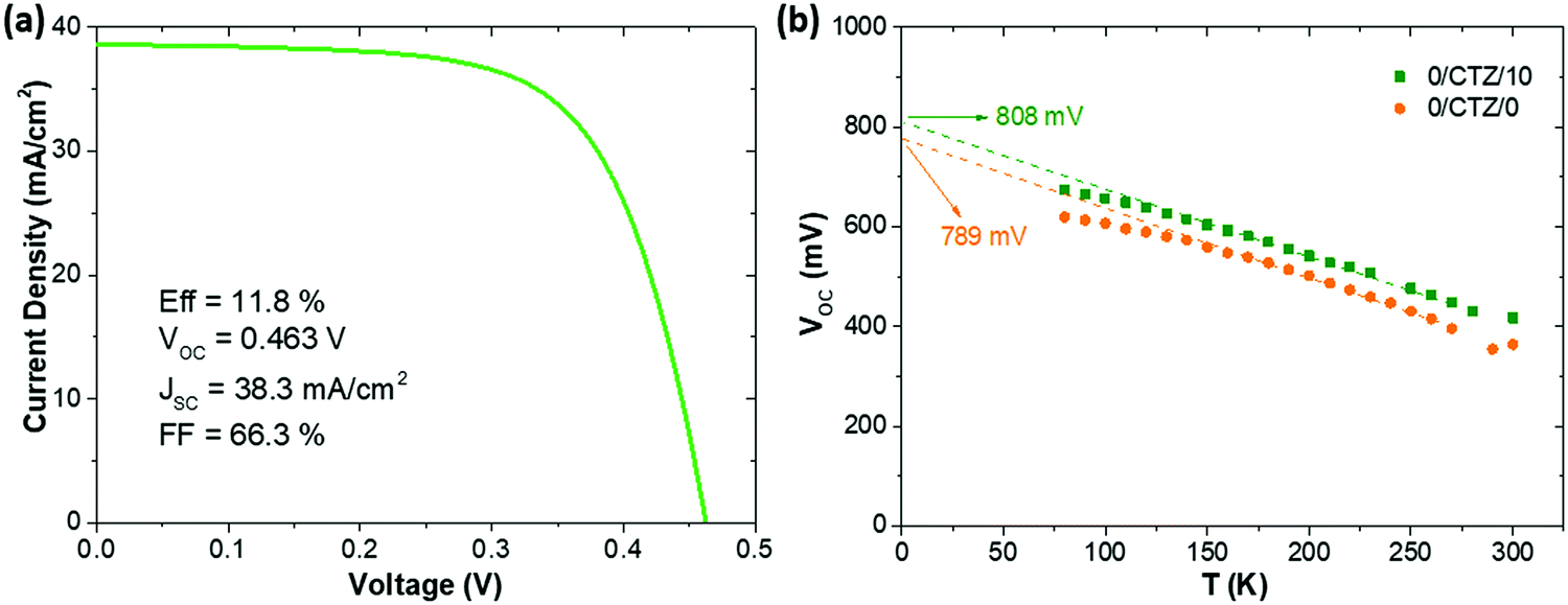
Ultimately, after optimizing all the processes presented here and implementing MgF2 anti-reflective coating as well as Ag grids to a CZTSe (+12.5 nm Ge) device, we achieved a record solar cell with an efficiency (illuminated area, not including the contact grid) of 11.8% with a VOC of 463 mV, FF of 66.3% and JSC of 38.3 mA cm−2. Referring to the total area (cell area of 0.522 cm2, including the contact grid) this measurement corresponds to an efficiency of 11.0% and a JSC of 36.0 mA cm−2. The JV-curve corresponding to this device is shown in Fig. 7a. A comparison with literature data for the best devices with pure selenide-based kesterite absorbers shows that this is among the highest efficiencies reported for this type of absorber. The best efficiency so far has been reported by IBM, with a remarkably lower VOC (423 mV), and higher JSC (40.6 mA cm−2), but resulting in a similar efficiency (total area efficiency of 11.6%) and FF (67.3%) for a slightly smaller device area (0.43 cm2).35 Other high performance devices reported by IMEC36 and Nankai University37 exhibit remarkably lower VOC (between 390–420 mV) and efficiencies (both 10.4%). Devices reported previously by IREC show systematically higher VOC values (typically between 460–490 mV).9,11,18 This emphasizes the impact that Ge has on the improved voltage deficit in kesterite solar cells.
 | ||
| Fig. 7 (a) J–V curve corresponding to the best solar cell obtained in this work. (b) VOCvs. T plot of a reference sample without Ge and a sample with 10 nm of Ge deposited on top of the CTZ precursors. | ||
Fig. 7b shows a VOCvs. temperature plot of two representative cells, one without Ge and one with 10 nm of Ge deposited on top of the precursors prior to selenization. The VOC of our CZTSe devices generally does not extrapolate at 0 K to the band gap energy (roughly 1.05 eV), but rather 150–220 mV below it (780–820 mV). As Fig. 7 shows, this is not significantly changed upon the addition of Ge. Both devices show a fairly linear increase of the VOC with decreasing temperature, as is expected for one dominant recombination mechanism which is thermally activated. The activation energy Ea of the recombination can in this case be extracted by an extrapolation of the VOC to 0 K (VOC (0 K)). For a dominant recombination in the bulk, the activation energy is generally expected to coincide with the band gap. As can be seen, the VOC of both samples evolve very similar, with the device without Ge extrapolating to 789 mV, and the sample with Ge to 808 mV. The case of VOC (0 K) < EG is generally associated with interface recombination, where a lowered interface band gap (e.g. due to band misalignments) determines the activation energy of the dominant recombination path.38 However, for CZTSe the interface band gap is reported not to be significantly lowered,39 in contrast to CZTS, and other origins for a reduced Ea are also possible, e.g. high densities of tail states within the band gap, recombination via grain boundaries/secondary phase inclusions with reduced band gap or fermi level pinning.38 The preliminary results presented here do not allow a clear location of the dominant recombination mechanism yet. However, the rather similar behaviour of the VOC (T) does not indicate a fundamental change in the recombination mechanism (e.g. from interface to bulk). We therefore do not expect the observed improvement to be located at the absorber/buffer interface, but rather in the absorber bulk, e.g. due to an increased charge carrier lifetime.
For a deeper understanding of the effect of Ge on the intrinsic electronic properties of the absorbers and corresponding solar cells, a more complete characterization of a broad set of devices is required, together with an analysis of possible changes in the absorber surface and the absorber/buffer interface properties. This work is currently under way and will be published elsewhere.
Finally, an interesting question remains. Is the beneficial effect of Ge restricted to the synthesis of kesterites, or can it be applied to other chalcogenides used for photovoltaics? In order to test the impact of Ge on chalcopyrites, CuInSe2 (CISe) was synthesized without and with a 25 nm Ge nanolayer below the precursor by a sequential process similar to the one used for kesterite absorbers (sputtering of Cu and In metallic stacks, followed by selenization in a graphite box). Fig. 8 shows the cross-sectional and surface SEM images of the resulting CISe layers. Surprisingly, the application of nanometric Ge layers also leads to significantly enlarged grains in this case. While we cannot answer the question of the global impact of Ge on chalcopyrites satisfactorily at the moment, our preliminary results at least strongly encourage a further investigation of the impact of Ge on the growth, crystallization, morphology and devices for other chalcogenides.
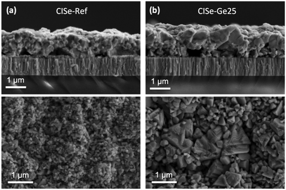 | ||
| Fig. 8 SEM micrographs of CISe layers without Ge (a) and with 25 nm Ge (b), selenized at 450 °C for 30 min at 1 mbar Ar pressure. | ||
4. Conclusions
Here we present a new concept for obtaining high quality CZTSe layers, by introducing an extremely thin Ge nanolayer at the back region, studying the impact and the origin of the recurrently observed positive effect of Ge in the kesterite system. We observe that the presence of Ge strongly affects the in-depth elemental distribution, delaying and minimizing the fast Cu-out diffusion and the formation of Sn–Se volatile species, and consequently avoiding Sn losses to a large extent. This allows modifying the reaction pathways of CZTSe from a tri-molecular mechanism for the layers without Ge, towards a mainly bi-molecular one for the samples containing Ge. The immediate effect is the large improvement of the CZTSe morphology, where very well crystallized layers with grains extending over the whole thickness are easily obtained. The main role of Ge seems to be related to the stabilization of Cu–Sn phases, impacting in the elemental in-depth distribution and ultimately in the reaction pathways of the kesterite. Through the optimization of the quantity of Ge together with the location of this element, we succeed to achieve a device that can be considered almost pure Cu2ZnSnSe4 and with 11.8% conversion efficiency.5. Experimental
Kesterite absorbers were prepared on soda-lime glass substrates with an optimized tri-layer Mo back contact of approximately 800 nm. Details on the Mo back contact optimization can be found in ref. 18. The absorber synthesis is schematized in Scheme 1 and consisted of a sputter-deposition of metallic Cu(4 nm)/Sn(245 nm)/Cu(182 nm)/Zn(168 nm) precursors. These precursors usually yield suitable kesterite absorbers after selenization with Cu/(Zn + Sn) (C/ZT) ratios of 0.75–0.77 and Zn/Sn (Z/T) of 1.20–1.22. In the current variations, Ge layers of thicknesses between 5–25 nm were thermally evaporated onto the substrates before and/or after the metallic precursors, resulting in stacks were the Ge layers were situated below and/or above the metallic precursors. In the following, samples will be denominated by the thickness (in nm) and position of the deposited Ge layer, for example: CTZ/5 stands for 5 nm Ge on top of the metallic precursors, 10/CTZ corresponds to 10 nm Ge below the precursors, 25/CTZ/5 means 25 nm Ge below and 5 nm Ge on top and so on.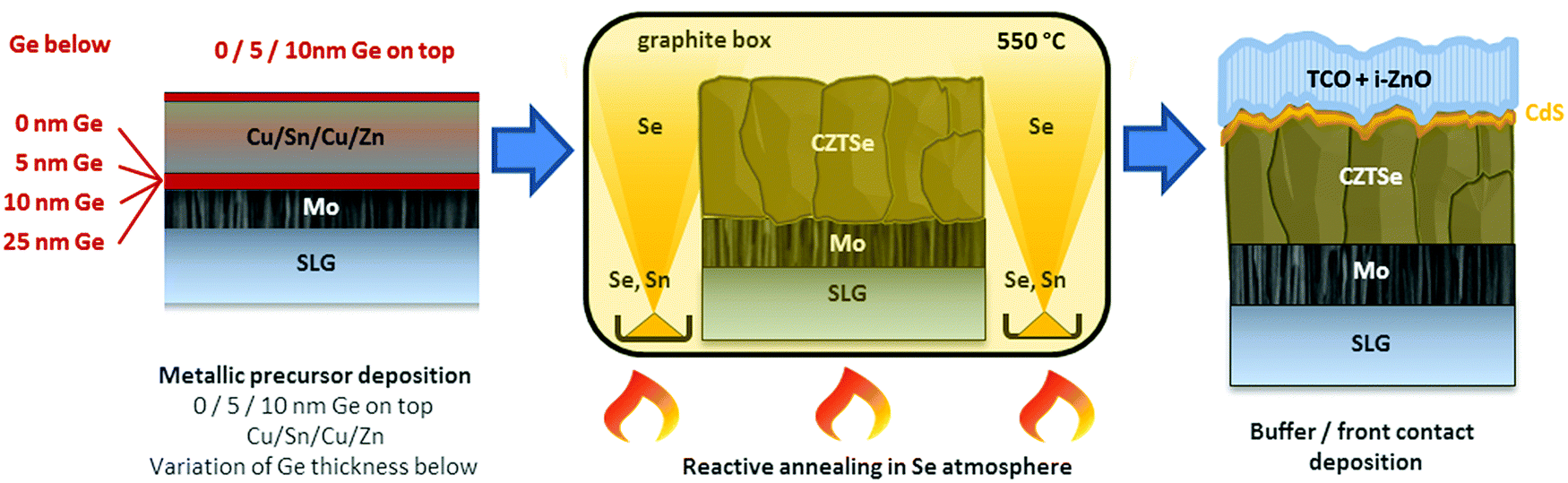 | ||
| Scheme 1 Sketch of the CZTSe absorber preparation: (1) deposition of Cu/Sn/Cu/Zn metallic precursors by magnetron sputtering. Nanometric Ge layers are evaporated onto the substrate before and/or after the precursors. (2) Reactive annealing with elemental Se (and Sn) in a semi-closed graphite box. (3) Completed CZTSe solar cell structure. | ||
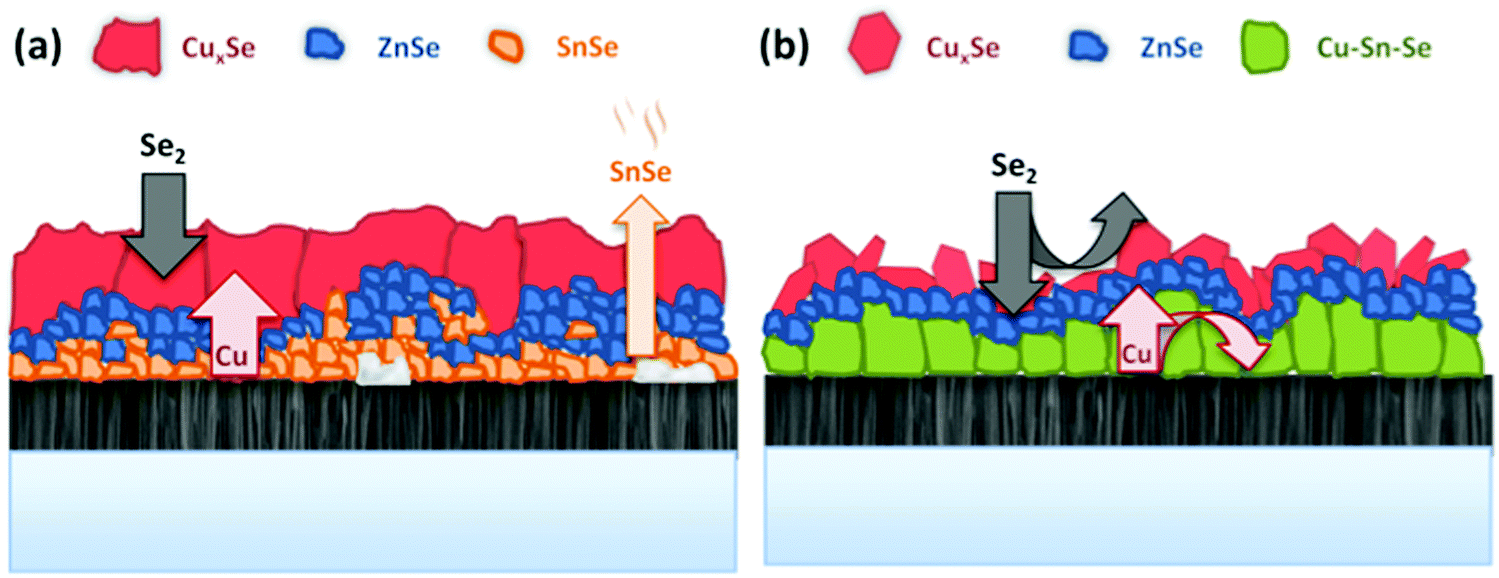 | ||
| Scheme 2 Schematic sketches of the different intermediate steps and reaction mechanisms involved in the formation of CZTSe during the selenization of metallic Cu–Zn–Sn precursors: (a) reference sample without Ge, and (b) Ge-containing sample. | ||
The metallic CTZ precursors (with and without Ge) where then placed in a graphite box together with 100 mg of Se and 5 mg of Sn for the reactive thermal annealing. The reactive thermal annealing was realized in a tubular furnace and Ar atmosphere by a first heating step at 400 °C for 30 min (1 mbar) and a second step at 550 °C for 15 min (1000 mbar). The temperature profile of the reactive thermal annealing is depicted in Fig. 1. More details on the baseline absorber synthesis can be found in ref. 9. For the analysis of the reaction pathways, the annealing process was stopped at different relevant points as schematized in the Fig. 1.
Following the baseline routine established at IREC, the samples were then subjected to a wet-chemical etching/passivation step in (NH4)2S (22% v/v, for 2 min),19 a chemical bath for the deposition of CdS20 before the devices were finished by sputter-depositing an i-ZnO/ITO window layer. For IV and EQE-characterization, the devices were mechanically scribed into cells with a size of 3 mm × 3 mm and measured under simulated AM1.5 illumination from an AAA solar simulator (Abet Technologies). With the best samples, devices of 0.522 cm2 in area and including MgF2 anti-reflective coating and Ag metallic grids were fabricated. Finished devices were post-deposition annealed in air on a hot plate for 15 min at a temperature of 250 °C.
X-ray fluorescence (XRF, Fischerscope XVD) was used to determine the overall composition and thickness of the different precursor and absorber layers. Scanning electron microscopy (SEM) images were obtained with a ZEISS Series Auriga microscope using 5 kV accelerating voltage. Energy dispersive X-ray spectroscopy (EDX) analysis was performed with a 20 kV acceleration voltage using an INCA 250 series EDS detector from Oxford Instruments on the cross-sections of selected samples, with and without Ge. X-ray diffraction (XRD) was carried out using a PANalytical X'Pert PRO MPD Alpha1 powder diffractometer in Bragg–Brentano θ/2θ geometry, from 4 to 145° with step size of 0.017° and integration time of 200 s per step, using Cu Kα1 radiation (λ1/41.5406 Å). Raman spectroscopy was performed with an iHR320 Horiba-Jobin Yvon spectrometer coupled to a Raman probe developed at IREC and a CCD detector, using three different excitation wavelengths (red: 633 nm, green: 532 nm, and blue: 488 nm).
Conflicts of interest
There are no conflicts to declare.Acknowledgements
This research was supported by the H2020 Programme under the project STARCELL (H2020-NMBP-03-2016-720907), by MINECO (Ministerio de Economía y Competitividad de España) under the NASCENT project (ENE2014-56237-C4-1-R), by the European Regional Development Funds (ERDF, FEDER Programa Competitivitat de Catalunya 2007–2013) and CERCA Programme/Generalitat de Catalunya. Authors from IREC and the University of Barcelona belong to the M-2E (Electronic Materials for Energy) Consolidated Research Group and the XaRMAE Network of Excellence on Materials for Energy of the “Generalitat de Catalunya”. S. G. thanks the Government of Spain for the FPI fellowship (BES-2014-068533). P. P. thanks the European Union for a Marie Curie Individual Fellowship (“JUMPKEST”, FP7-PEOPLE-2013-IEF- 625840) and his wife for her continuous support.References
- W. Wang, M. T. Winkler, O. Gunawan, T. Gokmen, T. K. Todorov, Y. Zhu and D. B. Mitzi, Device Characteristics of CZTSSe Thin-Film Solar Cells with 12.6% Efficiency, Adv. Energy Mater., 2014, 4(7), 1301465 CrossRef.
- P. Jackson, R. Wuerz, D. Hariskos, E. Lotter, W. Witte and M. Powalla, Effects of Heavy Alkali Elements in Cu(In,Ga)Se2 Solar Cells with Efficiencies up to 22.6%, Phys. Status Solidi RRL, 2016, 10(8), 583–586 CrossRef CAS.
- K. Kaur, N. Kumar, M. Kumar, Q. Guo, L. K. Johnson, R. S. Mclean, I. Malajovich, K. R. Choudhury, P. Scardi and A. Mittiga, Strategic Review of Interface Carrier Recombination in Earth Abundant Cu–Zn–Sn–S–Se Solar Cells: Current Challenges and Future Prospects, J. Mater. Chem. A, 2017, 5(7), 3069–3090 CAS.
- A. Polman, M. Knight, E. C. Garnett, B. Ehrler and W. C. Sinke, Photovoltaic Materials: Present Efficiencies and Future Challenges, Science, 2016, 352, 6283 CrossRef PubMed.
- J. Kim and B. Shin, Strategies to Reduce the Open-Circuit Voltage Deficit in Cu2ZnSn(S,Se)4 Thin Film Solar Cells, Electron. Mater. Lett., 2017, 1–20 Search PubMed.
- T. Gokmen, O. Gunawan, T. K. Todorov and D. B. Mitzi, Band Tailing and Efficiency Limitation in Kesterite Solar Cells, Appl. Phys. Lett., 2013, 103(10), 103506 CrossRef.
- S. Bourdais, C. Choné, B. Delatouche, A. Jacob, G. Larramona, C. Moisan, A. Lafond, F. Donatini, G. Rey, S. Siebentritt, A. Walsh and G. Dennler, Is the Cu/Zn Disorder the Main Culprit for the Voltage Deficit in Kesterite Solar Cells?, Adv. Energy Mater., 2016, 6(12), 1–21 Search PubMed.
- M. Kumar, A. Dubey, N. Adhikari, S. Venkatesan and Q. Qiao, Strategic Review of Secondary Phases, Defects and Defect-Complexes in Kesterite CZTS–Se Solar Cells, Energy Environ. Sci., 2015, 8(11), 3134–3159 CAS.
- S. Giraldo, M. Neuschitzer, T. Thersleff, S. López-Marino, Y. Sánchez, H. Xie, M. Colina, M. Placidi, P. Pistor, V. Izquierdo-Roca, K. Leifer, A. Pérez-Rodríguez and E. Saucedo, Large Efficiency Improvement in Cu2ZnSnSe4 Solar Cells by Introducing a Superficial Ge Nanolayer, Adv. Energy Mater., 2015, 5(21), 1501070 CrossRef.
- S. Giraldo, M. Neuschitzer, M. Placidi, P. Pistor, A. Pérez-Rodríguez and E. Saucedo, Cu2ZnSnSe4-Based Solar Cells With Efficiency Exceeding 10% by Adding a Superficial Ge Nanolayer: The Interaction Between Ge and Na, IEEE J. Photovoltaics, 2016, 6(3), 754–759 CrossRef.
- S. Giraldo, T. Thersleff, G. Larramona, M. Neuschitzer, P. Pistor, K. Leifer, A. Pérez-rodríguez, C. Moisan, G. Dennler and E. Saucedo, Cu2ZnSnSe4 Solar Cells with 10.6% Efficiency through Innovative Absorber Engineering with Ge Superficial Nanolayer, Prog. Photovoltaics, 2016, 24(10), 1359–1367 CAS.
- S. Kim, K. M. Kim, H. Tampo, H. Shibata and S. Niki, Improvement of voltage deficit of Ge-incorporated kesterite solar cell with 12.3% conversion efficiency, Appl. Phys. Express, 2016, 9(10), 102301 CrossRef.
- D. B. Khadka, S. Y. Kim and J. H. Kim, Effects of Ge Alloying on Device Characteristics of Kesterite-Based CZTSSe Thin Film Solar Cells, J. Phys. Chem. C, 2016, 120(8), 4251–4258 CAS.
- M. Neuschitzer, J. Marquez, S. Giraldo, M. Dimitrievska, M. Placidi, I. Forbes, V. Izquierdo-Roca, A. Pérez-Rodriguez and E. Saucedo, V OC Boosting and Grain Growth Enhancing Ge-Doping Strategy for Cu2ZnSnSe4 Photovoltaic Absorbers, J. Phys. Chem. C, 2016, 120, 9661–9670 CAS.
- E. Avancini, R. Carron, B. Bissig, P. Reinhard, R. Menozzi, G. Sozzi, S. Di Napoli, T. Feurer, S. Nishiwaki, S. Buecheler and A. N. Tiwari, Impact of compositional grading and overall Cu deficiency on the near-infrared response in Cu(In,Ga)Se2 solar cells, Prog. Photovoltaics, 2017, 25(3), 233–241 CAS.
- T. Kato, Cu(In,Ga)(Se,S)2 solar cell research in Solar Frontier: Progress and current status, Jpn. J. Appl. Phys., 2017, 56(4), 04CA02 CrossRef.
- C. J. Hages, S. Levcenco, C. K. Miskin, J. H. Alsmeier, D. Abou-Ras, R. G. Wilks, M. Bär, T. Unold and R. Agrawal, Improved performance of Ge-alloyed CZTGeSSe thin-film solar cells through control of elemental losses, Prog. Photovoltaics, 2013, 23(3), 376–384 Search PubMed.
- S. Lopez-Marino, M. Espíndola-Rodríguez, Y. Sánchez, X. Alcobé, F. Oliva, H. Xie, M. Neuschitzer, S. Giraldo, M. Placidi, R. Caballero, V. Izquierdo-Roca, A. Pérez-Rodríguez and E. Saucedo, The importance of back contact modification in Cu2ZnSnSe4 solar cells: The role of a thin MoO2 layer, Nano Energy, 2016, 26, 708–721 CrossRef CAS.
- H. Xie, Y. Sánchez, S. López-Marino, M. Espíndola-Rodríguez, M. Neuschitzer, D. Sylla, A. Fairbrother, V. Izquierdo-Roca, A. Pérez-Rodríguez and E. Saucedo, Impact of Sn(S,Se) Secondary Phases in Cu2ZnSn(S,Se)4 Solar Cells: a Chemical Route for Their Selective Removal and Absorber Surface Passivation, ACS Appl. Mater. Interfaces, 2014, 6, 12744–12751 CAS.
- M. Neuschitzer, Y. Sanchez, S. López-Marino, H. Xie, A. Fairbrother, M. Placidi, S. Haass, V. Izquierdo-Roca, A. Perez-Rodriguez and E. Saucedo, Optimization of CdS buffer layer for high-performance Cu2ZnSnSe4 solar cells and the effects of light soaking: elimination of crossover and red kink, Prog. Photovoltaics, 2015, 23, 1660–1667 CAS.
- A. Fairbrother, X. Fontané, V. Izquierdo-Roca, M. Espíndola-Rodríguez, S. López, M. Placidi, L. Calvo-Barrio, A. Pérez-Rodríguez and E. Saucedo, On the Formation Mechanisms of Zn-rich Cu2ZnSnS4 Films Prepared by Sulfurization of Metallic Stacks, Sol. Energy Mater. Sol. Cells, 2013, 112, 97–105 CrossRef CAS.
- V. Izquierdo-Roca, E. Saucedo, C. M. Ruiz, X. Fontané, L. Calvo-Barrio, J. Álvarez-Garcia, P.-P. Grand, J. S. Jaime-Ferrer, A. Pérez-Rodríguez, J. R. Morante and V. Bermudez, Raman scattering and structural analysis of electrodeposited CuInSe2 and S-rich quaternary CuIn(S,Se)2 semiconductors for solar cells, Phys. Status Solidi A, 2009, 206(5), 1001–1004 CrossRef CAS.
- M. Dimitrievska, H. Xie, A. J. Jackson, X. Fontané, M. Espíndola-Rodríguez, E. Saucedo, A. Pérez-Rodríguez, A. Walsh and V. Izquierdo-Roca, Resonant Raman scattering of ZnSxSe1−x solid solutions: the role of S and Se electronic states, Phys. Chem. Chem. Phys., 2016, 18(11), 7632–7640 RSC.
- A. Fairbrother, L. Fourdrinier, X. Fontané, V. Izquierdo-Roca, M. Dimitrievska, A. Pérez-Rodríguez and E. Saucedo, Precursor Stack Ordering Effects in Cu2ZnSnSe4 Thin Films Prepared by Rapid Thermal Processing, J. Phys. Chem. C, 2014, 118, 17291–17298 CAS.
- D. J. Chakrabarti and D. E. Laughlin, Bull. Alloy Phase Diagrams, 1981, 2(3), 305–315 CrossRef.
- T. Thersleff, S. Giraldo, M. Neuschitzer, P. Pistor, E. Saucedo and K. Leifer, Chemically and morphologically distinct grain boundaries in Ge-doped Cu2ZnSnSe4 solar cells revealed with STEM-EELS, Mater. Des., 2017, 122, 102–109 CrossRef CAS.
- S. Fürtauer, D. Li, D. Cupid and H. Flandorfer, The Cu–Sn phase diagram, Part I: New experimental results, Intermetallics, 2013, 34, 142–147 CrossRef PubMed.
- A. Weber, H. Krauth, S. Perlt, B. Schubert, I. Kötschau, S. Schorr and H. W. Schock, Multi-stage evaporation of Cu2ZnSnS4 thin films, Thin Solid Films, 2009, 517(7), 2524–2526 CrossRef CAS.
- A. Redinger, D. M. Berg, P. J. Dale and S. Siebentritt, The consequences of kesterite equilibria for efficient solar cells, J. Am. Chem. Soc., 2011, 133(10), 3320–3323 CrossRef CAS PubMed.
- M. C. Johnson, C. Wrasman, X. Zhang, M. Manno, C. Leighton and E. S. Aydil, Self-Regulation of Cu/Sn Ratio in the Synthesis of Cu2ZnSnS4 Films, Chem. Mater., 2015, 27(7), 2507–2514 CrossRef CAS.
- G. Larramona, S. Levcenko, S. Bourdais, A. Jacob, C. Choné, B. Delatouche, C. Moisan, J. Just, T. Unold and G. Dennler, Fine-tuning the Sn content in CZTSSe thin films to achieve 10.8% solar cell efficiency from spray-deposited water-ethanol-based colloidal inks, Adv. Energy Mater., 2015, 5, 1501404 CrossRef.
- H. Sugimoto, C. Liao, H. Hiroi, N. Sakai and T. Kato, Lifetime improvement for high efficiency Cu2ZnSnS4 submodules, Proceedings of 2013 IEEE 39th Photo-voltaic Specialists Conference (PVSC), 2013, pp. 3208–3211 Search PubMed.
- S. Hartnauer, S. Körbel, M. A. L. Marques, S. Botti, P. Pistor and R. Scheer, Stable single-phase Zn-rich Cu2ZnSnSe4 through In doping, APL Mater., 2016, 4, 070701 CrossRef.
- A. Han, Y. Huang, X. Liu, W. Xian, F. Meng and Z. Liu, Morphology, structure, and properties of Cu-poor and Cu-rich Cu(In,Ga)Se2 films partially selenized using H2Se gas, Jpn. J. Appl. Phys., 2016, 55(11), 115502 CrossRef.
- Y. S. Lee, T. Gershon, O. Gunawan, T. K. Todorov, T. Gokmen, Y. Virgus and S. Guha, Cu2ZnSnSe4 thin-film solar cells by thermal co-evaporation with 11.6% efficiency and improved minority carrier diffusion length, Adv. Energy Mater., 2015, 5(7), 1401372 CrossRef.
- S. Oueslati, G. Brammertz, M. Buffière, H. ElAnzeery, O. Touayar, C. Köble, J. Bekaert, M. Meuris and J. Poortmans, Physical and electrical characterization of high-performance Cu2ZnSnSe4 based thin film solar cells, Thin Solid Films, 2015, 582, 224–228 CrossRef CAS.
- J. Li, H. Wang, L. Wu, C. Chen, Z. Zhou, F. Liu, Y. Sun, J. Han and Y. Zhang, Growth of Cu2ZnSnSe4 film under controllable Se vapor composition and impact of low Cu content on solar cell efficiency, ACS Appl. Mater. Interfaces, 2016, 8(16), 10283–10292 CAS.
- R. Scheer and H. W. Schock, Chalcogenide Photovoltaics: Physics, Technologies, and Thin Film Devices, Wiley-VCH, 2011, ISBN: 978-3-527-31459 Search PubMed.
- A. Crovetto and O. Hansen, What is the band alignment of Cu2ZnSn(S,Se)4 solar cells?, Sol. Energy Mater. Sol. Cells, 2017, 169, 177–194 CrossRef CAS.
| This journal is © The Royal Society of Chemistry 2018 |