
 Open Access Article
 This Open Access Article is licensed under a Creative Commons Attribution-Non Commercial 3.0 Unported Licence
Ultrafast dye regeneration in a core–shell NiO–dye–TiO2 mesoporous film†
Lei
Tian‡
a,
Jens
Föhlinger‡
a,
Palas Baran
Pati
a,
Zhibin
Zhang
b,
Junzhong
Lin
c,
Wenxing
Yang
a,
Malin
Johansson
a,
Tomas
Kubart
b,
Junliang
Sun
c,
Gerrit
Boschloo
a,
Leif
Hammarström
*a and
Haining
Tian
 *a
*a
aDepartment of Chemistry-Ångström Laboratories, Uppsala University, Box 523, SE75120 Uppsala, Sweden. E-mail: haining.tian@kemi.uu.se; leif.hammarström@kemi.uu.se
bDepartment of Engineering Sciences, Uppsala University, Box 534, SE75120 Uppsala, Sweden
cDepartment of Materials and Environmental Chemistry, Stockholm University, 106 91 Stockholm, Sweden
First published on 1st December 2017
Abstract
In this study, a core–shell NiO–dye–TiO2 mesoporous film was fabricated for the first time, utilizing atomic layer deposition technique and a newly designed triphenylamine dye. The structure of the film was confirmed by SEM, TEM, and EDX. Excitation of the dye led to efficient and fast charge separation, by hole injection into NiO, followed by an unprecedentedly fast dye regeneration (t1/2 ≤ 500 fs) by electron transfer to TiO2. The resulting charge separated state showed a pronounced transient absorption spectrum caused by the Stark effect, and no significant decay was found within 1.9 ns. This indicates that charge recombination between NiO and TiO2 is much slower than that between the NiO and the reduced dye in the absence of the TiO2 layer (t1/2 ≈ 100 ps).
One strategy to obtain efficient dye-sensitized solar cells (DSSCs), is that dye regeneration has to outcompete charge recombination processes between injected electrons/holes and the oxidized/reduced dye.1,2 In the standard DSSCs with liquid electrolyte, the dye is regenerated by a redox mediator in the electrolyte. The regeneration time typically ranges from t1/2 = 100 ns to t1/2 = 10 μs3–5 due to diffusion limited regeneration kinetics. By using a small electron donor tris(p-anisyl)amine (TPAA) in a cobalt complex electrolyte, the dye regeneration time can be shortened to 100 ps, and the performance of the DSSC device was therefore significantly improved.6 In some studies, the initial dye regeneration by I−/I3− redox couple was found to take place within ∼50 ps. This was explained by the formation of a pre-association complex between the dye and the electrolyte. This process was found in both p-type5 and n-type7–10 DSSCs.
Another strategy is to design solid state DSSCs, which deliberately eliminates diffusion limitation and therefore accelerates dye regeneration. Here, the electrolyte is replaced by hole/electron conductors in DSSCs. By this, the regeneration of the dye could be accelerated to ∼50 ps11 due to the close and fixed proximity between the dye and the solid state electron/hole conductor. In p-type DSSCs, the recombination between the reduced dye and the hole in NiO often occurs on the time scale of hundreds of picoseconds.12–15 This implies that a fast regeneration rate of the dye is required to outcompete the charge recombination process and obtain a satisfactory device performance.
NiO and TiO2 have been successfully used as large band gap semiconductors in p-type and n-type DSSCs, respectively.1,2 Both hole injection into NiO and electron injection into TiO2 from sensitized dyes have been proven as ultrafast processes,12,16,17 which inspired us to use a dye to connect NiO and TiO2. It could be a good method to obtain ultrafast dye regeneration. Previously, few attempts have been made to connect NiO and TiO2via a dye.18–20 However, all these relevant studies prepared the mesoporous NiO–TiO2 film first, and sensitized with dyes afterwards.18–20 This procedure led to dye adsorption on both NiO and TiO2 surface (Scheme S1, ESI†). Therefore, the film configuration and sensitization order inhibit complete charge separation from every dye molecule into each semiconductor (h+ into NiO and e− into TiO2), as most dyes lack the alignment allowing both electron and hole injection by a single dye molecule.
We aim for a method to make a so-called “well-oriented” configuration featuring a NiO–dye–TiO2 structure, in which the electron donor part (D) of the charge transfer dye should be close to p-type semiconductor NiO and the electron acceptor part (A) should be nearby the layer of n-type semiconductor TiO2. With this kind of design, we anticipate to get fast and efficient hole and electron injection from the dye upon light illumination. Here, atomic layer deposition (ALD) can provide us with a method to make such an ideal “well-oriented” dye sensitized film, i.e. burying the dye molecules by ALD TiO2 on the dye sensitized mesoporous NiO film. This technique has been previously applied to prevent dye desorption,21–23 increase the electron injection efficiency by replacing mesoporous TiO2 film with a thin TiO2 overlayer,24,25 and reduce the charge recombination rate by depositing Al2O3 as passivation layer.26,27 In the present study, good orientation between the semi-conductors and the dyes was achieved by ALD of TiO2 on an organic dye sensitized NiO film (see Fig. 1a). Because the dye has anchoring groups on D to covalently bind to NiO, the D unit is close to NiO. The A moiety is buried in ALD TiO2 layer; therefore, it is close to TiO2 by physical contact. This “well-oriented” NiO–dye–TiO2 film was subsequently used to study its light induced charge transfer processes.
 | ||
| Fig. 1 (a) The proposed well-oriented mesoporous NiO–dye–TiO2 core–shell structure and the donor–acceptor dye (PB6) reported in this work. D: electron donor part, triphenylamine (TPA); A: electron acceptor, perylene monoimide (PMI). (b) The schematic drawing of charge transfer processes of PB6 between NiO and TiO2 including the electrochemical potentials vs. normal hydrogen electrode (NHE). CB: conduction band; VB: valence band; π: conjugated linker. | ||
To avoid dye degradation during the ALD process and to make the reduced and oxidized states of the dye spectrally distinguishable in the following study, a new organic dye (PB6) was designed, featuring an electron donor–π linker–electron acceptor structure (see inset in Fig. 1(a)). A triphenylamine (TPA) moiety was chosen as D, and a thiophene group and a perylene monoimide (PMI) group was used as linker and A, respectively. Perylene-based dyes have been reported to have high chemical and thermal stability, as well as distinguishable and reversible photooxidation and photoreduction properties.28–30 The carboxylic acid groups in PB6 act as the anchoring units to sensitize the dye on the surface of NiO. The detailed synthesis and characterization of PB6 can be found in the ESI.†
The NiO mesoporous layer was fabricated by doctor blading31 on fluorine-doped tin oxide (FTO) glass with a pre-prepared compact NiO blocking layer (60 nm) to prevent unwanted direct contact between the ALD TiO2 and the FTO glass. The NiO film was immersed into a dye solution for sensitization. ALD of TiO2 was performed on the PB6 sensitized NiO film to form the core–shell dye sensitized film. For more details, see Fig. 1 and Scheme S2 (ESI†).
An absorption peak situated at 530 nm was detected from a PB6 sensitized NiO film (NiO-PB6), which is similar to the PB6 absorption in solution (Fig. S4, ESI†). The absorption spectrum of the film after ALD of TiO2 (NiO-PB6-TiO2) showed the same features as the film before ALD except for a 45 nm red-shift of the spectrum without significant decrement of magnitude (Fig. S4, ESI†). This shift is attributed to the change of dielectric strength of the surrounding of PB6 after coating by high-dielectric TiO2.21 It is encouraging that no significant degradation of PB6 after ALD was observed.
The configuration of a prepared core–shell dye sensitized film (NiO-PB6-TiO2) was imaged by SEM and TEM (Fig. 2). A more compact surface (Fig. 2b) was formed after ALD of TiO2 compared to the typical mesoporous characteristic of NiO (Fig. 2a) due to the increased size of the nanoparticles after ALD coating. TEM in Fig. 2c and d show that the crystalline NiO nanoparticles (black dots) were coated by a conformal amorphous TiO2 layer (gray layer around NiO particles, ca. 7 nm). The results obtained prove the core–shell configuration of the proposed dye sensitized film. The SEM of the cross section of the NiO-PB6-TiO2 film (Fig. 2e) displays the thickness of the mesoporous photoactive film of ca. 1.2 μm. EDX element analysis of the corresponding cross section reveals that the Ti signal was found inside the NiO layer, indicating that the TiO2 layer penetrates the mesoporous NiO film (Fig. 2e).
 | ||
| Fig. 2 Micro-structure of NiO-PB6-TiO2. (a and b) SEM surface images before and after ALD; (c and d) TEM figures, the insert figure is selected area electron diffraction (SAED). (e) SEM image of cross section: I, mesoporous NiO layer coated by TiO2; II, NiO blocking layer; III, FTO layer, and the corresponding EDX element mapping analysis. | ||
Electrochemical reduction and oxidation potentials of PB6 were obtained from differential pulse voltammetry (DPV) of NiO-PB6 and PB6 sensitized TiO2 film (TiO2-PB6), respectively, in which reversible features involved in both processes were observed (Fig. S6, ESI†). The obtained energy alignment indicated that the hole (ΔG0 = −710 mV) and electron injection (ΔG0 = −490 mV) into the NiO valence band (VB) and the TiO2 conduction band (CB), respectively, from the excited PB6 (E0–0 = 2.14 eV) were thermodynamically favorable, as indicated in Fig. 1b and Table S1 (ESI†).
In order to investigate the possibility of electron injection from PB6 into the TiO2, photo-induced absorption (PIA) measurements were performed. The PB6 sensitized TiO2 sample (TiO2-PB6) and the TiO2 coated PB6 sample on non-reactive ZrO2 (ZrO2-PB6-TiO2) have the same pronounced peak formed at 920 nm, which by spectroelectrochemistry (Fig. 3 black curve) is assigned to the absorption of the oxidized PB6. It also proves the feasibility of electron injection from excited PB6 into amorphous TiO2 only by the physical contact. This is consistent with recent reports that amorphous TiO2 can be utilized as electron extraction layer.32–34 Interestingly, in the PIA of ZrO2-PB6-TiO2, there is a negative peak around 600–900 nm. However, the PIA of ZrO2-PB6 sample (Fig. S18, ESI†) did not have such a negative peak, so the fluorescence should not be the explanation for this peak. One hypothesis is that the PIA of ZrO2-PB6-TiO2 is an overlapped spectrum between absorption of oxidized PB6 and Stark effect of PB6. The Stark effect in ZrO2-PB6-TiO2 is probably formed from holes in oxidized dye or holes trapped on the ZrO2 surface35 and electrons injected in TiO2. Actually, we did see a weak Stark effect of ZrO2-PB6-TiO2 from transient absorption spectroscopy (TAS) (Fig. S13 and S16, ESI†). To further verify this, we introduced one layer of Al2O3 (1 nm) between ZrO2 and TiO2 after dye sensitization (Fig. S9, ESI†). If the peak around 600–900 nm is from Stark effect, increasing distance between the donor of dye or ZrO2 and TiO2 should weaken the electric field in the presence of identical amount charges, resulting in relatively weaker Stark effect. After normalizing the absorption peak of oxidized PB6 in PIAs, the peak at 600–900 nm in ZrO2-PB6-TiO2 is weakened in the presence of an extra Al2O3 layer, see Fig. 3 and Fig. S19 (ESI†). Therefore, we could assign the negative peak at 600–900 nm in ZrO2-PB6-TiO2 from Stark effect.
 | ||
| Fig. 3 Spectroelectrochemistry of the 1st oxidation cation PB6+ on PB6-TiO2 shown as difference spectrum (black curve); photo induced absorption spectra (PIA) of TiO2-PB6 (red curve) and ZrO2-PB6-TiO2 (blue curve) with 530 nm excitation light. | ||
Time-correlated single photon counting (TCSPC) was employed to further experimentally investigate hole/electron injection into NiO VB and TiO2 CB, respectively. In the presence of NiO or TiO2, the decay of photoluminescence after excitation at 470 nm was accelerated as compared to ZrO2 only (see Fig. S8 and Table S2, ESI†). The resulting injection rates (∼98% hole injection in NiO-PB6 within ∼35 ps and 70% electron injection in TiO2-PB6 within 0.46 ns) suggest that the hole injection occurs first in the NiO-PB6-TiO2 film (Fig. S8 and Table S2, ESI†). However, the relative fluorescence quantum yield calculated from the lifetimes obtained by TCSPC was higher than those obtained from the steady state fluorescence intensity measurements (see Fig. S9 and Table S3, ESI†). This indicates an additional quenching process on a shorter time scale than that resolved by TCSPC.
In order to capture this additional quenching process and the reduced dye formation upon light illumination, femto-second TAS (fs-TAS) was performed. After excitation of the NiO-PB6-TiO2 sample at 560 nm, a clear negative signal was observed in the range from 480 nm to 620 nm due to the ground state bleach (see Fig. 4a). A shoulder in the early spectra around 650 nm is present in the fs-TAS of NiO-PB6-TiO2, but not in the ZrO2-PB6-TiO2 (Fig. S13 and S16, ESI†). This shoulder is in agreement with the reduced PB6− as confirmed by spectroelectrochemistry of NiO-PB6 (Fig. S10, ESI†). On the NiO films, the reduced species PB6− is formed within the time resolution of the instrument (200 fs) due to ultrafast hole injection from excited PB6 into NiO. Intermolecular charge transfer between PB6 dyes on the surface can be excluded as the reduced dye spectrum only is detectable on the NiO samples but not on the non-injecting ZrO2 samples. Previous studies reported hole injection on the same time scale in different NiO–dye systems.11,12 In the NiO-PB6 sample, most of the transient absorption signal of the reduced PB6 decays within 100 ps without any significant spectral change. This is in agreement with efficient charge recombination between the hole in NiO and the reduced dye as commonly seen in p-type DSSCs.12–14
 | ||
| Fig. 4 (a) Transient absorption spectra of NiO-PB6-TiO2 film from −5 ps to 1.9 ns excited by pulse laser of 560 nm, 300 nJ per pulse; (b) the schematic drawing of electric field formed after charge separation, Δμ change of dipole moment upon excitation and ΔE difference electrical field after charge separation. | ||
In the NiO-PB6-TiO2 film, the TA spectrum of the PB6− decays quickly from 200 fs onwards. In contrast to NiO-PB6, a pronounced spectrum with a peak around 500 nm and a bleach around 620 nm was formed at the same time (Fig. 4a). This spectrum matches the first derivative of the steady state absorption spectrum of the NiO-PB6-TiO2 film (Fig. S15, ESI†). Therefore, it can be attributed to the Stark effect of PB6 located within an electric field generated after electron injection from the reduced dye into TiO2 (dye regeneration), i.e. NiO+-PB6-TiO2−, as depicted in Fig. 4b.
From the kinetic traces at 530 nm (ground state bleach) and 650 nm (predominantly PB6−) in the NiO-PB6-TiO2 film (Fig. 5), the formation of the Stark effect signal can be traced. By this, dye regeneration of PB6− by the TiO2 can be concluded to take place on an ultrafast time scale, t1/2 ≤ 500 fs. Global analysis was performed by fitting the kinetic traces at several wavelengths to a sum of three exponentials and an offset (see Fig. 5 and Fig. S14, ESI†). The regeneration was found to be biphasic with time constants of 360 fs and 3.7 ps.
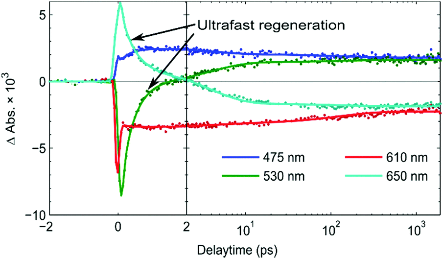 | ||
| Fig. 5 Kinetics of the fs TAS signal of NiO-PB6-TiO2 at significant wavelengths after excitation at 560 nm. | ||
Hole and electron injection observed by fs-TAS are indeed occurring on a much faster time scale than the instrument resolution of TCSPC (30 ps). It explains why steady state fluorescence intensity is much more quenched than expected from the TCSPC lifetime measurements. From the fs-TAS data we estimate hole and electron injection efficiencies up to 99.9% and 93%, respectively, assuming that all ultrafast quenching is due to charge separation (see Table S3, ESI†).
During the formation of the Stark effect signal, the transient absorption at 475 nm and 610 nm only shows minor changes in the fs-TAS measurement window. No clear decay has been observed in the fs-TAS and the kinetic traces. It indicates that relatively long-lived electrons and holes can be localized in TiO2 and NiO semiconductors, respectively, for more than 1.9 ns without noticeable recombination. This is in contrast to the NiO-PB6 sample (see Fig. S12, ESI†), where most of the signal of the reduced PB6− decays much faster; a bi-exponential fit gives lifetimes of 6 ps and 90 ps. The long lived signal for NiO-PB6-TiO2 is surprising in comparison to the recent electron transfer study in amorphous TiO2 system with a covalently linked dye, where up to 60% of the oxidized dye recombined in 220 ps.34
Conclusions
A dye sensitized NiO–dye–TiO2 core–shell architecture film was successfully fabricated for the first time. TEM measurements confirmed that the NiO nanoparticles were covered by a conformal TiO2 layer, allowing both close contact between the dye and semiconductors and “well-oriented” dye alignment for optimal electron/hole injection. The dye was observed to be rather stable during ALD process. This film architecture renders ultrafast and efficient hole injection (>98%, ≤200 fs) and dye regeneration (70–93%, ≤500 fs) proven by the appearance of a spectrally pronounced charge separated state (Stark effect). The recombination in the core–shell NiO–dye–TiO2 structure was found to be much slower than that of the conventional dye sensitized NiO film. The efficient charge separation and dye regeneration make this architecture interesting for further applications in solid state DSSCs as well as in dye sensitized solar fuel devices.Conflicts of interest
The authors declare no competing financial interests.Acknowledgements
The authors thank the finical support from KA Wallenberg Foundation (grant no. 2011.0067) and Swedish Energy Agency (grant no. 43599-1). The authors also give their great gratitude to Luca D'Amario and Leif Häggman for offering NiO and ZrO2 paste, respectively and to Prof. Sascha Ott for his help with HRMS test. Lei Tian also thanks China Scholarship Council (CSC) for the scholarship support.References
- B. O’regan and M. Grätzel, Nature, 1991, 353, 737 CrossRef.
- J. He, H. Lindström, A. Hagfeldt and S.-E. Lindquist, J. Phys. Chem. B, 1999, 103, 8940 CrossRef CAS.
- A. Y. Anderson, P. R. Barnes, J. R. Durrant and B. C. O’Regan, J. Phys. Chem. C, 2011, 115, 2439 CAS.
- J. N. Clifford, E. Palomares, M. K. Nazeeruddin, M. Grätzel and J. R. Durrant, J. Phys. Chem. C, 2007, 111, 6561 CAS.
- A. Morandeira, G. Boschloo, A. Hagfeldt and L. Hammarström, J. Phys. Chem. C, 2008, 112, 9530 CAS.
- Y. Hao, W. Yang, L. Zhang, R. Jiang, E. Mijangos, Y. Saygili, L. Hammarström, A. Hagfeldt and G. Boschloo, Nat. Commun., 2016, 7, 13934 CrossRef CAS PubMed.
- S. J. Simon, F. G. Parlane, W. B. Swords, C. W. Kellett, C. Du, B. Lam, R. K. Dean, K. Hu, G. J. Meyer and C. P. Berlinguette, J. Am. Chem. Soc., 2016, 138, 10406 CrossRef CAS PubMed.
- L. Casarin, W. B. Swords, S. Caramori, C. A. Bignozzi and G. J. Meyer, Inorg. Chem., 2017, 56, 7324 CrossRef CAS PubMed.
- W. B. Swords, G. Li and G. J. Meyer, Inorg. Chem., 2015, 54, 4512 CrossRef CAS PubMed.
- L. J. Antila, P. Myllyperkio, S. Mustalahti, H. Lehtivuori and J. Korppi-Tommola, J. Phys. Chem. C, 2014, 118, 7772 CAS.
- L. Zhang, G. Boschloo, L. Hammarström and H. Tian, Phys. Chem. Chem. Phys., 2016, 18, 5080 RSC.
- A. Morandeira, G. Boschloo, A. Hagfeldt and L. Hammarström, J. Phys. Chem. B, 2005, 109, 19403 CrossRef CAS PubMed.
- P. Qin, J. Wiberg, E. A. Gibson, M. Linder, L. Li, T. Brinck, A. Hagfeldt, B. Albinsson and L. Sun, J. Phys. Chem. C, 2010, 114, 4738 CAS.
- E. Sheibani, L. Zhang, P. Liu, B. Xu, E. Mijangos, G. Boschloo, A. Hagfeldt, L. Hammarström, L. Kloo and H. Tian, RSC Adv., 2016, 6, 18165 RSC.
- Y. Yu, K. A. Click, S. M. Polen, M. He, C. M. Hadad and Y. Wu, J. Phys. Chem. C, 2017, 121, 20720 CAS.
- Y. Tachibana, J. E. Moser, M. Grätzel, D. R. Klug and J. R. Durrant, J. Phys. Chem., 1996, 100, 20056 CrossRef CAS.
- N. J. Cherepy, G. P. Smestad, M. Grätzel and J. Z. Zhang, J. Phys. Chem. B, 1997, 101, 9342 CrossRef CAS.
- K. H. Wong, K. Ananthanarayanan, S. R. Gajjela and P. Balaya, Mater. Chem. Phys., 2011, 125, 553 CrossRef CAS.
- Y.-M. Lee and C.-H. Lai, Solid-State Electron., 2009, 53, 1116 CrossRef CAS.
- J. Bandara and H. Weerasinghe, Sol. Energy Mater. Sol. Cells, 2005, 85, 385 CrossRef CAS.
- H.-J. Son, C. Prasittichai, J. E. Mondloch, L. Luo, J. Wu, D. W. Kim, O. K. Farha and J. T. Hupp, J. Am. Chem. Soc., 2013, 135, 11529 CrossRef CAS PubMed.
- R. J. Kamire, M. B. Majewski, W. L. Hoffeditz, B. T. Phelan, O. K. Farha, J. T. Hupp and M. R. Wasielewski, Chem. Sci., 2017, 8, 541 RSC.
- K. Hanson, M. D. Losego, B. Kalanyan, D. L. Ashford, G. N. Parsons and T. J. Meyer, Chem. Mater., 2012, 25, 3 CrossRef.
- L. Alibabaei, M. K. Brennaman, M. R. Norris, B. Kalanyan, W. Song, M. D. Losego, J. J. Concepcion, R. A. Binstead, G. N. Parsons and T. J. Meyer, Proc. Natl. Acad. Sci. U. S. A., 2013, 110, 20008 CrossRef CAS PubMed.
- L. Alibabaei, B. D. Sherman, M. R. Norris, M. K. Brennaman and T. J. Meyer, Proc. Natl. Acad. Sci. U. S. A., 2015, 112, 5899 CrossRef CAS PubMed.
- G. Natu, Z. Huang, Z. Ji and Y. Wu, Langmuir, 2011, 28, 950 CrossRef PubMed.
- C. Prasittichai and J. T. Hupp, J. Phys. Chem. Lett., 2010, 1, 1611 CrossRef CAS.
- D. Gosztola, M. P. Niemczyk, W. Svec, A. S. Lukas and M. R. Wasielewski, J. Phys. Chem. A, 2000, 104, 6545 CrossRef CAS.
- A. Osuka, N. Mataga and T. Okada, Pure Appl. Chem., 1997, 69, 797 CrossRef CAS.
- P. Qin, H. Zhu, T. Edvinsson, G. Boschloo, A. Hagfeldt and L. Sun, J. Am. Chem. Soc., 2008, 130, 8570 CrossRef CAS PubMed.
- L. D’Amario, L. J. Antila, B. Pettersson Rimgard, G. Boschloo and L. Hammarström, J. Phys. Chem. Lett., 2015, 6, 779 CrossRef PubMed.
- I. S. Kim, R. T. Haasch, D. H. Cao, O. K. Farha, J. T. Hupp, M. G. Kanatzidis and A. B. Martinson, ACS Appl. Mater. Interfaces, 2016, 8, 24310 CAS.
- I. S. Kim, D. H. Cao, D. B. Buchholz, J. D. Emery, O. K. Farha, J. T. Hupp, M. G. Kanatzidis and A. B. Martinson, Nano Lett., 2016, 16, 7786 CrossRef CAS PubMed.
- M. K. Gish, A. M. Lapides, M. K. Brennaman, J. L. Templeton, T. J. Meyer and J. M. Papanikolas, J. Phys. Chem. Lett., 2016, 7, 5297 CrossRef CAS PubMed.
- J. Chavez, R. Devine and L. Koltunski, J. Appl. Phys., 2001, 90, 4284 CrossRef CAS.
Footnotes |
| † Electronic supplementary information (ESI) available: Synthesis and characterization of PB6; experimental details including sample preparation and measurements. See DOI: 10.1039/c7cp07088h |
| ‡ These authors contribute equally. |
| This journal is © the Owner Societies 2018 |