 Open Access Article
Creative Commons Attribution 3.0 Unported Licence
Room-temperature film formation of metal halide perovskites on n-type metal oxides: the catalysis of ZnO on perovskite crystallization†
Zhongcheng
Yuan
 a,
Sai
Bai
 *a,
Zhibo
Yan
ab,
Jun-Ming
Liu
b and
Feng
Gao
 *a
*a
aDepartment of Physics, Chemistry and Biology (IFM), Linköping University, Linköping, SE-58183, Sweden. E-mail: sai.bai@liu.se; feng.gao@liu.se
bLaboratory of Solid State Microstructures and Innovation, Center of Advanced Microstructures, Nanjing University, Nanjing 210093, P. R. China
First published on 11th May 2018
Abstract
We investigate the effect of commonly used solution-processed TiOx, SnO2 and ZnO interlayers on the perovskite film crystallization process. We find that the ZnO/perovskite interface can efficiently catalyze the perovskite crystallization even without thermal annealing.
Metal halide perovskites have emerged as promising materials for a range of optoelectronic applications, including solar cells and light-emitting diodes (LEDs).1–3 In a typical perovskite solar cell or LED device, n-type metal oxide films, such as solution-processed TiOx,4 SnO25 and ZnO,6 are widely used as electron-transport layers (ETLs) to facilitate perovskite crystallization and enable efficient electron extraction/injection at the interface. Solution-processed ZnO with suitable energy levels and optoelectronic properties hence has been successfully employed in optoelectronic devices processed from organic and quantum dot semiconductors.7,8 However, perovskite optoelectronic devices processed on ZnO, especially perovskite solar cells, always exhibit inferior device performance and poor stability compared with those on TiO2 and SnO2.9 Recently, it has been demonstrated that with proper surface modification via functional interlayers the interfacial reaction between perovskite films and ZnO can be efficiently surpassed, leading to obviously improved device efficiencies of perovskite solar cells and LEDs.10–12 Unfortunately, the operational stability of ZnO-based perovskite optoelectronic devices is still moderate. Considering the recent advances of the use of ZnO in perovskite optoelectronic devices, a deep understanding of the interaction between perovskites and ZnO is expected to give more insights into further improving the device stability.
In previous studies, detailed theoretical calculations have been performed to explain the chemical instability of the ZnO/perovskite interface, and many hypotheses have been proposed to reveal the possible decomposition paths. It is well-accepted that the basic nature of ZnO may facilitate the proton-transfer reactions at the ZnO/perovskite interface, resulting in the destruction of the perovskite crystal structure during thermal annealing.9 In addition, the residual functional groups at the surface of solution-processed ZnO, e.g. hydroxyl groups and acetate ligands, accelerate the interfacial reaction at elevated temperatures, resulting in a fast thermal decomposition of perovskites to PbI2.9 Unlike the well-investigated perovskite decomposition process on ZnO, the effect of the ZnO/perovskite interface on the perovskite crystallization process has rarely been reported. This is mainly due to the simultaneous decomposition and crystallization processes of perovskites that occurred on ZnO under thermal annealing, making it hard to distinguish the two processes.
Herein, with the introduction of a room-temperature vacuum-processing method, we decouple the film decomposition and crystallization processes of perovskites on n-type metal oxide substrates. We systemically investigate the film formation of the methylammonium lead iodide (MAPbI3) perovskite on commonly used metal oxide ETLs, i.e. TiOx, SnO2, and ZnO. Through the optical and structural characterization of the resulting perovskite films, we find that the reaction at the ZnO/perovskite interface occurs at the beginning of the perovskite crystallization process. With the removal of the organic components during vacuum-processing, only the films processed on ZnO exhibit good perovskite crystallinity, while the crystallization of MAPbI3 on TiOx and SnO2 is obviously retarded. The good photoluminescence (PL) of the films and decent device performance indicate the excellent optoelectronic properties of the resulting perovskite films on ZnO. Our observations reveal that the reaction at the ZnO/perovskite interface does exist even without any impetus from thermal annealing, helping to catalyse the perovskite crystallization process. In addition, we also demonstrate that with the modification of ZnO using an interfacial polymeric surface modifier of polyethylenimine ethoxylated (PEIE), the ZnO/PEIE interface exhibits similar surface properties to TiOx and SnO2. This leads to efficient suppression of the interfacial reaction that occurred between ZnO and the perovskite.
To prepare the metal oxide substrates, SnO2, a TiOx precursor solution and ZnO nanoparticle dispersion are prepared and deposited on pre-cleaned ITO substrates according to previous studies.1,5,13 The perovskite films are deposited on the different n-type metal oxides via a solvent quenching method in a glovebox, with dimethylformamide (DMF) as the precursor solvent and toluene as the anti-solvent.4 For the vacuum-processed films, the as-spun films are placed in a vacuum chamber (−1 bar) and kept in the dark at room temperature for 12 h (see details in the experimental section of the ESI†).
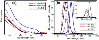
We carried out a range of film characterization studies to investigate the perovskite formation process on the different metal oxides. Fig. 1a shows the ultraviolet-visible (UV-vis) absorption spectra of the perovskite films deposited on the TiOx, SnO2 and ZnO substrates before and after vacuum-processing. We notice that there is negligible change in the film absorption on TiOx and SnO2 before and after vacuum-processing and no absorption from the crystallized perovskite is detected. Surprisingly, although the absorption of the as-spun perovskite film on ZnO is similar to those on TiOx and SnO2, a clear absorption from the crystallized perovskites is observed after vacuum processing. The optical bandgap of the film calculated using a Tauc plot of the absorption spectra is ∼1.60 eV, which matches well with that of the MAPbI3 perovskite. Fig. 1b shows the photoluminescence (PL) spectra of the thin films deposited on the different metal oxides before and after vacuum processing. We observe only one typical PL emission peak located at around 680 nm of the as-spun films on TiOx and SnO2. The PL peaks show slight red shift to 702 nm after vacuum processing. In contrast, for the as-spun film on ZnO, we clearly observe two emission peaks in the PL spectrum, one located at ∼718 nm and another at ∼780 nm, which can be attributed to the intermediate phase and crystalized MAPbI3 perovskite, respectively. After vacuum-processing, the PL emission at ∼718 nm disappears and the PL emission from the perovskite becomes dominant, implying the efficient formation of well crystallized MAPbI3 perovskites on the ZnO substrates. The red shift of the PL spectra may be attributed to the promoted crystallization and enlarged grain sizes of the perovskites on ZnO during the vacuum processing. The PL intensity of the perovskite film processed on ZnO is also much higher than that on TiOx and SnO2, suggesting better crystallinity of perovskites processed on ZnO (see the inset PL spectra in Fig. 1b). We conclude from the optical characterization results that crystalline perovskite films form only on ZnO under room-temperature vacuum-processing, while the perovskite crystallization process is significantly inhibited on the TiOx and SnO2 metal oxide substrates.
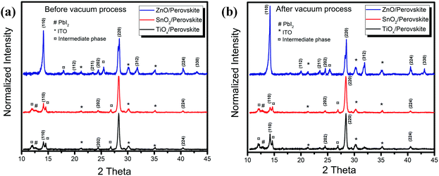
To further investigate the crystal structure changes of the perovskites on the different metal oxide substrates, we performed the X-ray diffraction (XRD) measurements, and Fig. 2 shows the results. From the XRD patterns of the thin films on TiOx and SnO2, we only observe slight enhancement of the intensity but little changes in the typical peaks before and after vacuum processing. The crystal properties are almost the same on these two metal oxides, which is consistent with the characterization results of the absorption and PL spectra. We attribute the weak peaks at 14.1° and 28.3° to the (110) and (220) planes of the tetragonal phase MAPbI3 perovskite, respectively. We also detect the typical peak corresponding to PbI2 at 12.8° together with possible intermediate phases of PbI2-MAI-DMF at 13.1° from the films on TiOx and SnO2.14,15 However, the as-deposited film on ZnO exhibits a much higher XRD intensity of the crystalline perovskite and produces a preferential orientation of the (110) plane after vacuum-processing. Since we use the anti-solvent to promote the fast perovskite crystallization during the film deposition, we assume that the as-spun films consist of a large amount of small perovskite crystals along with the intermediate phases.16 The different XRD results of the as-spun films on the different metal oxides reveal that the perovskite crystallization depends strongly on the surface properties of the bottom substrates. The effect of ZnO on the perovskite crystallization starts from the initial perovskite crystallization stage, leading to more obvious crystalline perovskite formation. We observe that further crystallization and coarsening of the perovskite proceed during the vacuum-processing with the removal of excess organic components (Fig. S1, ESI†). However, without enough driving force from the thermal annealing, the perovskite crystallization on TiOx and SnO2 is retarded, while the interfacial reaction at the ZnO/perovskite interface catalyses the perovskite crystallization.
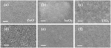
The promoted film crystallization and enlarged grain sizes of the perovskite on ZnO are further confirmed by scanning electron microscopy (SEM) characterization studies, shown in Fig. 3. We compare the top-view SEM images of the films on the different substrates before and after vacuum-processing. We observe slightly enhanced crystallinity from the as-spun films on ZnO compared with those on TiOx and SnO2. For the vacuum processed films, we clearly find that the crystallization of the perovskite is much obvious on the ZnO substrates with grains larger than 300 nm. In comparison, the perovskite crystallization is significantly suppressed on the TiOx and SnO2 substrates, which is consistent with our XRD results.
 | ||
| Fig. 3 SEM images of perovskite films deposited on ZnO, SnO2 and TiOx substrates before (a–c) and after (d–f) vacuum-processing, respectively. The scale bar is 1 μm. | ||
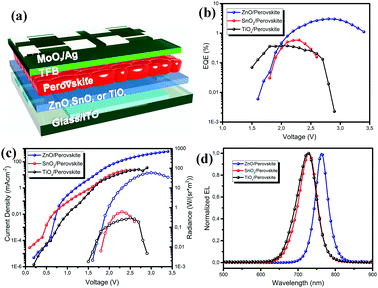
To investigate the optoelectronic properties of the obtained perovskite films, we fabricated perovskite LEDs based on the vacuum-processed perovskite films on these three metal oxides. The ZnO, SnO2 and TiOx films in the LEDs function as electron injection layers, while the commonly used poly(9,9-dioctyl-fluorene-co-N-(4-butylphenyl)diphenylamine) (TFB) is deposited on top of the perovskite films as the hole injection layer (the device geometry is shown in Fig. 4a). We note that although the top view of the perovskite on ZnO shows many voids, the cross-sectional SEM images of the perovskite (shown in Fig. S2, ESI†) demonstrate a continuous layer. The external quantum efficiency–voltage (EQE–V) curves and the current density–voltage–radiance (J–V–R) curves are depicted in Fig. 4b and c. The maximum EQE, maximum radiance, EL peak and turn on voltage (Vth) values of the devices based on the different substrates are all summarized in Table 1. The devices based on SnO2 and TiOx exhibit poor performance with EQEs less than 1%, while the ZnO-based perovskite LEDs show much improved device performance, with a maximum EQE of 3.03% at 2.8 V and a high radiance of 58.8 W (sr−1 m−2). The normalized EL spectra of the LEDs on the different substrates are depicted in Fig. 3d (all obtained at 2.5 V). The EL peak of the device based on ZnO is located at 762.4 nm, which is consistent with the emission from the MAPbI3 perovskite. We observe that the EL emission peaks for the devices on SnO2 and TiOx are significantly blue-shifted to around 725 nm. The decent device performance further confirms the good optoelectronic properties of the vacuum-processed perovskite films on ZnO.
| Device | EQE (%) | Radiance (W (sr−1 m−2)) | EL peak (nm) | V th (V) |
|---|---|---|---|---|
| ZnO | 3.03 | 58.8 | 762.4 | 1.6 |
| SnO2 | 0.58 | 0.6 | 728.8 | 1.8 |
| TiOx | 0.37 | 0.3 | 725.8 | 1.5 |
In previous reports, solution-processed ZnO was proven to be capable of accelerating the decomposition process of perovskite films under thermal annealing.9 We believe that the deprotonation of the organic cations at the perovskite/ZnO interface under mild conditions is helpful in initiating and promoting the perovskite crystallization. In addition, since ZnO is synthesized from acetate salts and the surface ligands cannot be completely removed,8 we also need to note the effect of the residual acetate ligands of ZnO on the perovskite crystallization. It has been well demonstrated that the introduction of trace amounts of acetate-based additives could decrease the activation energy (Ea) of perovskite crystallization.17,18 In addition, the incorporation of lead acetate into a perovskite precursor solution can also promote the formation of dense and continuous films.16,19,20 We anticipate that the surface acetate ligands of ZnO have similar effects to acetate ions in the precursor on reducing the Ea, promoting the perovskite crystallization.
We notice that PEIE is commonly used to modify the surface of ZnO for efficient perovskite optoelectronic devices, especially perovskite LEDs. To verify the effect of PEIE modification on ZnO substrates, we performed the same vacuum-processing of perovskite films on ZnO/PEIE substrates. We followed the optimized recipe for efficient perovskite LEDs and introduced a thin layer of PEIE (0.04 wt%) on top of the ZnO film. We carried out detailed optical and structural characterization studies on the films before and after vacuum-processing, and Fig. S3–S5 (ESI†) show the results. We find that with the insertion of a thin PEIE layer the perovskite crystallization process on ZnO/PEIE behaves similarly to those on TiOx and SnO2. The obtained perovskite films exhibit the same retarded optical and structural properties and film morphology.
In conclusion, we investigated the perovskite film formation process on commonly used n-type metal oxides under room-temperature vacuum-processing. We observed a much different crystallization process of perovskites on ZnO from those on TiOx and SnO2. We anticipate that the chemical interaction at the ZnO/perovskite interface, from either the basic nature of ZnO or the residual acetate ligands, can decrease the activation energy for the perovskite crystallization. With the introduction of a thin PEIE surface modifier, the interaction between ZnO and perovskites can be efficiently suppressed, leading to retarded perovskite crystallization and crystal growth. Our results reveal the effect of interaction at the ZnO/perovskite interface on the perovskite crystallization and provide new insights into further development of ZnO-based perovskite optoelectronic devices.
This work was supported by an ERC Starting Grant (717026), the Carl Tryggers Stiftelse, and the European Commission Marie Skłodowska-Curie Actions (691210). Z. Y. also acknowledges the financial support from the China Scholarship Council. S. B. and Z. Y. are supported by VINNMER Marie Curie Fellowships.
Conflicts of interest
The authors declare no competing financial interest.Notes and references
- N. Wang, L. Cheng, R. Ge, S. Zhang, Y. Miao, W. Zou, C. Yi, Y. Sun, Y. Cao and R. Yang, Nat. Photonics, 2016, 10, 699 CrossRef.
- Z. Xiao, R. A. Kerner, L. Zhao, N. L. Tran, K. M. Lee, T.-W. Koh, G. D. Scholes and B. P. Rand, Nat. Photonics, 2017, 11, 108 CrossRef.
- M. Yuan, L. N. Quan, R. Comin, G. Walters, R. Sabatini, O. Voznyy, S. Hoogland, Y. Zhao, E. M. Beauregard and P. Kanjanaboos, Nat. Nanotechnol., 2016, 11, 872 CrossRef PubMed.
- N. J. Jeon, J. H. Noh, Y. C. Kim, W. S. Yang, S. Ryu and S. I. Seok, Nat. Mater., 2014, 13, 897 CrossRef PubMed.
- Q. Jiang, L. Zhang, H. Wang, X. Yang, J. Meng, H. Liu, Z. Yin, J. Wu, X. Zhang and J. You, Nat. Energy, 2017, 2, 16177 CrossRef.
- D. Liu and T. L. Kelly, Nat. Photonics, 2014, 8, 133 CrossRef.
- X. Dai, Z. Zhang, Y. Jin, Y. Niu, H. Cao, X. Liang, L. Chen, J. Wang and X. Peng, Nature, 2014, 515, 96 CrossRef PubMed.
- S. Bai, Y. Jin, X. Liang, Z. Ye, Z. Wu, B. Sun, Z. Ma, Z. Tang, J. Wang and U. Wuerfel, Adv. Energy Mater., 2015, 5, 1401606 CrossRef.
- J. Yang, B. D. Siempelkamp, E. Mosconi, F. De Angelis and T. L. Kelly, Chem. Mater., 2015, 27, 4229 CrossRef.
- Y. Cheng, Q.-D. Yang, J. Xiao, Q. Xue, H.-W. Li, Z. Guan, H.-L. Yip and S.-W. Tsang, ACS Appl. Mater. Interfaces, 2015, 7, 19986 Search PubMed.
- J. Wang, N. Wang, Y. Jin, J. Si, Z. K. Tan, H. Du, L. Cheng, X. Dai, S. Bai and H. He, Adv. Mater., 2015, 27, 2311 CrossRef PubMed.
- J. Kim, G. Kim, T. K. Kim, S. Kwon, H. Back, J. Lee, S. H. Lee, H. Kang and K. Lee, J. Mater. Chem. A, 2014, 2, 17291 Search PubMed.
- Z. Yuan, Z. Wu, S. Bai, Z. Xia, W. Xu, T. Song, H. Wu, L. Xu, J. Si and Y. Jin, Adv. Energy Mater., 2015, 5, 1500038 CrossRef.
- B. Duan, Y. Ren, Y. Xu, W. Chen, Q. Ye, Y. Huang, J. Zhu and S. Dai, Inorg. Chem. Front., 2017, 4, 473 RSC.
- X. Guo, C. McCleese, C. Kolodziej, A. C. Samia, Y. Zhao and C. Burda, Dalton Trans., 2016, 45, 3806 RSC.
- N. K. Noel, M. Congiu, A. J. Ramadan, S. Fearn, D. P. McMeekin, J. B. Patel, M. B. Johnston, B. Wenger and H. J. Snaith, Joule, 2017, 1, 328 CrossRef.
- D. T. Moore, H. Sai, K. W. Tan, D.-M. Smilgies, W. Zhang, H. J. Snaith, U. Wiesner and L. A. Estroff, J. Am. Chem. Soc., 2015, 137, 2350 CrossRef PubMed.
- Q. Wu, P. Zhou, W. Zhou, X. Wei, T. Chen and S. Yang, ACS Appl. Mater. Interfaces, 2016, 8, 15333 Search PubMed.
- D. B. Liu, G. Wang, F. Wu, R. Wu, T. Chen, B. F. Ding and Q. L. Song, Org. Electron., 2017, 43, 189 CrossRef.
- W. Zhang, M. Saliba, D. T. Moore, S. K. Pathak, M. T. Hörantner, T. Stergiopoulos, S. D. Stranks, G. E. Eperon, J. A. Alexander-Webber and A. Abate, Nat. Commun., 2015, 6, 6142 CrossRef PubMed.
Footnote |
| † Electronic supplementary information (ESI) available. See DOI: 10.1039/c8cc02482k |
| This journal is © The Royal Society of Chemistry 2018 |


