Quantification of effective thermal conductivity in the annealing process of Cu2ZnSn(S,Se)4 solar cells with 9.7% efficiency fabricated by magnetron sputtering†
Woo-Lim
Jeong‡
 ab,
Jung-Hong
Min‡
ab,
Hae-Sun
Kim
ab,
Ji-Hun
Kim
a,
Jin-Hyeok
Kim
c and
Dong-Seon
Lee
*ab
ab,
Jung-Hong
Min‡
ab,
Hae-Sun
Kim
ab,
Ji-Hun
Kim
a,
Jin-Hyeok
Kim
c and
Dong-Seon
Lee
*ab
aSchool of Electrical Engineering and Computer Science, Gwangju Institute of Science and Technology, Gwangju 61005, South Korea. E-mail: dslee66@gist.ac.kr
bResearch Institute for Solar and Sustainable Energies, Gwangju 61005, South Korea
cOptoelectronics Convergence Research Center, Chonnam National University, 300 Youngbong-Dong, Puk-Gu, Gwangju 61186, South Korea
First published on 21st February 2018
Abstract
Cu2ZnSn(S,Se)4 (CZTSSe) has attracted much attention as the absorption layer of photovoltaic devices because of its appropriate bandgap energy and low cost. However, CZTSSe solar cells have so far shown low power conversion efficiency compared to other solar cells and studies are being conducted to improve it. In this study, we achieved an improvement in the shunt resistance and power conversion efficiency (PCE) of CZTSSe solar cells with quantification of the effective thermal conductivity. A CZTSSe solar cell fabricated using a graphite box designed with high thermal conductivity exhibited a high shunt resistance of 413 Ω cm2 and a fill factor of 63.8%, and additionally, secondary phases such as Cu2S/Se and CuS/Se were not detected. On the other hand, a CZTSSe solar cell fabricated using a graphite box with low thermal conductivity showed a rougher surface and low shunt resistance mainly related to secondary phase formation. As a result, a PCE of 9.72% was achieved using a graphite box designed with high thermal conductivity.
1. Introduction
Silicon, GaAs, and Cu(In,Ga)(Se,S)2 (CIGS) solar cells have been actively studied in recent decades for use as an eco-friendly energy source. Among the single junction solar cells, crystalline silicon, group III–V GaAs, and CIGS solar cells showed a high power conversion efficiency (PCE) of 26.7%, 28.8%, and 21.7%, respectively.1–4 However, to promote the use of solar cells, the fabrication process should ultimately use earth-abundant elements without toxic materials. The deposits of rare metals such as In or Ga are limited, and As is toxic. Hence, in recent years, CZTSSe solar cells that use earth-abundant elements without toxic materials have been studied.CZTSSe solar cells have a relatively low PCE of 12.6% compared to other solar cells,5 so many studies have recently been conducted to improve the efficiency of CZTSSe solar cells. Giraldo et al. reported a high open circuit voltage (VOC) and 10.6% PCE of Cu2ZnSnSe4 (CZTSe) solar cells using a Ge superficial nanolayer,6 and Kim et al. obtained a low VOC deficit and 8.65% PCE for CZTSe solar cells using an Al2O3 passivation layer on the top and bottom interfaces of the CZTSe absorber fabricated by thermal co-evaporation.7 In addition, without an additional fabrication process, Li et al. achieved 10.2% PCE for CZTSSe solar cells through controlling the Zn/Sn ratio of the CZTSSe absorber prepared by magnetron sputtering,8 while Gang et al. obtained a CZTSSe solar cell PCE of 9.24% by precise control of the Se and S vapor pressure.9 However, previous studies have not provided sufficient information on the formation of the CZTSSe absorber and effective heat transfer, which have been found to play an important role in solar cell performance.
In this study, we quantified the effective thermal conductivity such as the cooling rate constant of the graphite box used for the sulfo-selenization process and investigated the characteristics of the CZTSSe solar cells. As far as we know, this is the first time that the analysis of the effective heat transfer of graphite boxes has been performed. A CZTSSe solar cell fabricated with a graphite box designed with high thermal conductivity showed a lower root-mean-square roughness (Rq) and a higher fill factor (FF). Furthermore, secondary phases such as CuS and CuSe known to have a detrimental effect on solar cell performance were not detected. As a result, CZTSSe solar cells with a best performance of 9.72% were obtained, which was additionally certified by an accredited laboratory (Korea Institute of Energy Research, KIER).
2. Experimental section
2.1 Characterization of the graphite boxes
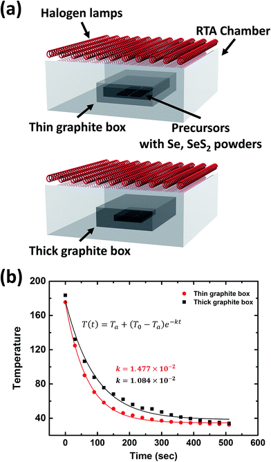
Analysis of the graphite boxes was conducted prior to the CZTSSe absorber layer preparation process. The weights of the thin and thick graphite boxes used in the CZTSSe absorber layer annealing process (Fig. 1a) were 156.4 g and 241.6 g, respectively. In order to analyze the thermal characteristics, the boxes were heated up to 200 °C using a hot plate and then allowed to cool down to room temperature; the temperature was periodically measured with a thermocouple. In Fig. 1b, the solid lines show the results of exponentially fitting the data. The measurements were carried out in an environment that minimized convection and thermal radiation effects, and it is assumed that Newton's law of cooling was valid for each measurement. Under these assumptions, one can writewhere T is the temperature of the graphite box, Tenv is the temperature of the environment around the graphite box, and k is the cooling rate constant of the graphite box. Under the initial condition T(0) = T0, the solution is given by
| T(t) = Ta + (T0 − Ta)e−kt. |
Using this, the cooling rate constants of the thin and thick graphite boxes were found to be 1.477 × 10⁻² s−1 and 1.084 × 10⁻² s−1, respectively. Therefore, the thin and thick graphite boxes had high thermal conductivity (HTC) and low thermal conductivity (LTC), respectively.
2.2 Formation of the CZTSSe absorber layers
The Mo layer used as a back electrode was deposited on soda-lime glass using a DC magnetron sputtering method at a sputtering power of 280 W (10.85 W cm−2) in an argon atmosphere at a pressure of 1.33 Pa for 220 s followed by 0.13 Pa for 5000 s. Afterwards, Zn, Cu, and Sn layers were sequentially deposited on the Mo layer. The stacking order was determined to minimize the negative effects of the rough Sn surface, as reported in our previous study.10 DC magnetron sputtering was used for the deposition of the zinc and copper layers and RF magnetron sputtering for the Sn layers. Each metal layer was deposited using 50 W (1.10 W cm−2) sputtering power in an argon atmosphere at a pressure of 0.4 Pa. Under these conditions, three different precursors were prepared by changing the Zn deposition time. The precursors were sulfo-selenized with 0.5 g of Se and 0.04 g of SeS2 powders in either the HTC or the LTC graphite boxes using rapid thermal annealing (RTA). This method of forming CZTSSe absorber layers using a SeS2 source has been reported to result in bandgap grading effects and increased VOC.11 The RTA chamber was evacuated for three minutes using a rotary pump before the annealing process to remove any unwanted elements and then filled with argon gas to 50 kPa. During the annealing process, the precursors were heated from room temperature to 300 °C in 1000 s and then maintained at 300 °C for 1500 s. Next, they were heated from 300 °C to 530 °C in 1000 s and then maintained at 530 °C for 1100 s.2.3 Fabrication of the CdS buffer and window layers, and electrode
The CZTSSe absorber films were immersed in 0.05 M aqueous KCN solution for 5 minutes to remove the secondary phase and then rinsed with deionized water. After this, a 70 nm CdS buffer layer was deposited by chemical bath deposition at 80 °C. Right after the CdS deposition, 50 nm intrinsic ZnO and 350 nm aluminum-doped ZnO window layers were deposited using RF magnetron sputtering at room temperature and 150 °C, respectively, and then a 50 nm Ni and 500 nm Al electrode was deposited through a shadow mask with an electron beam evaporator. This was followed by deposition of a 100 nm thick MgF2 anti-reflection coating.2.4 Characterization
Scanning electron microscopy (SEM, Hitachi S-4700), energy dispersive X-ray spectroscopy (EDX) and atomic force microscopy (AFM, XE-100, Park Systems) were used for the surface analysis of the CZTSSe absorber layers prepared under different annealing conditions. Park Systems AFM XEI software programming was used to calculate the Rq values and analyze the cross-sectional height profiles. Raman scattering measurements were performed at a laser excitation wavelength of 514 nm. The PCE and solar cell parameters of the CZTSSe solar cells were measured with a class AAA solar simulator (WXS-155S-L2, WACOM, Japan) under conditions of AM 1.5G, 100 mW cm−2, and 25 °C. The external quantum efficiency (EQE) and capacitance–voltage measurements were performed with a PV Measurements QEX7 system and a precision LCR meter (Agilent 4284A) at room temperature, respectively. High-angle annular dark-field scanning transmission electron microscopy (HAADF STEM) was performed on a JEM-2100F HR transmission electron microscope coupled with an EDX.3. Results and discussion
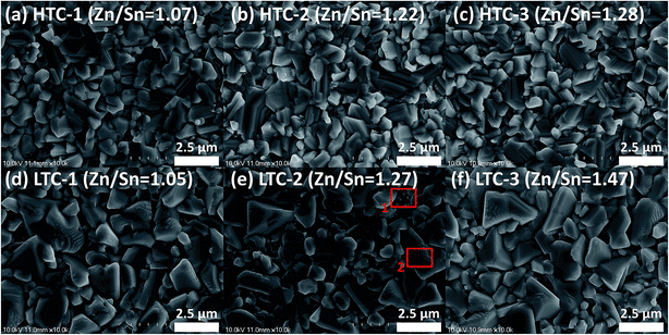
An SEM analysis was performed to analyze the CZTSSe absorber layers fabricated by sulfo-selenization with the HTC and LTC graphite boxes. They were made by changing the Zn/Sn ratio (their compositional ratio data can be found in the ESI in Table S1†). As shown in Fig. 2a–c, the CZTSSe absorber layers prepared by HTC annealing had a small grain size whereas those fabricated under LTC annealing conditions had a large grain size (Fig. 2d–f). In addition, very small grains with a size of several tens of nanometers and a valley region were formed between the large grains. In order to determine the compositional ratio of the grains, EDX analysis was conducted on regions 1 and 2 of the LTC-2 sample (see Fig. S1†). 23.94 at% Zn, 29.59 at% S, and 31.51 at% Se were detected in region 1; thus the very small grains might have been composed of mainly ZnS and ZnSe. It has previously been shown that the secondary phases of CZTSSe solar cells act as shunting paths and are harmful to carrier collection.12,13 The secondary phases are also known to be formed at temperatures lower than the CZTSSe formation temperature,14 and are more likely to be formed during the long cooling time under LTC annealing conditions. The compositional ratio of the large grain in region 2 was found to be Zn/Sn = 1.14, Cu/(Zn + Sn) = 0.93, and (S + Se)/metals = 1.03. It is known that CZTSSe solar cells with a Cu-poor/Zn-rich composition exhibit better device performance; this is accepted as the empirical rule.15,16From the SEM results in Fig. 2, we identified that the CZTSSe absorber layers fabricated under HTC annealing conditions have a flatter surface than those fabricated under LTC conditions. Therefore, AFM measurements were conducted to determine the surface roughness and depths of the valleys accurately (Fig. 3). The Rq of HTC-1, HTC-2 and HTC-3 CZTSSe absorber layers was 133.9, 117.2, and 119.4 nm, respectively. On the other hand, LTC-1, LTC2 and LTC-3 CZTSSe absorber layers showed a rougher surface (165.6, 222.8, and 209.4 nm, respectively). This tendency toward surface roughness was also confirmed by analyzing the height profiles. The depths of the valleys in the HTC samples were up to 600 nm whereas those in the LTC samples were up to 800 nm. The deep valleys of the LTC samples might have acted as shunting paths, thereby decreasing the shunt resistance (RSH) and PCE of the solar cell.17,18
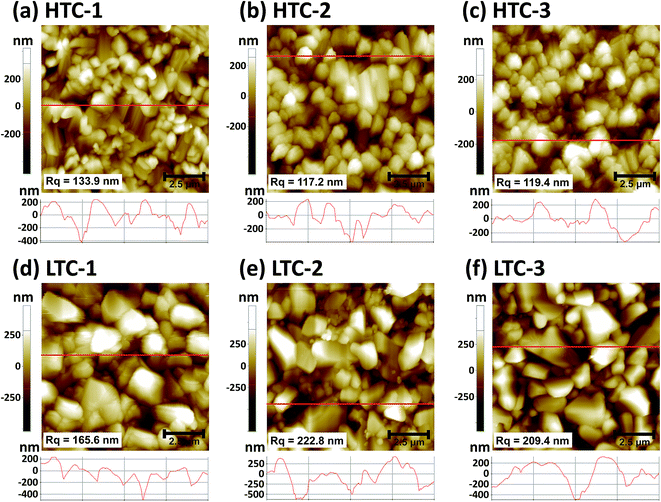 | ||
| Fig. 3 AFM images and cross-sectional height profiles of the (a) HTC-1, (b) HTC-2, (c) HTC-3, (d) LTC-1, (e) LTC-2, and (f) LTC-3 CZTSSe absorber samples. | ||
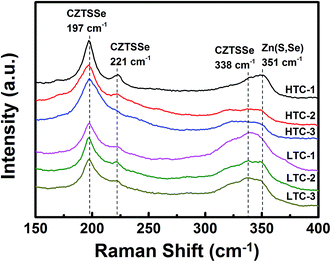
To determine the presence of secondary phases in the CZTSSe absorber surface, Raman measurements were performed at room temperature using a laser at an excitation wavelength of 514 nm. The results of the Raman measurements for the CZTSSe thin films are shown in Fig. 4. Both types of the CZTSSe absorber layers fabricated under HTC or LTC annealing conditions showed three dominant CZTSSe peaks in their Raman spectra (CZTSe-like: 197 and 221 cm−1, CZTS-like: 338 cm−1), which corresponded to the results of other studies.19,20 In addition, a peak was evident at 351 cm−1 (known as the Zn(S,Se) peak21,22), but due to the insensitivity of Zn(S,Se) to visible light, this peak could not be distinguished clearly from the CZTS-like peak at 338 cm−1.23
The HTC solar cells achieved up to 9.72% PCE whereas the LTC solar cells attained a relatively low PCE of 8.41% (Table 1). The difference between the device performances was attributed more to the FF rather than JSC or VOC since the FF might have been affected by the shunting paths detected in the SEM and AFM measurements. The LTC samples with the shunting paths attained a relatively low RSH of 217 Ω cm2 whereas the HTC samples without them achieved high RSH up to 413 Ω cm2. A PCE histogram and the means and standard deviations used to verify the statistical distributions of the HTC and LTC solar cells can be found in Fig. S2.†
| Cell | Zn/Sn ratio | PCE (%) | J SC, J–V (mA cm−2) | V OC (V) | FF (%) | R SH (Ω cm2) | R S (Ω cm2) |
|---|---|---|---|---|---|---|---|
| a The active area of each cell was 0.19 cm2. | |||||||
| CZTSSe HTC-1 | 1.07 | 8.24 | 34.3 | 0.434 | 55.4 | 209 | 2.91 |
| CZTSSe HTC-2 | 1.22 | 9.72 | 32.4 | 0.471 | 63.8 | 413 | 2.06 |
| CZTSSe HTC-3 | 1.28 | 9.30 | 34.4 | 0.469 | 57.6 | 176 | 2.80 |
| CZTSSe LTC-1 | 1.05 | 6.79 | 34.8 | 0.429 | 45.6 | 81 | 4.55 |
| CZTSSe LTC-2 | 1.27 | 7.76 | 32.7 | 0.464 | 51.2 | 151 | 4.17 |
| CZTSSe LTC-3 | 1.47 | 8.41 | 34.6 | 0.489 | 49.7 | 217 | 5.01 |
The results of the EQE measurements and the bandgap estimation are shown in Fig. 5a and b, respectively. In the 600–1000 nm wavelength region, the solar cells fabricated under LTC annealing conditions (LTC-1 and LTC-3) showed a slightly higher EQE than that of the HTC solar cells. This is in good agreement with the short circuit current (JSC) values of the CZTSSe solar cells reported in Table 1 where the JSC value of the LTC solar cells was slightly higher than that of the HTC solar cells. In addition, the bandgap energies of the six solar cells estimated to be 1.14–1.16 eV showed similar values. The JSC values of the CZTSSe solar cells were also calculated using EQE curves, the results of which are available in Table 2. The built-in potential of photovoltaic devices is known to be the major driving force for the separation of carriers, and in order to estimate it in the CZTSSe solar cells, capacitance–voltage measurements were conducted, the results of which are shown in Fig. 5c and reported in Table 2. Empirically, high performance cells have a built-in potential similar to VOC, and other studies have shown the same tendency.24–26
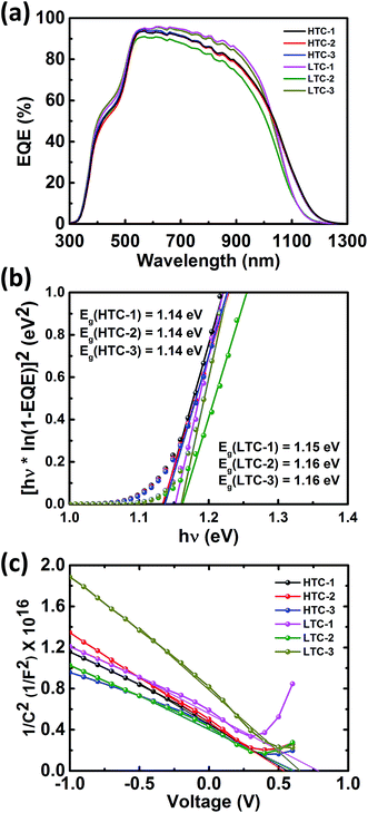 | ||
| Fig. 5 (a) External quantum efficiency curve of the CZTSSe solar cells, (b) the bandgap of the CZTSSe absorber obtained from EQE data, and (c) 1/C2vs. V plot obtained from C–V measurements. | ||
| Cell | J SC, EQE (mA cm−2) | |JSC, J–V − JSC, EQE| | E g (eV) | E g/q − VOC (V) | V bi (V) |
|---|---|---|---|---|---|
| CZTSSe HTC-1 | 32.8 | 1.5 | 1.14 | 0.706 | 0.587 |
| CZTSSe HTC-2 | 32.5 | 0.1 | 1.14 | 0.669 | 0.567 |
| CZTSSe HTC-3 | 32.9 | 1.5 | 1.14 | 0.671 | 0.606 |
| CZTSSe LTC-1 | 34.0 | 0.8 | 1.15 | 0.721 | 0.771 |
| CZTSSe LTC-2 | 31.0 | 1.7 | 1.16 | 0.696 | 0.604 |
| CZTSSe LTC-3 | 33.7 | 0.9 | 1.16 | 0.671 | 0.652 |
The laser penetration depth of the Raman measurement is known to be around 100 nm, so the deeper part of the CZTSSe solar cells required further measurement in order to detect any secondary phases.27 Therefore, HAADF STEM and EDX mapping analyses were conducted on the HTC-2 and LTC-2 samples (Fig. 6). Note that Mo and S are known to be difficult to distinguish in EDX analyses due to the overlapping energy peak;28 thus the S signal detected in the bottom is the Mo substrate of the CZTSSe solar cells. Cu was detected in the middle near the Mo layer in the case of the LTC-2 sample, which is unlike the HTC-2 sample. The excess Cu might have formed copper sulfide/selenide (CuS/Se or Cu2S/Se) secondary phases, which would have limited the performance of the solar cells.29 In other mapping data, there was no discernible difference between the HTC-2 and LTC-2 samples. The Mo(S,Se)2 layer in the LTC sample was thicker than that of the HTC sample, the details of which are shown in Fig. S3.† Increasing the thickness of Mo(S,Se)2 in the LTC sample might have increased the series resistance (RS) and decreased the FF. In addition, as can be seen in Fig. S3,† both HTC and LTC solar cells had thicker Mo(S,Se)2 layers due to the long annealing time compared to that of the reported highly efficient CZTSSe cells. However, Shin et al. explained that the c-axis of MoSe2 is parallel to the Mo surface, which improves the adhesion between CZTSe and the Mo layers.30 Therefore, it is necessary to decrease the thickness of the Mo(S,Se)2 without completely eliminating it to reduce the series resistance.
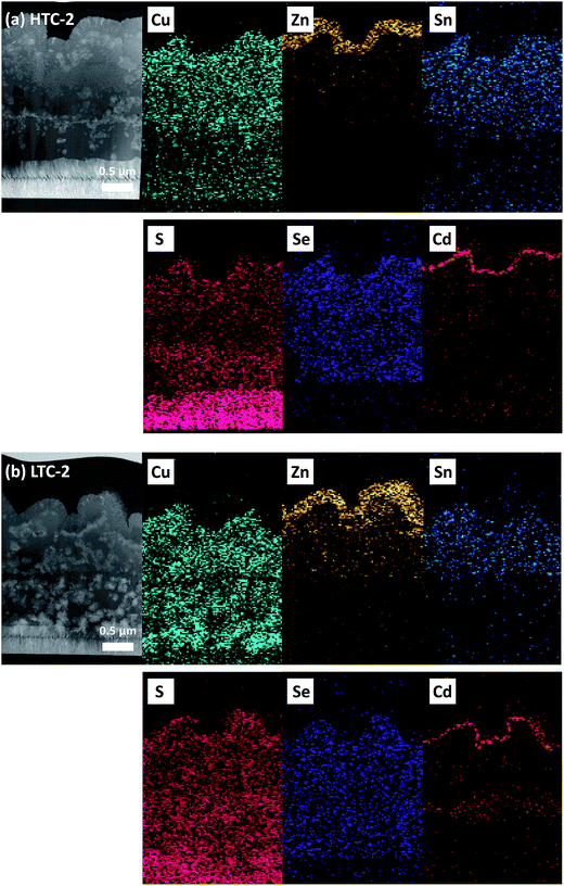 | ||
| Fig. 6 HAADF STEM image and the corresponding EDX mapping images of the CZTSSe solar cells fabricated with the (a) CZTSSe HTC-2 absorber and (b) CZTSSe LTC-2 absorber. | ||
The results of the cross-sectional SEM analysis and J–V characteristics of the best performing solar cell in this study are shown in Fig. 7. The thickness of the CZTSSe absorber layer was about 2 μm, which was similar to that of CZTSSe solar cells with over 10% efficiency.31,32 A CZTSSe solar cell with 9.716% efficiency was obtained under HTC annealing conditions with a composition ratio of Zn/Sn = 1.22. The best performing CZTSSe solar cell was certified by the Korea Institute of Energy Research (KIER), an accredited laboratory (see Fig. S4†).
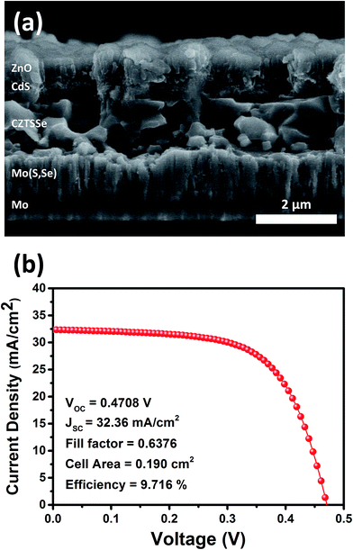 | ||
| Fig. 7 (a) Cross-sectional SEM image and (b) J–V characteristics of the best performing CZTSSe solar cell (CZTSSe HTC-2). The cell was certified by the Korea Institute of Energy Research (KIER). | ||
4. Conclusions
We quantified the effective thermal conductivity of CZTSSe absorber layers and analyzed their effects on the performance of CZTSSe solar cells. The cooling rate constants of the HTC and LTC graphite boxes used for the annealing process were found to be 1.477 × 10⁻² s−1 and 1.084 × 10⁻² s−1, respectively. The LTC samples showed a surface roughness of 199.3 ± 33.7 nm, while that of the HTC samples was 123.5 ± 10.4 nm. The LTC samples with high surface roughness also had deep valleys that decreased the shunt resistance. In addition, under LTC annealing conditions, secondary phases such as CuS and CuSe, which can act as shunting paths, were detected via HAADF STEM and EDX analyses. As a result, the LTC samples showed a lower shunt resistance of 217 Ω cm2 while that of the HTC samples was higher at up to 413 Ω cm2. We obtained a PCE of 9.72% from the CZTSSe HTC-2 solar cell sample, which was certified by an external laboratory, KIER (VOC: 0.471 V, JSC: 32.4 mA cm−2, and FF: 63.8%). This study contains essential information on highly efficient CZTSSe solar cells fabricated with earth-abundant, non-toxic, and cost-effective materials, while also demonstrating their potential.Conflicts of interest
There are no conflicts to declare.Acknowledgements
This work was supported by the GIST Research Institute (GRI) in 2018.References
- M. A. Green, Y. Hishikawa, W. Warta, E. D. Dunlop, D. H. Levi, J. Hohl-Ebinger and A. W. H. Ho-Baillie, Prog. Photovoltaics, 2017, 25, 668–676 Search PubMed.
- K. Yoshikawa, H. Kawasaki, W. Yoshida, T. Irie, K. Konishi, K. Nakano, T. Uto, D. Adachi, M. Kanematsu and H. Uzu, Nat. Energy, 2017, 2, 17032 CrossRef CAS.
- B. M. Kayes, H. Nie, R. Twist, S. G. Spruytte, F. Reinhardt, I. C. Kizilyalli and G. S. Higashi, 37th IEEE Photovoltaic Specialists Conference, Seattle, WA, June 2011 Search PubMed.
- T. Kato, A. Handa, T. Yagioka, T. Matsuura, K. Yamamoto, S. Higashi, J.-L. Wu, K. F. Tai, H. Hiroi, T. Yoshiyama, T. Sakai and H. Sugimoto, IEEE J. Photovolt., 2017, 7, 1773–1780 CrossRef.
- W. Wang, M. T. Winkler, O. Gunawan, T. Gokmen, T. K. Todorov, Y. Zhu and D. B. Mitzi, Adv. Energy Mater., 2014, 4, 1301465 CrossRef.
- S. Giraldo, T. Thersleff, G. Larramona, M. Neuschitzer, P. Pistor, K. Leifer, A. Pérez-Rodríguez, C. Moisan, G. Dennler and E. Saucedo, Prog. Photovoltaics, 2016, 24, 1359–1367 CAS.
- J. Kim, S. Park, S. Ryu, J. Oh and B. Shin, Prog. Photovoltaics, 2017, 25, 308–317 CAS.
- J. Li, H. Wang, M. Luo, J. Tang, C. Chen, W. Liu, F. Liu, Y. Sun, J. Han and Y. Zhang, Sol. Energy Mater. Sol. Cells, 2016, 149, 242–249 CrossRef CAS.
- M. G. Gang, S. W. Shin, C. W. Hong, K. V. Gurav, J. Gwak, J. H. Yun, J. Y. Lee and J. H. Kim, Green Chem., 2016, 18, 700–711 RSC.
- W.-L. Jeong, J.-H. Min, H.-S. Kim, I.-Y. Kim, J.-H. Kim and D.-S. Lee, Thin Solid Films, 2017, 638, 305–311 CrossRef CAS.
- K.-J. Yang, D.-H. Son, S.-J. Sung, J.-H. Sim, Y.-I. Kim, S.-N. Park, D.-H. Jeon, J. Kim, D.-K. Hwang, C.-W. Jeon, D. Nam, H. Cheong, J.-K. Kang and D.-H. Kim, J. Mater. Chem. A, 2016, 4, 10151–10158 CAS.
- H. R. Jung, S. W. Shin, K. V. Gurav, M. P. Suryawanshi, C. W. Hong, H. S. Yang, J. Y. Lee, J. H. Moon and J. H. Kim, Ceram. Int., 2015, 41, 13006–13011 CrossRef CAS.
- C. W. Hong, S. W. Shin, K. V. Gurav, S. A. Vanalakar, S. J. Yeo, H. S. Yang, J. H. Yun and J. H. Kim, Appl. Surf. Sci., 2015, 334, 180–184 CrossRef CAS.
- A. Fairbrother, X. Fontané, V. Izquierdo-Roca, M. Espíndola-Rodríguez, S. López-Marino, M. Placidi, L. Calvo-Barrio, A. Pérez-Rodríguez and E. Saucedo, Sol. Energy Mater. Sol. Cells, 2013, 112, 97–105 CrossRef CAS.
- L. E. Valle Rios, K. Neldner, G. Gurieva and S. Schorr, J. Alloys Compd., 2016, 657, 408–413 CrossRef CAS.
- W. Xiao, J. N. Wang, X. S. Zhao, J. W. Wang, G. J. Huang, L. Cheng, L. J. Jiang and L. G. Wang, Sol. Energy, 2015, 116, 125–132 CrossRef CAS.
- M. Placidi, M. Espindola-Rodriguez, S. Lopez-Marino, Y. Sanchez, S. Giraldo, L. Acebo, M. Neuschitzer, X. Alcobé, A. Pérez-Rodríguez and E. Saucedo, J. Alloys Compd., 2016, 675, 158–162 CrossRef CAS.
- S. N. Park, S. J. Sung, J. H. Sim, K. J. Yang, D. K. Hwang, J. Kim, G. Y. Kim, W. Jo, D. H. Kim and J. K. Kang, Nanoscale, 2015, 7, 11182–11189 RSC.
- G. Altamura, M. Wang and K. L. Choy, Sci. Rep., 2016, 6, 22109 CrossRef CAS PubMed.
- Y. Zhang, T. Yoshihara and A. Yamada, Appl. Phys. Express, 2012, 5, 012301 CrossRef.
- P. A. Fernandes, P. M. P. Salomé and A. F. da Cunha, Thin Solid Films, 2009, 517, 2519–2523 CrossRef CAS.
- K. Muska, M. Kauk-Kuusik, M. Grossberg, M. Altosaar, M. Pilvet, T. Varema, K. Timmo, O. Volobujeva and A. Mere, Thin Solid Films, 2013, 535, 35–38 CrossRef CAS.
- Z. Guan, W. Luo and Z. Zou, CrystEngComm, 2014, 16, 2929–2936 RSC.
- Y. Qu, G. Zoppi and N. S. Beattie, Prog. Photovoltaics, 2016, 24, 836–845 CAS.
- S. Pradhan, A. Stavrinadis, S. Gupta and G. Konstantatos, ACS Appl. Mater. Interfaces, 2017, 9, 27390–27395 CAS.
- H. Cui, C.-Y. Lee, W. Li, X. Liu, X. Wen and X. Hao, Int. J. Photoenergy, 2015, 2015, 1–9 CrossRef.
- M. Dimitrievska, A. Fairbrother, A. Pérez-Rodríguez, E. Saucedo and V. Izquierdo-Roca, Acta Mater., 2014, 70, 272–280 CrossRef CAS.
- M. I. Khalil, O. Atici, A. Lucotti, S. Binetti, A. Le Donne and L. Magagnin, Appl. Surf. Sci., 2016, 379, 91–97 CrossRef CAS.
- K.-H. Kim and I. Amal, Electron. Mater. Lett., 2011, 7, 225–230 CrossRef CAS.
- B. Shin, Y. Zhu, N. A. Bojarczuk, S. Jay Chey and S. Guha, Appl. Phys. Lett., 2012, 101, 053903 CrossRef.
- J. Li, S. Kim, D. Nam, X. Liu, J. Kim, H. Cheong, W. Liu, H. Li, Y. Sun and Y. Zhang, Sol. Energy Mater. Sol. Cells, 2017, 159, 447–455 CrossRef CAS.
- S. Giraldo, M. Neuschitzer, T. Thersleff, S. López-Marino, Y. Sánchez, H. Xie, M. Colina, M. Placidi, P. Pistor, V. Izquierdo-Roca, K. Leifer, A. Pérez-Rodríguez and E. Saucedo, Adv. Energy Mater., 2015, 5, 1501070 CrossRef.
Footnotes |
| † Electronic supplementary information (ESI) available: EDX spectra of the CZTSSe absorber layers, PCE histogram, cross-sectional SEM image and PCE certificate. See DOI: 10.1039/c7se00617a |
| ‡ These authors contributed equally to this work. |
| This journal is © The Royal Society of Chemistry 2018 |


