
Dark electrical bias effects on moisture-induced degradation in inverted lead halide perovskite solar cells measured by using advanced chemical probes†
Jérémy
Barbé
 a,
Vikas
Kumar
b,
Michael J.
Newman
a,
Harrison K. H.
Lee
a,
Sagar M.
Jain
a,
Hu
Chen
c,
Cécile
Charbonneau
a,
Cornelia
Rodenburg
b and
Wing C.
Tsoi
*a
a,
Vikas
Kumar
b,
Michael J.
Newman
a,
Harrison K. H.
Lee
a,
Sagar M.
Jain
a,
Hu
Chen
c,
Cécile
Charbonneau
a,
Cornelia
Rodenburg
b and
Wing C.
Tsoi
*a
aSPECIFIC, College of Engineering, Swansea University, Bay Campus, Fabian Way, Swansea, SA1 8EN, UK. E-mail: W.C.Tsoi@Swansea.ac.uk
bDepartment of Materials Science and Engineering, University of Sheffield, Mappin Street, Sheffield S1 3JD, UK
cKAUST Solar Center, Physical Science and Engineering Division, King Abdullah University of Science and Technology, Thuwal 23955-6900, Saudi Arabia
First published on 12th February 2018
Abstract
Emerging lead halide perovskite materials have enormous potential for application in a range of optoelectronic devices, such as solar cells, light emitting diodes, transistors and lasers. However, the large-scale commercialization of these technologies will depend on the ability of the active material to be stable under environmental and operating conditions. In this work, we measured for the first time the electrical bias-induced degradation of inverted perovskite solar cells in the dark in different environments and concluded that humidity coupled with electrical bias results in fast degradation of CH3NH3PbI3 into PbI2. Micro-Raman and photoluminescence show that the degradation starts from the edge of the cell due to moisture ingress. By using novel local Raman-transient photocurrent measurements, we were able to probe local ion migration in the degraded region and non-degraded region and found that the formation of PbI2 can passivate the perovskite by reducing ion migration. The degradation is far from uniform across different grains as revealed by secondary electron hyperspectral imaging, an advanced scanning electron microscopy technique which allows probing the composition of individual grains from the cross section. By using potential step chronoamperometry, we also found that the bias degradation is closely related to the density of mobile ions. The unique combination of established methods with several novel analytical tools provides an insight into the origin of the bias-degradation of inverted perovskite solar cells from the nano-scale to the cell level, and demonstrates the potential of these novel tools for studying the degradation in other perovskite systems.
1 Introduction
Since their invention in 2009,1 organometal halide perovskite solar cells (PSCs) have shown unprecedented performance improvements, now exceeding 22% power conversion efficiency.2 Beyond their performance, perovskites are the subject of intense research interest due to their potential for easier and lower-cost manufacturing than the market-leading silicon solar technology. However, ensuring the long-term stability of perovskite solar cells remains a challenge for the commercialization of this technology. Perovskite solar cells tend to degrade prematurely depending on the film quality and atmospheric conditions. Humidity,3–5 light,6 oxygen,7 temperature8 and more recently electrical stress9,10 have been shown to play an important role in initiating degradation pathways. Among them, electrical stress in the “dark” has been very rarely investigated despite being a critical parameter for solar cells. Besides, perovskites are also being considered for other optoelectronic devices such as field-effect light emitting diodes (LEDs),11 transistors12 or lasers,13 which also operate under an external bias. In particular, LEDs have an architecture and film thickness similar to those of solar devices but a relatively high turn-on voltage of 3–4 V. This implies that perovskites should be stable under a high electric field to achieve maximum external quantum efficiency and luminance.14,15Various mechanisms have been proposed to explain the degradation of the perovskite phase and resulting device performance upon applying an electric field in the dark. Using a laterally contacted device, it was suggested that methylammonium cations are loosely bound in the hydrated perovskite phase formed in the presence of moisture.10 These cations drift and accumulate near the negative electrode under the effect of an electric field, which leads to the irreversible structural modification of the depleted perovskite into PbI2 near the positive electrode. Ion migration was also observed by temperature-dependent dark current decay in a standard (top-anode) perovskite device architecture.9 The device stability was found to strongly depend on the level of applied voltage in the dark. Irreversible degradation was observed when Vapplied > Voc. This was explained by the inversion of the space charge region at the electron transport layer (ETL) interface after the displacement of a high density of ionic defects (ions or ion vacancies). Unlike these observations, D. Bryant and co-workers showed that the rapid electrical bias-induced degradation of CH3NH3PbI3 in a standard device architecture can be attributed to the diffusion of oxygen in the perovskite lattice and the formation of highly reactive superoxide species O2− when electrons are not extracted efficiently from the active layer.16 In this case, slower degradation was observed when devices were exposed to moisture alone. Hence a crucial question is to ascertain which mechanism is responsible for the degradation of PSCs under applied bias in the “dark” and to clearly establish the role played by superoxide or/and ionic defect migration.
In this work, we prepared inverted PSCs using NiOx as the HTL and investigated the effect of electrical bias in the “dark” on the device performances and material properties. The NiOx hole transport layer was chosen in this study because of its higher efficiency and reproducibility than more commonly used PEDOT:PSS. Moreover, in the course of this study, we also investigated typical PEDOT:PSS and organic small molecules as alternative HTLs and observed similar degradation, which tends to show that the degradation can be quite general. To the best of our knowledge, a study on the bias degradation of inverted PSCs in the dark is “missing” although they have several advantages over standard top-anode devices such as less hysteresis and lower processing temperatures, while obtaining record efficiencies comparable to those of the standard architecture. Besides, important questions remain for the dark bias degradation such as: what is the chemical origin of such degradation? How does the device degrade structurally? Here, we provide some insights into these questions together with new and advanced structural probes.
2 Methods
2.1 Materials
All materials were used without purification. Anhydrous dimethyl sulfoxide (DMSO), N,N-dimethylformamide (DMF), anhydrous ethanol, anhydrous chlorobenzene, anhydrous ethanolamine, anhydrous 2-methoxyethanol, bathocuproine (BCP, 96%), nickel acetate (Ni-acc, 98%) and lead iodide (PbI2, 99%) were purchased from Sigma-Aldrich. Methylammonium iodide (MAI) was purchased from Dyesol. The electron transport material [6,6]-phenyl-C61 butyric acid methyl ester (PCBM) was obtained from Solenne BV. To prepare the NiOx solution, 0.2 M solution of nickel acetate tetrahydrate was dissolved in a 1![[thin space (1/6-em)]](https://www.rsc.org/images/entities/char_2009.gif) :0.012 volume ratio of 2-methoxyethanol:ethanolamine and stirred for 1 h at 60 °C. CH3NH3PbI3 precursor solution was prepared by mixing CH3NH3I and PbI2 (1:1.05 molar ratio) in DMF/DMSO (4:1 volume ratio) with a concentration of 804 mg mL−1 at 60 °C for 2 h. PCBM was dissolved in chlorobenzene with a concentration of 20 mg mL−1 and stirred overnight at 60 °C. BCP was dissolved in anhydrous ethanol with a concentration of 0.5 mg mL−1. All solutions were filtered with 0.45 μm PTFE syringe filters.
:0.012 volume ratio of 2-methoxyethanol:ethanolamine and stirred for 1 h at 60 °C. CH3NH3PbI3 precursor solution was prepared by mixing CH3NH3I and PbI2 (1:1.05 molar ratio) in DMF/DMSO (4:1 volume ratio) with a concentration of 804 mg mL−1 at 60 °C for 2 h. PCBM was dissolved in chlorobenzene with a concentration of 20 mg mL−1 and stirred overnight at 60 °C. BCP was dissolved in anhydrous ethanol with a concentration of 0.5 mg mL−1. All solutions were filtered with 0.45 μm PTFE syringe filters.
2.2 Perovskite solar cell fabrication and testing
15 Ω □−1 ITO/glass substrates (Lumtec) were sequentially cleaned with detergent in DI water, acetone, and isopropyl alcohol in an ultrasonic bath. Subsequently, they were dried with N2 and exposed to O2 plasma for 10 min. A 20 nm-thick NiOx layer was deposited via spin-coating at 4000 rpm for 30 s followed by 30 min sintering at 250 °C. Subsequent layers were prepared under nitrogen in a glovebox. The perovskite precursor solution was spin coated at 4000 rpm for 30 s. Chlorobenzene was drop-cast onto the rotating sample after 15 s of spinning to promote crystallization. The 400 nm perovskite film was annealed at 100 °C for 10 min. After cooling, the PCBM solution was spin-coated onto the CH3NH3PbI3 layer at 4000 rpm for 30 s, followed by spin-coating the BCP solution at 6000 rpm for 20 s. The thickness of the PCBM is 60 nm. The thickness of the BCP film is too thin to be measured by profilometry or SEM. Finally, 100 nm thick silver counter electrodes were evaporated at 10−4 Torr using an Edwards 306 thermal evaporator, forming devices with an active area of 0.15 cm2.Current density–voltage (J–V) characterizations were determined by using a Keithley 2400 source-meter unit under 0.8 sun illumination using a Newport 92193A-1000 solar simulator. Current–voltage sweeps were performed from both VOC-to-JSC and vice versa at a rate of 0.1 V s−1.
2.3 Material characterization
Raman and photoluminescence measurements were performed with a Renishaw inVia Raman system in a backscattering configuration. A 532 nm laser and 50× objective were used (NA: 0.50, spot size ≈ 1 μm). For single point Raman measurements, a laser power of 0.6 mW and an acquisition time of 30 s were used; for the Raman and PL line mapping, 0.6 mW/5 s and 0.06 μW/1 s laser power/acquisition time were used for each measurement point, respectively. 1800 gr per mm and 300 gr per mm gratings were used for Raman and photoluminescence, respectively. Local photocurrent measurements were acquired using the laser beam and X–Y scanning stage from the Raman system (Renishaw inVia, 532 nm, 50× objective) and a Keithley 236 source-meter unit. The devices were measured under nitrogen using a Linkam atmospheric chamber. The solar cell was held at short-circuit in the dark until the residual current dropped below 5 nA (which can take up to 60 s). Then, the laser shutter was open and the photocurrent was monitored over time. A low laser power of 0.3 mW was used to avoid any further degradation of the perovskite film by the laser beam during the measurement.XRD measurements were carried out using a Bruker D8 Discover instrument with a CuKα beam (wavelength is 0.15418 nm) at 40 kV and 40 mA, and scan parameters of 1 s per step at a 2θ step size of 0.03°.
The basic principles of the experimental method to collect hyperspectral images (SEHI) have been reported by P. Kazemian et al.17 In this work, we used an FEI Helios NanoLab G3 UC SEM. All the samples are imaged using a through-lens detector (TLD) at a working distance of 4.0 mm with a beam current of 6.3 pA and an accelerating voltage of 1 kV. The required hyperspectral window was selected (0–6.0 eV) by setting the mirror electrode to 0 V. For all SEHI images, the dwell time was adjusted to 50 ns.
Chronoamperometry measurements were carried out using a Keithley 236 source-meter unit controlled by software. The dark current through the cell was continuously recorded during the applied voltage sequence: the cell was first left at short-circuit for 30 s to allow equilibrium to be reached. Then, a forward bias of 1 V was applied for 30 s before the device was switched to short-circuit mode (0 V) for 30 s (until the current stabilized to a few nanoamperes). The device was switched on and off successively several times. The same procedure was also carried out at 0.5 V and 0.85 V.
The total charge density was estimated from the current transients under short-circuit conditions by integrating the current decay as described below:
 | (1) |
3 Results and discussion
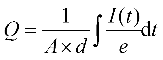
We first investigated the effect of electrical bias in the dark coupled with water vapor and/or oxygen on the PSC performance. PSCs with the structure glass/ITO/NiOx/CH3NH3PbI3(MAPI)/PC60BM/BCP/Ag were fabricated and subjected to 1 V forward bias in air (40% RH), dry N2, dry air and humid N2. All degradations in this work were performed in the dark. In the case of humid N2, a water-saturated atmosphere (≈100% humidity) was obtained by flowing N2 through a sealed water jar. The current–voltage (J–V) curves before and after bias applications are shown in Fig. 1a. When exposed to air or humid N2, the cell drastically degraded after 1 h bias application mostly due to a large drop in Jsc. When exposed to dry N2 or dry air, the biased cells only suffered minor degradation characterized by a slight drop of the Jsc, but no change in FF or Voc. These results demonstrate the key role played by water vapor in the degradation of PSCs under bias in the dark, whereas oxygen does not have a significant effect. Even in scenarios where devices were degraded in dry N2 or dry air, the slight loss in efficiency (from 10.4% to 8.8% and 10.7% to 8.8%, respectively) may be attributed to the presence of small amounts of water (or any polar molecules as explained by Leijtens et al.10) in the perovskite stack, due to the sample being exposed to the ambient atmosphere prior to conducting the degradation tests, or perhaps while in contact with polar solvents in the glovebox during device fabrication. Oxygen and the formation of superoxides, although suggested by others16 as another important path towards the degradation of lead halide perovskite materials, do not appear to have a significant effect in this case (dark, dry environment, 1 V). It was shown that oxygen molecules enter the perovskite at a fast rate and uniformly saturate perovskite vacancies after only a few seconds.18 As we purged the atmospheric chamber for 10 min before measurement with a relatively high flow rate of dry air, it is reasonable to assume that samples exposed to this environment were saturated with oxygen when the bias was applied. The fact that the device was relatively stable under dry air (the same trend as in dry N2) diminishes the role of highly reactive superoxide species, at least during the first hour of degradation.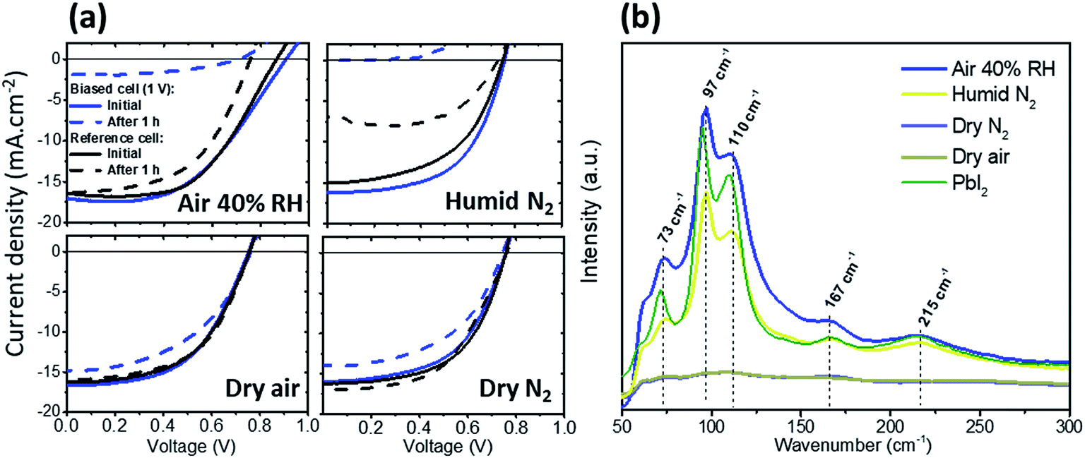 | ||
| Fig. 1 (a) Current density–voltage curves of perovskite devices at 0.8 sun before (solid blue lines) and after (dashed blue lines) biasing at 1 V for 1 h under dark conditions in different atmospheres. Reference cells left in the same environment for the same duration but without bias are also shown for comparison (black lines). (b) Corresponding Raman spectra for the biased cells and reference PbI2 film (intensity reduced by 10 times for comparison). | ||
Fig. 1b shows the Raman spectra for the four different cells after degradation. The cells degraded in 40% RH air and humid N2 reveal the features of PbI2, with a main peak at 97 cm−1 associated with the stretching mode of Pb–I19 (the higher intensity measured for 40% RH is due to local inhomogeneities but does not reflect the degradation level), and other characteristic peaks at 75 cm−1, 110 cm−1, 167 cm−1 and 215 cm−1. This indicates that a large fraction of the MAPI converted to PbI2 when exposed to 40% RH air or humid N2 under 1 V bias. In the case of devices exposed to dry air or dry N2, the Raman data confirm a very small amount of PbI2, thus correlating device performance results.
Numerous reports showed that metal contacts play an important role in the degradation of perovskite devices. In particular, it has been observed that in the presence of moisture, Ag can be converted to AgI due to the migration of I− ions and Ag through pinholes in the Spiro-OMeTAD layer in the standard architecture.20 However, we didn't observe any XRD diffraction peaks due to AgI (peaks at 2θ = 22.3°, 23.8°, and 39.2° for β-AgI)21 when measuring the bias degraded cell (1 V, 1 h, humid N2) through the Ag top electrode (Fig. S1a,† blue curve). This suggests that such a degradation mechanism is not likely to happen in the inverted perovskite device structure and can be explained by the fundamental difference that unlike the standard device structure, a positive bias is applied to the ITO and not to the Ag electrode for the inverted device structure (so negative ions will be attracted to the ITO).The only difference between the XRD spectra of the degraded and non-degraded cells is the appearance of the PbI2 peak at 12.6° after degradation, which agrees well with the Raman results.
To confirm the role of moisture in the degradation of PSCs, freshly prepared samples were exposed to a humid N2 environment for 20 min without bias. This procedure allowed water molecules to penetrate into the perovskite film, in particular where the stack is not covered by the Ag top electrode or near the edges of the electrode. After this preconditioning, a bias was applied in air for short times, and optical microscopy images of the cell edge were recorded at different intervals (Fig. S2†). No visual degradation is observed up to 70 s at 1 V bias, before exposure to humid N2. However, following exposure to humidity, the application of a bias clearly triggers the appearance of degradation features after only a few seconds. These are particularly concentrated near the long edge of the cell while the center of the cell and short edges are much better preserved. In this paper, the “long” edges are defined by the silver top electrode, while the “short” edges are defined by the ITO stripe, as shown in Fig. 2d. Similar patterns were observed when the cell is exposed to air with 40% RH and biased for 20 min, as shown in Fig. 2a. These observations were further correlated with Raman and photoluminescence intensity profiles acquired across 300 μm from outside the edge of a cell toward the center, as shown in Fig. 2b and c. The results show that the cell is highly degraded across 130 μm, starting from the edge of the cell. This is supported by the 3-fold increase of the PbI2 Raman peak at 96 cm−1 and more than 10 times drop in PL intensity at 775 nm.
 | ||
| Fig. 2 (a) Optical microscope image of the “long” edge of the degraded perovskite cell after 20 min under 1 V bias in humid air. (b) PbI2 Raman intensity profiles measured at 96 cm−1 along the edge. (c) Photoluminescence peak intensity profile at 775 nm. (d) Optical image showing the ITO and Ag electrodes delimitating the cells measured in this work. The “long” and “short” edges of the cells are shown as red and blue lines, respectively. | ||
The degradation pattern could be explained as follows: the 100 nm-thick silver top electrode acts as a barrier for water vapor and protects, to some extent, the underlying perovskite film. However, moisture ingress is much stronger at the long edges of the cell where the silver electrode finishes. As water penetrates into the device stack from the long edge of the cell, hydrated phases of the perovskite are formed (as shown by several reports3,4,22), which then rapidly converts to PbI2 under the effect of the electric field (Fig. S1†). In comparison, when the cell was not previously hydrated, the bias-induced degradation occurs in minutes instead of seconds because of the much lower density of water molecules present in the MAPI film (Fig. 2). We also observed that the short edges were much less degraded than the long edges. Indeed, the short edges are delimited by the ITO bottom electrode while the Ag electrode continues further away, thus better protecting the short edges from environmental conditions.
XRD measurements were also carried out to investigate the formation of hydrated phases of the perovskite when exposed to a humid environment. For this purpose, a sample was measured by focusing an X-ray beam outside the Ag electrode, to directly probe the perovskite/PCBM/BCP film after exposure to a high humidity environment (1 h, 100% RH in N2). For repeated measurements on different samples, most of the time no diffraction peaks due to monohydrate CH3NH3PbI3:H2O or dihydrate (CH3NH3)4PbI6:2H2O were observed.3 However, these metastable intermediate phases are usually difficult to measure because they are time and space-limited. Even recent in situ synchrotron XRD measurements in a high humidity environment could detect hydrated phases only from time to time during the degradation process.22 Thus, the fact that we couldn't easily detect such a phase doesn't mean that monohydrate or dihydrate perovskite is not formed when moisture penetrates into the film, especially as the samples were measured at least 15 min after high humidity exposure and could have dried in the meantime depending on the atmospheric conditions (Leguy et al. showed that hydrated perovskite crystals can dry in less than 15 min when exposed to dry air).3 Note that, occasionally, we observed a new peak at 37.9°, which has a similar position to the XRD peak of (CH3NH3)4PbI6:2H2O (Fig. S1b,† orange curve).3 This tends to suggest that hydrated perovskite phases form in the film, although they are momentary and dependent on the atmospheric conditions.
At this stage, the results demonstrate that the combined effects of water molecule ingress and applied bias are responsible for the degradation of the perovskite film to PbI2. Next, making use of the various degradation levels that are formed at the cell edge after biasing, we performed localized photoelectrical characterization by focusing the laser beam of the Raman system (1 μm diameter) at the center (region 1) or at the edge (region 2) of the cell, as represented in Fig. 3a. The Raman spectra shown in Fig. 3b confirm that two distinct levels of degradation are obtained: for region 1, the CH3NH3PbI3 phase was well preserved, showing two broad peaks at 250 cm−1 and 110 cm−1, which can be assigned to the methylammonium cation torsional and libration modes, respectively.23 For region 2, significantly more PbI2 (at 96 cm−1 and 110 cm−1) relative to CH3NH3PbI3 is generated. Although a clear Raman signal from CH3NH3PbI3 at 250 cm−1 was not observed for region 2, it does not necessary mean that all perovskite degraded to form PbI2, as the Raman cross section of the perovskite is much lower than that of PbI2 and thus can be masked by the much stronger PbI2 signal.19 This is further supported by the significant amount of photocurrent generated in region 2 although PbI2 absorbs very little (if any) light at the laser excitation wavelength, as explained in the next paragraph.
 | ||
| Fig. 3 (a) Optical microscope image of the degraded cell with the 2 different regions (edge and inner side of the cell) used for local characterization (b–d). (b) Micro-Raman spectra. (c) Local photocurrent stabilization curves measured at short-circuit (laser excitation power 0.3 mW). (d) Normalized photocurrent stabilization curves. | ||
Photocurrent stabilization curves for the two different regions are shown in Fig. 3c and d. To ensure that all measurements were started under the same equilibrium conditions, the solar cell was held at short-circuit in the dark until the residual current dropped below 5 nA (which can take up to 60 s). Then, the laser shutter was opened and the photocurrent was monitored over time. A low laser power of 0.3 mW was used to avoid any further degradation of the perovskite film by the laser beam during the measurement.19 In the non-degraded region (region 1), the photocurrent quickly switches to −2.7 μA but then gradually rises to reach −4.8 μA after 80 s. In contrast, in the highly degraded region (region 2), the photocurrent quickly reaches a stabilized value of −1.4 μA without long transients. The long photocurrent transient can be explained by ion migration according to several recent studies.9,24,25 The photovoltage induces mobile ions to slowly move in the perovskite layer and to screen the electric field until ions reach a new equilibrium. This slow motion of mobile ions (and vacancies) is observed by the rise of the photocurrent toward a steady-state value at short-circuit upon turning on the illumination. Alternatively, Shao et al. explained the slow photocurrent transient by a trap filling process at grain boundaries and the perovskite surface.26
The results shown in Fig. 3b and d indicate that when a large amount of PbI2 is formed, the photocurrent transient is suppressed: the photocurrent quickly switches to a stabilized value, similarly to crystalline silicon solar cells which don't have ionic conductivity.9 The two different rising times for the photocurrent measured in regions 1 and 2 are more clearly observed in the normalized curves in Fig. 3d. Since PbI2 has very low absorption at 532 nm,19 it is likely that the photocurrent measured in region 2 is generated in the residual perovskite which was masked in the Raman spectra by the large amount of PbI2 formed. These results are in good agreement with recent reports showing that incorporating some excess PbI2 into CH3NH3PbI3 solution27 or forming a PbI2 secondary phase in the CH3NH3PbI3 film through post-deposition thermal annealing25 can significantly reduce J–V hysteresis by suppressing ion migration. Obviously, the amount of PbI2 formed at the edge of the cell is much too high to improve the device performance in our case but the results indicate that ion migration can be suppressed or highly reduced in the residual perovskite as a large amount of PbI2 is formed. Hence, the local Raman-photoelectrical characterization of perovskite solar cells gives direct physical insights into the correlation between the local degradation (amount of PbI2) and local electronic-ionic processes with micrometer resolution. To our knowledge, the information obtained by this novel technique cannot be obtained by other approaches.
Next, to better understand the effect of applied bias on the degradation of the perovskite layer in the presence of moisture, secondary electron hyperspectral cross-sectional images were acquired for a cell biased at 1 V in 40% RH air for 1 h and compared to those of a reference cell (no bias). Secondary electron hyperspectral imaging (SEHI) is an advanced imaging technique making use of differences in the secondary electron spectra of materials in a SEM to characterize local variations in the composition and electronic structure of materials with sub-10 nm resolution.28 The hyperspectral images in Fig. 4 show uniform contrast across the reference sample (Fig. 4a), but clear contrast variations in the case of the degraded sample: some grains appear brighter than other grains (Fig. 4b). This suggests a modification of the chemical composition of these grains, consistent with the hypothesis of ion migration. Interestingly, the contrast variation indicates that the degradation is not uniform at the sub-micrometer scale and varies when comparing individual grains. We suggest that the degradation ability of each crystalline grain under bias depends on the initial structural quality and composition of the grain. Indeed, the concentration of mobile defects in individual grains can be affected by the processing conditions which often lead to local non-uniformity.29 Here, based on the clear contrast variations observed between crystalline grains from the same perovskite film, we may conclude that the application of an electrical bias is responsible for the drift of variable concentrations of ionic defects within each grain, resulting in distinct levels of highly localized degradation. At this stage of development of the technique (SEHI), it is not possible to measure the precise composition of the degraded grains. However, the Raman (and XRD) results suggest that these grains are composed of a large amount of PbI2. The fact that both degraded and non-degraded grains sit next to each other at the microscopic scale in the highly degraded perovskite confirms that residual non-degraded perovskite remains in the degraded cell, which correlates well with the local photoelectrical characterization (Fig. 3c and d).
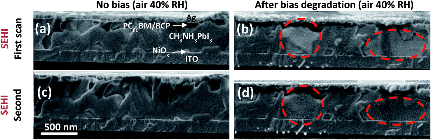 | ||
| Fig. 4 Cross-sectional hyperspectral secondary electron images (SEHI) in the range of 0–6.0 eV before (a) and after (b) bias-induced degradation in 40% RH air (1 V for 1 h). (c) and (d) SEHI of the same devices and areas after a second scan. | ||
Further evidence of the localized level of degradation of individual grains is provided by comparing Fig. 4b and d, illustrating two consecutive secondary electron hyperspectral images of the same cross-sectional area of the biased sample in the energy range of 0–6 eV (additional images provided in ESI Fig. S3†). In Fig. 4d, 20–30 nm size dots were found to appear at the surface of bright degraded grains (red circles, magnified image in Fig. S4†), but not at the surface of darker grains. This is in agreement with other studies showing that even moderate e-beam currents (86 pA) and acceleration voltages (10 kV) can induce an aggressive and very localized degradation of perovskite films due to ion migration.30,31 In comparison, the reference sample did not show the appearance of e-beam induced nano-scale dots (Fig. 4c). These results confirm that the composition of some specific crystalline grains was modified by biasing the device in humid air, and thus became even more sensitive to further degradation by the e-beam. We note that SEHI could be a fast and efficient novel method to investigate the chemical changes due to degradation in individual grains inside the film, which is particularly interesting for PSCs.
To further understand the complementary roles of ion migration and humidity in the bias-induced degradation of perovskite devices, solid-state stepped chronoamperometry measurements were carried out. At this stage, the question is: can we correlate the degradation of the device performance under electrical bias with the density of mobile ionic defects in the perovskite, and how is it related to the presence of moisture?
In Fig. S5,† dark current measurements for square wave voltage with various peak voltages show the “discharging” behavior below Voc and “charging” behavior above Voc until a steady state is reached after a few seconds. These transient behaviors have been previously explained by the movement of ions in the perovskite layer which screen the electric field for seconds as the dynamic response of ions is much slower than that of electrons and holes.9,32 If mechanisms other than ion migration may affect the current response, such as ferroelectric polarization or trapping of electrons at the interfaces, the rate of these mechanisms would be likely to be fast33,34 relative to the slow timescales of current responses shown in Fig. S5.†
The transient response of the dark current to a potential step has been used to estimate the density of mobile ions present in perovskite devices. In Fig. S6,† square wave potential steps between 0 and 1 V were applied to the device while the dark current was monitored. The shape of the dark current curve can be explained similarly to the transistor-type device used by D. Li et al.:35 when a positive bias (1 V) is applied to the device, a current is immediately measured due to the drift of electronic carriers in the device. The bias then induces mobile ions to gradually move toward the contacts until equilibrium is reached after a few seconds when the ion-induced electric field cancels the applied bias in the perovskite bulk, which is observed by the stabilization of the dark current. After removing the applied bias (0 V), the previously accumulated ions at the perovskite–electrode interfaces create a net reversal electric field, leading to an instant switching of the polarity of the electronic current. The accumulated ions gradually diffuse away from the perovskite–electrode interfaces, resulting in the decrease of the ion-induced electric field and thus the reduction of the dark electronic current. Hence, it is quite clear that there is interplay between the ionic and electronic current. The origin of electronic carriers in the dark can be explained by the buildup of an electrostatic potential at the interfaces due to the band bending induced by ion accumulation, as explained by R. Gottesman et al.36 When the bias is switched off, the electrostatic potential at the interface remains for a few seconds before the device is “discharged” when mobile ions reached a new equilibrium.
From this picture, we see that the magnitude of the ion-induced electric potential (or the number of displaced mobile ions) will affect the magnitude and time constant of the measured dark current. By integrating the area below the electronic current decay, we can thus estimate an “integrated charge density” which is proportional to the number of ions displaced in the device (mobile ion density). This measurement is similar to a recent study by S. Bae et al.9 except that the dark current is integrated after the voltage is removed.
Two cells from the same sample were measured shortly after fabrication and after storage in air (40% RH) for two days (Fig. 5). For the fresh cell, the integrated charge density is 2 × 1018 cm−3 at 0.5 V bias and increases up to 1.2 × 1019 cm−3 at 1 V. For the aged cell, the charge density is similar at 0.5 V bias (3 × 1018 cm−3) but considerably increases with higher voltage, up to 7.2 × 1019 cm−3 at 1 V, which is 6 times higher than that of the fresh cell. As the sample was exposed to air without encapsulation, environmental moisture entered the perovskite film and likely formed a hydrated phase containing more loosely bound ions.10 At 0.5 V forward bias, the electric field is too low to activate these ions, which remain fixed in the crystalline structure. Thus, similar charge density is measured for the fresh and aged cells. However, at 0.85 V or 1 V the electric field is then sufficient to activate loosely bound ions and allow them to migrate in the hydrated perovskite (aged cell), which explains the significant increase in charge density. These results can be correlated with the degradation of the performance of the fresh and aged cells under dark bias. In Fig. S7b,† it is observed that the fresh cell degrades in hours instead of minutes for the aged cell, meaning that the perovskite devices having higher density of mobile ionic defects degrade faster under applied bias.
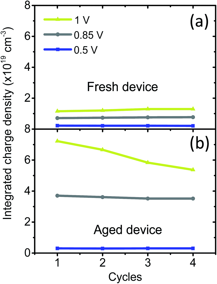 | ||
| Fig. 5 Integrated charge density (proportional to mobile ionic defect density) estimated from the integration of the transient part of the dark current under short-circuit conditions just after biasing at 0.5 V, 0.85 V and 1 V for (a) a fresh perovskite device and (b) a device aged in air for two days. | ||
In addition, for the aged cell it can be observed that the charge density slowly decreases from 7.2 × 1018 cm−3 after the first potential step at 1 V to 5.4 × 1018 cm−3 after 4 potential steps. This trend can be explained as follows:9 as mobile ions move to the opposite interface under the effect of an electrical bias, they may be trapped if the space charge region at this interface is inverted, which occurs if the applied voltage is greater than Voc or if a large number of ions are displaced. As these ions are trapped, they cannot flow back in the perovskite bulk when the cell is switched back to short-circuit and do not participate in the measured current decay, which explains the charge density decrease at 1 V observed for the aged cell. This is not true for the fresh cell which has a higher Voc of 1 V (current–voltage curves under 1 sun for the fresh and aged cells are shown in Fig. S7a†), i.e. similar to the applied bias, and lower charge density. In this case, the opposite interface is depleted but not inverted and mobile ions are less likely to be trapped. Indeed, the charge density remains unchanged even after four potential steps at 1 V.
Finally, the electrical bias stability of triple-cation mixed-halide perovskites was examined as they are known to have better moisture stability than conventional methylammonium lead halide perovskites.37,38 For this purpose, Cs0.1(MA0.17FA0.83)0.9Pb(I0.83Br0.17)3 perovskite solution was prepared following a recipe described in another study39 and used as an absorber layer in devices with the same architecture and interlayers as described above. The final device gave a maximum efficiency of 11.6%, which is closed to the state-of-the-art performance for triple-cation perovskites processed on top of NiOx.40 Then, the dark bias stability of the device was measured by applying 1 V forward bias for 1 h in 40% RH air. The J–V curves before and after aging are shown in Fig. S9† and compared to those of a reference cell (without bias). The performances of the biased and non-biased cells are similar after aging, which indicates that the electrical bias has little or no effect on degradation for this kind of cell. This is ascribed to the better stability of Cs0.1(MA0.17FA0.83)0.9Pb(I0.83Br0.17)3 perovskite to moisture. By avoiding the formation of a hydrated phase when exposed to moisture, the triple-cation mixed-halide perovskite device is insensitive to the applied bias, which is in contrast to CH3NH3PbI3 cells which suffer from strong degradation under the same aging conditions (Fig. 1a). This is consistent with previous results showing that moisture can enhance ionic mobility in CH3NH3PbI3, which will eventually have a detrimental and irreversible effect on the stability of the cells when an external bias is applied. Multiple-cation mixed-halide perovskites could be an efficient alternative for improving the moisture and electrical bias stability of perovskite solar cells.
4 Conclusions
In summary, we showed that humidity is the main factor responsible for the bias-induced degradation of inverted devices based on CH3NH3PbI3 perovskite in the dark, as degradation due to oxygen (superoxide) is not observed. Besides, XRD does not show any AgI, which implies that degradation related to the Ag electrode is likely to be mild (if any), which is different to the standard device structure, and can be explained by the fundamental difference that a positive bias is applied to the ITO in the inverted device structure (which attracts I− to the ITO side). Our results suggest that, as the perovskite solar cell is exposed to a humid environment, moisture penetrates into the film preferentially from the edges of the cell and likely forms a hydrated perovskite phase which contains a high density of loosely bound ions. Under the effect of an external electric field, mobile ionic defects drift in the perovskite, which results in the accelerated degradation of the active layer and eventually irreversible conversion of CH3NH3PbI3 into PbI2. A novel Raman-transient photoelectrical technique is developed which allows probing local photoelectrical properties in highly degraded and non-degraded regions. It indicates that the presence of a large amount of PbI2 suppresses or strongly reduces the migration of ionic species in the residual perovskite. By applying an advanced cross-sectional hyperspectral secondary electron imaging technique, inhomogeneous degradation of distinct crystal grains was observed at the nano-scale which could be explained by variations in the structural quality and ionic defect density from grain to grain. Our study provides significant insight into the bias degradation of inverted perovskite solar cells in the dark. Importantly, the new techniques developed and applied here should be powerful to study the degradation of perovskite solar cells and other optoelectronic devices in general.Conflicts of interest
There are no conflicts to declare.Acknowledgements
The authors acknowledge funding from the EPSRC (grant no. EP/M025020/1 & EP/N008065/1), the Welsh Assembly Government funded Sêr Cymru Solar Project, and the European Union's Horizon 2020 research and innovation programme under the Marie Skłodowska-Curie grant agreement no. 663830. They thank Dr Joel Troughton and Dr Trystan Watson for advice on device fabrication and Dr Adam Pocket for discussions on device physics and ion migration.References
- A. Kojima, K. Teshima, Y. Shirai and T. Miyasaka, Organometal Halide Perovskites as Visible-Light Sensitizers for Photovoltaic Cells, J. Am. Chem. Soc., 2009, 131(17), 6050–6051 CrossRef CAS PubMed.
- W. S. Yang, B.-W. Park, E. H. Jung, N. J. Jeon, Y. C. Kim, D. U. Lee, S. S. Shin, J. Seo, E. K. Kim, J. H. Noh and S. Seok, Il. Iodide Management in Formamidinium-Lead-Halide Based Perovskite Layers for Efficient Solar Cells, Science, 2017, 356(6345), 1376–1379 CrossRef CAS PubMed.
- M. A. Leguy, Y. Hu, M. Campoy-quiles, M. I. Alonso, O. J. Weber, P. Azarhoosh, M. van Schilfgaarde, M. T. Weller, T. Bein, J. Nelson, P. Docampo and P. R. F. Barnes, Reversible Hydration of CH3NH3PbI3 in Films, Single Crystals, and Solar Cells, Chem. Mater., 2015, 27, 3397–3407 CrossRef.
- J. Yang, B. D. Siempelkamp, D. Liu and T. L. Kelly, Investigation of CH3NH3PbI3 Degradation Rates and Mechanisms in Controlled Humidity Environments Using in Situ Techniques, ACS Nano, 2015, 9(2), 1955–1963 CrossRef CAS PubMed.
- J. A. Christians, P. A. Miranda Herrera and P. V. Kamat, Transformation of the Excited State and Photovoltaic Efficiency of CH3NH3PbI3 Perovskite upon Controlled Exposure to Humidified Air, J. Am. Chem. Soc., 2015, 137(4), 1530–1538 CrossRef CAS PubMed.
- T. Leijtens, G. E. Eperon, S. Pathak, A. Abate, M. M. Lee and H. J. Snaith, Overcoming Ultraviolet Light Instability of Sensitized TiO2 with Meso-Superstructured Organometal Tri-Halide Perovskite Solar Cells, Nat. Commun., 2013, 4, 2885 Search PubMed.
- A. J. Pearson, G. E. Eperon, P. E. Hopkinson, S. N. Habisreutinger, J. T. W. Wang, H. J. Snaith and N. C. Greenham, Oxygen Degradation in Mesoporous Al2O3/CH3NH3PbI3−xClx Perovskite Solar Cells: Kinetics and Mechanisms, Adv. Energy Mater., 2016, 1–10 Search PubMed.
- B. Conings, J. Drijkoningen, N. Gauquelin, A. Babayigit, J. D'Haen, L. D'Olieslaeger, A. Ethirajan, J. Verbeeck, J. Manca, E. Mosconi, F. De Angelis and H. G. Boyen, Intrinsic Thermal Instability of Methylammonium Lead Trihalide Perovskite, Adv. Energy Mater., 2015, 5(15), 1–8 Search PubMed.
- S. Bae, S. Kim, S. W. Lee, K. J. Cho, S. Park, S. Lee, Y. Kang, H. S. Lee and D. Kim, Electric-Field-Induced Degradation of Methylammonium Lead Iodide Perovskite Solar Cells, J. Phys. Chem. Lett., 2016, 7(16), 3091–3096 CrossRef CAS PubMed.
- T. Leijtens, E. T. Hoke, G. Grancini, D. J. Slotcavage, G. E. Eperon, J. M. Ball, M. De Bastiani, A. R. Bowring, N. Martino, K. Wojciechowski, M. D. McGehee, H. J. Snaith and A. Petrozza, Mapping Electric Field-Induced Switchable Poling and Structural Degradation in Hybrid Lead Halide Perovskite Thin Films, Adv. Energy Mater., 2015, 5(20), 1–11 Search PubMed.
- N. Wang, L. Cheng, R. Ge, S. Zhang, Y. Miao, W. Zou, C. Yi, Y. Sun, Y. Cao, R. Yang, Y. Wei, Q. Guo, Y. Ke, M. Yu, Y. Jin, Y. Liu, Q. Ding, D. Di, L. Yang, G. Xing, H. Tian, C. Jin, F. Gao, R. H. Friend, J. Wang and W. Huang, Perovskite Light-Emitting Diodes Based on Solution-Processed Self-Organized Multiple Quantum Wells, Nat. Photonics, 2016, 10(11), 699–704 CrossRef CAS.
- T. Yajima, Y. Hikita and H. Y. Hwang, A Heteroepitaxial Perovskite Metal-Base Transistor, Nat. Mater., 2011, 10(3), 198–201 CrossRef CAS PubMed.
- H. Zhu, Y. Fu, F. Meng, X. Wu, Z. Gong, Q. Ding, M. V. Gustafsson, M. T. Trinh, S. Jin and X.-Y. Zhu, Lead Halide Perovskite Nanowire Lasers with Low Lasing Thresholds and High Quality Factors, Nat. Mater., 2015, 14(6), 636–642 CrossRef CAS PubMed.
- L. Zhao, J. Gao, Y. L. Lin, Y.-W. Yeh, K. M. Lee, N. Yao, Y.-L. Loo and B. P. Rand, Electrical Stress Influences the Efficiency of CH3NH3PbI3 Perovskite Light Emitting Devices, Adv. Mater., 2017, 1605317, 1605317 CrossRef PubMed.
- S. Myoung and H. Song, High-Performance Perovskite Light-Emitting Diodes via Morphological Control of Perovskite Film, Nanoscale, 2016, 8, 7036–7042 RSC.
- D. Bryant, N. Aristidou, S. Pont, I. Sanchez-Molina, T. Chotchunangatchaval, S. Wheeler, J. R. Durrant and S. A. Haque, Light and Oxygen Induced Degradation Limits the Operational Stability of Methylammonium Lead Triiodide Perovskite Solar Cells, Energy Environ. Sci., 2016, 9, 1655 CAS.
- P. Kazemian, S. A. M. Mentink, C. Rodenburg and C. J. Humphreys, Quantitative Secondary Electron Energy Filtering in a Scanning Electron Microscope and Its Applications, Ultramicroscopy, 2007, 107(2–3), 140–150 CrossRef CAS PubMed.
- N. Aristidou, C. Eames, I. Sanchez-molina, X. Bu, J. Kosco, M. S. Islam and S. A. Haque, Fast Oxygen Diffusion and Iodide Defects Mediate Oxygen-Induced Degradation of Perovskite Solar Cells, Nat. Commun., 2017, 8, 1–10 CrossRef PubMed.
- K. E. A. Hooper, H. K. H. Lee, M. J. Newman, S. Meroni, J. Baker, T. M. Watson and W. C. Tsoi, Probing the Degradation and Homogeneity of Embedded Perovskite Semiconducting Layers in Photovoltaic Devices by Raman Spectroscopy, Phys. Chem. Chem. Phys., 2017, 19, 5246–5253 RSC.
- T. Zhang, X. Meng, Y. Bai, S. Xiao, C. Hu, Y. Yang, H. Chen and S. Yang, Profiling the Organic Cation-Dependent Degradation of Organolead Halide Perovskite Solar Cells, J. Mater. Chem. A, 2017, 5(3), 1103–1111 CAS.
- Y. Kato, L. K. Ono, M. V. Lee, S. Wang, S. R. Raga and Y. Qi, Silver Iodide Formation in Methyl Ammonium Lead Iodide Perovskite Solar Cells with Silver Top Electrodes, Adv. Mater. Interfaces, 2015, 2(13), 2–7 Search PubMed.
- J. Zhao, B. Cai, Z. Luo, Y. Dong, Y. Zhang, H. Xu, B. Hong, Y. Yang, L. Li, W. Zhang and C. Gao, Investigation of the Hydrolysis of Perovskite Organometallic Halide CH3NH3PbI3 in Humidity Environment, Sci. Rep., 2016, 6(1), 21976 CrossRef CAS PubMed.
- C. Quarti, G. Grancini, E. Mosconi, P. Bruno, J. M. Ball, M. M. Lee, H. J. Snaith, A. Petrozza and F. Angelis, De. The Raman Spectrum of the CH3NH3PbI3 Hybrid Perovskite: Interplay of Theory and Experiment, J. Phys. Chem. Lett., 2014, 5, 279–284 CrossRef CAS PubMed.
- C. Eames, J. M. Frost, P. R. F. Barnes, B. C. O'Regan, A. Walsh and M. S. Islam, Ionic Transport in Hybrid Lead Iodide Perovskite Solar Cells, Nat. Commun., 2015, 6(May), 7497 CrossRef CAS PubMed.
- T. Du, C. Burgess, J. Kim, J. Durrant, J. Zhang and M. McLachlan, Formation, Location and Beneficial Role of PbI2 in Lead Halide Perovskite Solar Cells. Sustain, Energy Fuels, 2017, 119–126 CAS.
- Y. Shao, Z. Xiao, C. Bi, Y. Yuan and J. Huang, Origin and Elimination of Photocurrent Hysteresis by Fullerene Passivation in CH3NH3PbI3 Planar Heterojunction Solar Cells, Nat. Commun., 2014, 5, 1–7 Search PubMed.
- Y. C. Kim, N. J. Jeon, J. H. Noh, W. S. Yang, J. Seo, J. S. Yun, A. Ho-Baillie, S. Huang, M. A. Green, J. Seidel, T. K. Ahn and S. Seok, Il. Beneficial Effects of PbI2 Incorporated in Organo-Lead Halide Perovskite Solar Cells, Adv. Energy Mater., 2016, 6(4), 1502104 CrossRef.
- V. Kumar, W. L. Schmidt, G. Schileo, R. C. Masters, M. Wong-stringer, D. C. Sinclair, I. M. Reaney, D. Lidzey and C. Rodenburg, Nanoscale Mapping of Bromide Segregation on the Cross Sections of Complex Hybrid Perovskite Photovoltaic Films Using Secondary Electron Hyperspectral Imaging in a Scanning Electron Microscope, ACS Omega, 2017, 2, 2126–2133 CrossRef CAS.
- M. Okano, M. Endo, A. Wakamiya, M. Yoshita, H. Akiyama and Y. Kanemitsu, Degradation Mechanism of Perovskite CH3NH3PbI3 Diode Devices Studied by Electroluminescence and Photoluminescence Imaging Spectroscopy, Appl. Phys. Express, 2015, 8, 102302 CrossRef.
- H. Yuan, E. Debroye, K. Janssen, H. Naiki, C. Steuwe, G. Lu, M. Moris, E. Orgiu, H. Uji-I, F. De Schryver, P. Samorì, J. Hofkens and M. Roeffaers, Degradation of Methylammonium Lead Iodide Perovskite Structures through Light and Electron Beam Driven Ion Migration, J. Phys. Chem. Lett., 2016, 7(3), 561–566 CrossRef CAS PubMed.
- O. Hentz, Z. Zhao and S. Gradečak, Impacts of Ion Segregation on Local Optical Properties in Mixed Halide Perovskite Films, Nano Lett., 2016, 16(2), 1485–1490 CrossRef CAS PubMed.
- S. E. J. O'Kane, G. Richardson, A. Pockett, R. G. Niemann, J. M. Cave, N. Sakai, G. E. Eperon, H. J. Snaith, J. M. Foster, P. J. Cameron and A. B. Walker, Measurement and Modelling of Dark Current Decay Transients in Perovskite Solar Cells, J. Mater. Chem. C, 2017, 5(2), 452–462 RSC.
- P. Calado, A. M. Telford, D. Bryant, X. Li, J. Nelson, B. C. O'Regan and P. R. F. Barnes, Evidence for Ion Migration in Hybrid Perovskite Solar Cells with Minimal Hysteresis, Nat. Commun., 2016, 7, 1–10 Search PubMed.
- S. Meloni, T. Moehl, W. Tress, M. Franckevicius, M. Saliba, Y. H. Lee, P. Gao, M. K. Nazeeruddin, S. M. Zakeeruddin, U. Rothlisberger and M. Graetzel, Nat. Commun., 2016, 7, 10334 CrossRef CAS PubMed.
- D. Li, H. Wu, H. C. Cheng, G. Wang, Y. Huang and X. Duan, Electronic and Ionic Transport Dynamics in Organolead Halide Perovskites, ACS Nano, 2016, 10(7), 6933–6941 CrossRef CAS PubMed.
- R. Gottesman, P. Lopez-Varo, L. Gouda, J. A. Jimenez-Tejada, J. Hu, S. Tirosh, A. Zaban and J. Bisquert, Dynamic Phenomena at Perovskite/Electron-Selective Contact Interface as Interpreted from Photovoltage Decays, Chem, 2016, 1(5), 776–789 CAS.
- J. H. Noh, S. H. Im, J. H. Heo, T. N. Mandal and S. Seok, Il. Chemical Management for Colorful, Efficient, and Stable Inorganic-Organic Hybrid Nanostructured Solar Cells, Nano Lett., 2013, 13(4), 1764–1769 CrossRef CAS PubMed.
- Z. Li, M. Yang, J. S. Park, S. H. Wei, J. J. Berry and K. Zhu, Stabilizing Perovskite Structures by Tuning Tolerance Factor: Formation of Formamidinium and Cesium Lead Iodide Solid-State Alloys, Chem. Mater., 2016, 28(1), 284–292 CrossRef CAS.
- M. Saliba, T. Matsui, J.-Y. Seo, K. Domanski, J.-P. Correa-Baena, M. K. Nazeeruddin, S. M. Zakeeruddin, W. Tress, A. Abate, A. Hagfeldt and M. Grätzel, Cesium-Containing Triple Cation Perovskite Solar Cells: Improved Stability, Reproducibility and High Efficiency, Energy Environ. Sci., 2016, 9(6), 1989–1997 CAS.
- S. Weber, T. Rath, J. Mangalam, B. Kunert, A. M. Coclite, M. Bauch, T. Dimopoulos and G. Trimmel, Investigation of NiOx-Hole Transport Layers in Triple Cation Perovskite Solar Cells, J. Mater. Sci.: Mater. Electron., 2017, 0(0), 1–9 Search PubMed.
Footnote |
| † Electronic supplementary information (ESI) available. See DOI: 10.1039/c7se00545h |
| This journal is © The Royal Society of Chemistry 2018 |