Creation of oxygen vacancies to activate WO3 for higher efficiency dye-sensitized solar cells†
Received
5th October 2017
, Accepted 16th November 2017
First published on 16th November 2017
Abstract
In this work, oxygen vacancies were created to activate tungsten trioxide (WO3) as a highly efficient counter electrode (CE) in dye-sensitized solar cells (DSSCs). The levels of oxygen vacancies (OVs) in WO3 were finely formed and tuned by doping with different weight percentages (3, 5, and 9 wt%) of urea and annealing in a N2 environment at 470 °C. The urea doped WO3 significantly improved the electrocatalytic behaviour in the iodide–triiodide electrolyte. The effects of OVs on the catalytic performance of WO3 CEs were fully studied and understood. This improvement was attributed to the introduction of OVs into WO3, which acted as surface shallow states to facilitate electron transfer from the WO3 counter electrode to the electrolyte. At a high temperature of 470 °C, urea decomposes into the reactive H2 gas that can remove oxygen atoms from the WO3 surface and create OVs. 5 wt% urea was found to be the optimal urea concentration that led to the highest catalytic performance as evidenced by the cyclic voltammetry measurements. The 5 wt% urea doped WO3 CE-based device achieved a power conversion efficiency (PCE) of ∼10.5%, which was improved from the reference Pt CE-based device at ∼9.3% and non-active WO3 CE based cell at 3.32%. This has led to the optimal number of OVs that facilitate the charge transfer at the CE/electrolyte interface.
1. Introduction
Dye-sensitized solar cells (DSSCs) were widely reported over the last several decades because of their low cost, ease of fabrication, and relatively high-power conversion efficiency (PCE).1–4 Efficiency up to 13% was achieved using porphyrin sensitizers and cobalt redox electrolyte.5 DSSCs are typically fabricated using mesoporous metal oxides such as TiO2 sensitized by N719-dye as the photoanode, triiodide/iodide (I3−/I−) redox electrolyte, and platinum-counter electrode (CE). Counter electrodes have a significant impact on the overall efficiency of DSSCs. Platinum is the most commonly used counter electrode in DSSCs due to the excellent electrocatalytic performance towards redox electrolytes. However, the low-abundance and high-cost of platinum hinder the large-scale commercialization opportunity of DSSCs.6–8 As alternatives, many other materials were reported as low-cost counter electrodes. Carbon-based nanostructures,8,9 conductive polymers,10 metal-based sulfides,11,12 carbides,13 nitrides,14 selenides15 and composites16 have been reported to replace the platinum counter electrode. Also, low-cost, abundant transition metal oxides have been reported as counter electrodes in DSSCs17–20 to replace the high-cost platinum-based electrode. However, their electrocatalytic performance is outperformed by that of the standard platinized-electrodes.21 The introduction of oxygen vacancies as shallow surface states in metal oxides was found to improve the charge transfer and conductivity.22,23 The applications of using oxygen-deficient metal oxides are vast in Li-ion and lithium–air batteries where oxygen-deficient metal oxides showed enhanced catalytic performance and stability in comparison with the commercial pristine metal oxides.24–26 Other applications of oxygen-deficient metal oxides are that they can be used as effective photo-catalysts in the water splitting industry for both H2 and O2 generation. Also, oxygen-deficient metal oxides were found to have lower band gaps compared to pristine metal oxides, which allow absorbing more light in the visible region and hence higher photocatalytic performance.27–29 The oxygen vacancy concentrations can be optimized in metal oxides to improve catalyst performance. Previous reports have used metal oxides such as TiO2, SnO2, and WO3 for both photo-anodes and counter electrodes.30 This strongly depends on the annealing environment. Annealing metal oxides in H2 or N2 gases can help create shallow states (oxygen vacancies) to facilitate electron transfer from the counter electrode to the electrolyte.3,19,31,32 Song et al. used ammonia gas (NH3) as the annealing atmosphere for WO3 counter electrodes and they found better catalytic performance than those annealed in H2 or N2 gas individually.33
In this work, a novel technique was developed to create and tune the oxygen deficiency of commercial WO3 film to improve the catalytic performance of CEs in DSSCs. This technique used different concentrations (3, 5, and 9 wt%) of urea to dope WO3 films before annealing in the N2 atmosphere at 470 °C. Adding urea helped to create and tune oxygen vacancies in order to activate WO3 for higher DSSC photovoltaic performance.
2. Experimental procedures
2.1. Materials
The chemicals were used without further purification. WO3 (typically 99.9% pure, <5 μm average particle size) was purchased from CERAC, Inc., USA. Fluorine doped tin dioxide (FTO) substrates were purchased from Hartford Glasses. Mesoporous TiO2 (Ti-Nanoxide HT/SP), scattering TiO2 (Ti-Nanoxide R/SP), N719 dye (Ruthenizer 535-bisTBA), and iodide/triiodide electrolyte (Iodolyte AN 50) were ordered from Solaronix. The other materials were ordered from Sigma-Aldrich Corporation.
2.2. Counter electrode fabrication
Three different urea-pretreated WO3-based counter electrodes were fabricated by mixing 0.1 gm of pristine WO3 with various weight percentages (wt%) of urea (3, 5, and 9 wt%). Alpha-terpineol (100 μL) and ethyl cellulose (0.005 gm) were added, followed by grinding the whole mixture in a mortar for 15 min until a uniform paste was obtained. The paste was applied on a cleaned FTO substrate using the doctor-blade technique on a 0.25 cm2 mask, followed by annealing in a N2 atmosphere at 470 °C for 2 h in a tube furnace. The obtained counter electrodes, U3-WO3, U5-WO3, and U9-WO3 correspond to WO3 counter electrode doped with 3 wt%, 5 wt%, and 9 wt% of urea, respectively. For comparison, pristine WO3 (P-WO3) CE without urea doping was prepared by grinding a mixture of 0.1 gm of pristine WO3 powder in a mortar with alpha-terpineol (100 μL) and 5 mg of ethyl cellulose. The paste was applied on a cleaned FTO substrate using the doctor-blade technique on a 0.25 cm2 mask. The film was then annealed in open air at 110 °C for 1 h to get rid of any solvent residues. Also, a N2-annealed WO3 counter electrode at 470 °C without any urea pre-treatment (N-WO3) was fabricated. The reference platinum CE was prepared by spin coating 20 mM of hydrogen hexachloroplatinate(IV) hexahydrate, 99.9% (trace metal basis, Acros Organics) in ethanol at 2000 rpm for 20 s on top of the FTO substrate, followed by annealing at 400 °C for 15 min.
2.3. Photoanode fabrication and device assembly
FTO substrates were cleaned in an ultrasonic bath of detergent, deionized (DI) water, acetone, and isopropanol (IPA) for 15 min each. A dense, compact layer of TiO2 was spin coated from 0.15 M of titanium diisopropoxide bis(acetylacetonate), 75 wt% in an ethanol solution onto FTO substrates followed by annealing at 450 °C for 30 min. Then, a nanocrystalline TiO2 (Ti-Nanoxide HT/SP, Solaronix) layer was deposited twice to reach a thickness of ∼11 μm via doctor blading and sintered at 450 °C for 30 min. The TiO2 light scattering layer was prepared by doctor blading a larger particle size (>100 nm) Ti-Nanoxide R/SP, followed by sintering at 450 °C for 30 min. This layer can scatter light in the photoanode that leads to re-absorption by the dyes attached on the photoanode layer for improved light harvesting and higher short circuit current JSC generation. Then the photoanode was dip-treated using 40 mM solution of TiCl4 at 70 °C for 30 min followed by washing with ethanol and drying using compressed N2 gas. The TiCl4 treated TiO2 was then sintered at 450 °C for 30 min. The TiCl4 treatment led to the hydrolysis of titanium tetrachloride (TiCl4) to produce titanium dioxide (TiO2). This process will result in a coating of a thin layer of TiO2 to passivate any defect states in the mesoporous TiO2 active layer and suppress electron recombination. Lastly, the fabricated photoanodes were immersed in 0.3 mM N-719 dye solution in valeronitrile/acetonitrile (1![[thin space (1/6-em)]](https://www.rsc.org/images/entities/char_2009.gif) :1 by volume) for 18 h to attach dye molecules. The dye-attached photoanodes were rinsed with anhydrous acetonitrile to remove any excess of dye molecules and then dried using compressed nitrogen. Both photo-anode and CE were then assembled using a thermoplastic sealant (Meltonix, Solaronix Co.). The thermoplastic sealant was cut into a rectangular shape with the dimensions of about 2.5 cm × 1.5 cm. A circular hole with an area of 0.25 cm2 was made in the sealant using a puncher. Two narrow channels of about 1 mm width were made along the line of the diameter of the hole for injecting the electrolyte. The sealant was kept on the FTO surface in such a way that metal oxide CE films were located at the centre of the hole. The CE with the sealant was kept on a hot plate to make sure the glass side of the CE was in contact with the hot plate. The CE was heated at 80 °C, and the sealant was gently pressed with a cotton tip so that the sealant stuck to the FTO without melting the sealant. Then the photo-anode was placed on the sealant so that the dye-sensitized TiO2 film was located directly over the hole on the sealant and above the circular CE film. The assembled layers of the photo-anode, the sealant, and the CE were heated on the hot plate from the glass side of the CE at ∼110 °C for <2 min while pressing together from the glass side of the photo-anode. Once the sealant was melted by simultaneously applying heat and pressure, the cell was immediately removed from the hot plate and cooled down to room temperature. An electrolyte (Iodolyte AN-50) was injected into the cell through one of the channels made on the sealant using a plastic pipette. Once the space between the photoanode and the CE was filled with the electrolyte, the holes at each end of the channels were sealed with hot glue (Adhesive Tech, melting point of 193 °C).
:1 by volume) for 18 h to attach dye molecules. The dye-attached photoanodes were rinsed with anhydrous acetonitrile to remove any excess of dye molecules and then dried using compressed nitrogen. Both photo-anode and CE were then assembled using a thermoplastic sealant (Meltonix, Solaronix Co.). The thermoplastic sealant was cut into a rectangular shape with the dimensions of about 2.5 cm × 1.5 cm. A circular hole with an area of 0.25 cm2 was made in the sealant using a puncher. Two narrow channels of about 1 mm width were made along the line of the diameter of the hole for injecting the electrolyte. The sealant was kept on the FTO surface in such a way that metal oxide CE films were located at the centre of the hole. The CE with the sealant was kept on a hot plate to make sure the glass side of the CE was in contact with the hot plate. The CE was heated at 80 °C, and the sealant was gently pressed with a cotton tip so that the sealant stuck to the FTO without melting the sealant. Then the photo-anode was placed on the sealant so that the dye-sensitized TiO2 film was located directly over the hole on the sealant and above the circular CE film. The assembled layers of the photo-anode, the sealant, and the CE were heated on the hot plate from the glass side of the CE at ∼110 °C for <2 min while pressing together from the glass side of the photo-anode. Once the sealant was melted by simultaneously applying heat and pressure, the cell was immediately removed from the hot plate and cooled down to room temperature. An electrolyte (Iodolyte AN-50) was injected into the cell through one of the channels made on the sealant using a plastic pipette. Once the space between the photoanode and the CE was filled with the electrolyte, the holes at each end of the channels were sealed with hot glue (Adhesive Tech, melting point of 193 °C).
2.4. Thin film characterization and device evaluation
The current density–voltage (J–V) characterization of DSSCs was conducted using a xenon lamp (Newport 67005) with an AM 1.5 filter to obtain a light intensity of 100 mW cm−2. Electrochemical impedance spectroscopy (EIS), cyclic voltammetry (CV), Mott–Schottky (MSC), and Tafel polarization measurements were conducted using an Ametek VERSASTAT3-200 potentiostat with a frequency analysis module (FDA). EIS measurements were performed on dummy devices made of two identical counter electrodes assembled together with an electrolyte injected in between. A perturbation AC signal of amplitude 20 mV was applied with a frequency range 100–0.1 kHz under 0 V DC bias and dark conditions. Cyclic voltammetry (CV) measurements were conducted at a potential scan rate of 50 mV s−1 and using a three-electrode setup. Silver/silver chloride (Ag/AgCl) was used as the reference electrode, platinum wire as the counter electrode, and the fabricated CE as the working electrode. The electrolyte for CV measurements was prepared using 10 mM LiI, 0.5 mM I2 and 0.1 M tetra-n-butylammonium tetrafluoroborate in acetonitrile. The Mott–Schottky measurement was conducted with the same three electrodes and supporting electrolyte as used in CV characterization. An AC signal with an amplitude of 20 mV and a fixed frequency of 100 Hz were applied while the DC voltage bias was swept from −1 V to 1 V with an increment of 0.05 V. A Hitachi-S3400N scanning electron microscope (SEM) with an electron dispersive X-ray (EDX) setup at an applied bias of 5 kV was used for surface morphology characterization. The element wt% measurements were conducted on all fabricated metal oxide counter electrodes. Raman spectra of the fabricated CEs were recorded using a Horiba LabRam HR 800 Raman spectrometer with a laser beam of 784.32 nm (red laser) for all CEs.
3. Results and discussion
Fig. 1 shows different CEs fabricated from pristine films (P-WO3), N2-annealed films (N-WO3) and urea pretreated N2-annealed films with different urea wt% (U3-WO3, U5-WO3, U9-WO3).
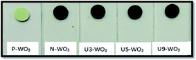 |
| | Fig. 1 Different CEs fabricated from pristine films (P-WO3), N2-annealed films (N-WO3) and urea pretreated N2-annealed films with different wt% of urea-treated metal oxides (U3-WO3, U5-WO3, and U9-WO3). | |
As shown in Fig. 1, the film colour turned from white green for pristine WO3 to dark black film after annealing in a N2 atmosphere. The film colour remains black even after urea pre-treatment with no significant colour change from non-pretreated N2-annealed WO3 films.
The surface morphology of fabricated WO3 CE films before and after urea-pretreatment with various urea wt% was measured by SEM, as shown in Fig. 2. The surface morphology of pristine WO3 CE (P-WO3) is dense and compact which is not ideal for penetration of the iodide/triiodide electrolyte. The surface morphology of N2-annealed WO3 films in a N2 environment (N-WO3) without urea pre-treatment was found to be very similar to that of the pristine sample (P-WO3) without significant change in film compactness. On the other hand, when 3 wt% of urea was used for WO3 pretreatment prior to annealing in the N2 atmosphere (U3-WO3 CE), pores were introduced in the film. More voids were introduced in the film by increasing the wt% of urea pre-treatment at 5 wt% and 9 wt% of urea. The creation of voids in the film by applying urea pre-treatment could be due to urea decomposition to ammonia at temperature ∼180 °C (ref. 34) as shown in eqn (1). Then ammonia decomposes at higher temperatures (>400 °C) into reactive H2 and inert N2 gas as shown in eqn (2).35–37
| | | H2N–CO–NH2 ↔ NH3 + HNCO | (1) |
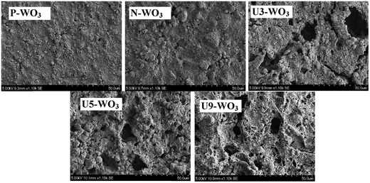 |
| | Fig. 2 SEM images for pristine WO3 (P-WO3), N2-annealed WO3 (N-WO3) and the pre-treated N2-annealed WO3 with 3 wt% (U3-WO3), 5 wt% (U5-WO3), and 9 wt% (U9-WO3) urea. | |
The reducing H2 gas helps reduce the metal oxide (WO3) at high temperatures and introduces OVs by taking oxygen atoms from metal oxides in the form of H2O vapour38,39 as shown in eqn (3). More H2 gas produced by increasing urea wt% will lead to more oxygen atom extraction from metal oxide films. This leads to more pores and voids in the metal oxide films.
| | | WO3 + H2 → H2O + WO3−x + e− | (3) |
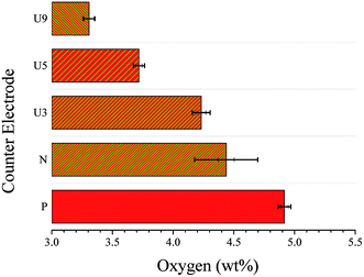
Energy dispersive X-ray spectroscopy was performed for all WO3 CE films before and after applying urea at the different wt%. This measurement was conducted to calculate the oxygen wt% in the films by increasing the urea content of the pre-treated films. Fig. 3 shows the plot of oxygen wt% for different types of metal oxide CEs. The oxygen wt% for the pristine (P-WO3) metal oxide is the highest with a value of ∼4.9% after annealing in the N2 atmosphere; the oxygen wt% in N-WO3 CE film decreased to ∼4.4%, which indicates that OVs were introduced after annealing. The oxygen wt% value was further decreased with increasing the wt% of urea. Oxygen wt% values are 4.2%, 3.7%, and 3.3% for U3-WO3, U5-WO3, and U9-WO3, respectively. The decrease in oxygen wt% by increasing urea wt% is direct evidence for the proposed hypothesis of greater oxygen loss by increasing urea content for pre-treated WO3 metal oxide films.
 |
| | Fig. 3 Oxygen wt% for pristine WO3 (P-WO3), N2-annealed WO3 (N-WO3) and the pre-treated N2-annealed WO3 with 3 wt% (U3-WO3), 5 wt% (U5-WO3), and 9 wt% (U9-WO3) urea. | |
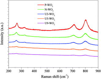
Fig. 4 shows Raman spectra of WO3 films before and after urea-pretreatment. Pristine WO3 CE film shows four main peaks at 264 cm−1, 324 cm−1, 710 cm−1 and 801 cm−1. The four peaks are attributed to the monoclinic crystal structure of WO3.40 Raman peaks become broader with lower peak intensity for N2-annealed WO3 (N-WO3), suggesting degradation of WO3 crystallinity into WO3−x due to the reduction of WO3 and OV formation. By applying urea pre-treatment and annealing in N2 gas, Raman peaks become broader and lower in intensity. The peaks become even broader by increasing the urea content until the peaks almost disappear in the case of the highest urea wt% for U9-WO3. This result is consistent with the previously reported Raman spectra of WO2.9,40 which supports the hypothesis of the increase of OVs by increasing the urea content for the pre-treated WO3 CEs.
 |
| | Fig. 4 Raman spectra of pristine WO3 (P-WO3), N2-annealed WO3 (N-WO3) and pre-treated N2-annealed WO3 with 3 wt% (U3-WO3), 5 wt% (U5-WO3), and 9 wt% (U9-WO3) urea. | |
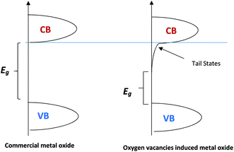
The effect of oxygen vacancies or defects at the metal oxide surface has been studied to understand the electronic and chemical behaviour in photocatalysts and gas sensors.41–55 The introduction of oxygen vacancies has been achieved using different methods and techniques such as H2 treatment, chemical reduction, chemical oxidation, and anodization–annealing.56–58 Oxygen vacancies can result in excess free electrons in the metal oxides. Therefore, metal oxides will be more electron-rich as an n-type semiconductor and the Fermi level will be negatively shifted closer to the conduction band minima (CBM) level.59,60 Another effect of oxygen vacancies is the decrease of the metal oxide band gap (Eg) due to the introduction of the extended tail states close to the conduction band, which lowers the position of conduction band minima (CBM),59,60 as shown in Fig. 5.
 |
| | Fig. 5 Diagram showing the effect of oxygen vacancies on the metal oxide band gap. | |
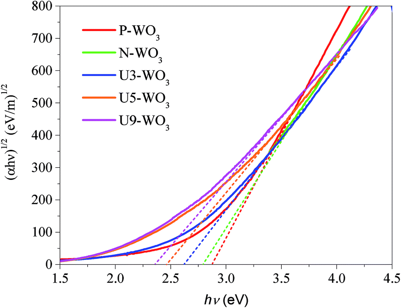
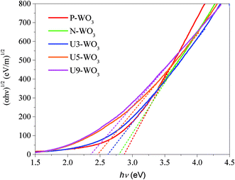
Fig. 6 shows Tauc's plots for pristine WO3 (P-WO3), N2-annealed WO3 (N-WO3), and urea pre-treated N2-annealed WO3 with various urea wt%, U3-WO3, U5-WO3, and U9-WO3. Eqn (4) is also called Tauc's equation:61–65
where
A is a constant,
hν is the photon energy,
Eg is the optical band gap,
α is the absorption coefficient, and
n is the exponential coefficient which denotes the nature of electron transition from the valence to the conduction band.
 |
| | Fig. 6 Tauc plot for pristine WO3 (P-WO3), N2-annealed WO3 (N-WO3) and the pre-treated N2-annealed WO3 with 3 wt% (U3-WO3), 5 wt% (U5-WO3), and 9 wt% (U9-WO3) urea. | |
The electronic bandgap transition is indirect for WO3 metal oxide where the exponential coefficient value (n) in eqn (4) is 2.61 The intercept of curve plots with the x-axis as shown in Fig. 5 determines the value of the optical band gap (Eg). The optical band gap value for pristine WO3 (P-WO3) was calculated at ∼2.85 eV. After annealing in N2, Eg value was reduced to ∼2.79 eV, and this decrease is attributed to the introduction of OVs inside WO3 metal oxide when annealed in a N2 atmosphere. Oxygen vacancies will result in excess electrons produced in the metal oxide. Therefore, the metal oxide will be more electron rich as an n-type semiconductor, and the Fermi level will be negatively shifted closer to the conduction band minima (CBM) level.59,60 Another effect of OVs is the decrease of the metal oxide band gap (Eg). The band gap decrease was attributed to the introduction of energy bands close to conduction band minima (CBM) and valence band maxima (VBM). The new energy states will shift the CBM level downward (positive shift) and VBM level upward due to the extended tail state formation.59,60 The optical band gap (Eg) was further decreased to ∼2.61 eV for U3-WO3 CE. More OVs mean more in-gap donor states will be formed, and as a result, the band gap will be reduced. The theory is consistent with the experimental results where the optical band gap (Eg) values of WO3 CEs were inversely proportional to urea wt%. The value of Eg was found to be ∼2.45 eV and 2.34 eV for U5-WO3 and U9-WO3 CEs, respectively.
Mott–Schottky measurements can be used to calculate defect state density and Fermi-level position change upon electrochemical reaction in semiconductors or metal oxide materials when in contact with the electrolyte. When the n-type WO3 metal oxide is in contact with the electrolyte, band bending at the electrolyte/semiconductor interface will occur due to the energy difference in Fermi level positions for both metal oxide and electrolyte. As a result, a depletion region or space charge region will form, where no charges will be located in this region but outside the depletion region. The relationship which can control this change in band bending is called the Mott–Schottky relationship as shown in eqn (5).66
| |  | (5) |
where
Vfb is the flat band potential, which is the potential needed to flatten the band bending at the counter electrode/electrolyte interface,
Csc is the space charge capacitance,
ε is the dielectric constant of the metal oxide,
εo is the permittivity of free space,
ND is the dopant density, and
VA is the applied potential
vs. the Ag/AgCl reference cell.
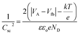
Fig. 7 shows the Mott–Schottky plot (1/Csc2vs. VA) for pristine P-WO3, N2-annealed N-WO3, and different wt% urea pre-treated N2-annealed CEs. The plots intercept with the x-axis and give the values of Vfb. For pristine P-WO3 CEs, the value of Vfb was −0.326 (vs. Ag/AgCl). For N2 annealed non-pretreated N-WO3 CEs, the Vfb value was positively increased to −0.227 (vs. Ag/AgCl). The positive increase in Vfb value is attributed to the decrease in the potential difference between the Fermi-level of N-WO3 CE and the redox potential of the electrolyte. This decrease is caused by the introduction of OVs, which leads to a downward shift of the CBM level of metal oxide and hence reduces the potential barrier between the Fermi-level of N-WO3 CE and redox potential of the electrolyte.60,67 The value of Vfb was further positively increased to ∼−0.084 for U3-WO3 CE, −0.01 for U5-WO3 CE, and ∼+0.053 for U9-WO3 CE. As the urea wt% increases, the number of OVs increases and hence the potential difference between the metal oxide CBM and redox potential of the electrolyte will decrease. It was noticed that U5-WO3 CE shows the lowest potential difference between its CBM level and the redox potential of the electrolyte indicated by the lowest Vfb value. Due to the band alignment of both the CBM level of U5-WO3 and redox potential of the electrolyte, electrons will be efficiently transferred through the interface between the U5-WO3 CE and electrolyte. Beyond the optimum conditions with increasing urea contents for U9-WO3, the Vfb potential increased to a positive potential. This could be attributed to that the work function of U9-WO3 CE is higher than that of the iodide/triiodide electrolyte. Therefore, the band bending will be downward at the interface after the contact formation. Thus, a positive potential is needed to flatten the band bending and again the band bending would not be favourable for efficient electron transfer at the interface between U9-WO3 CE and the electrolyte.
 |
| | Fig. 7 Mott–Schottky plots for pristine WO3 (P-WO3), N2-annealed WO3 (N-WO3) and pre-treated N2-annealed WO3 with 3 wt% (U3-WO3), 5 wt% (U5-WO3), and 9 wt% (U9-WO3) urea. | |
Fig. S1 (ESI†) shows the band structure diagrams at the interfaces of the P-WO3/iodide-triiodide electrolyte, N-WO3/iodide–triiodide electrolyte, U3-WO3/iodide–triiodide electrolyte, U5-WO3/iodide–triiodide electrolyte and U9-WO3/iodide–triiodide electrolyte. As shown in Fig. S1,† the optical band gap decreased when the urea doping wt% increased due to the formation of surface tail states near the conduction band. Along with the decrease of band gap, the upward band bending at the interface between WO3-based CE electrodes decreased by increasing the urea doping wt%. It is noticed that for U5-WO3 CE, there is almost no band bending at the interface as the flat band potential obtained from the Mott–Schottky experiment is about −0.01 eV. However, the flat-band potential value changed positive in the case of the U9-WO3 CE/electrolyte by about +0.08 eV. This could be caused by the fact that the work function of U9-WO3 is higher than that of the iodide/triiodide electrolyte before contact formation. Therefore, the band bending shifted downward as seen in Fig. S1.†
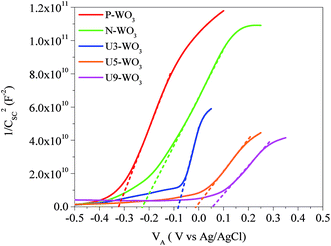
CV is a widely used technique to study electrochemical reactions. Fig. 8 shows the CV plots (current density mA cm−2vs. potential) for pristine WO3 (P-WO3), N2-annealed (N-WO3) WO3, urea pre-treated WO3 CEs with different wt% urea (U3-WO3, U5-WO3, and U9-WO3) and Pt CE. The CV curves for Pt CE showed a pair of anodic and cathodic peaks on the left side where Jpa and Jpc were assigned to anodic and cathodic peak current densities. These were attributed to the electrochemical reactions in eqn (6) and (7).
| | | I3− + 2e− → 3I−, (cathodic reaction) | (6) |
| | | 3I− → I3− + 2e−, (anodic reaction) | (7) |
 |
| | Fig. 8 Cyclic voltammetry curves for pristine WO3 (P-WO3), N2-annealed WO3 (N-WO3) and pre-treated N2-annealed WO3 with 3 wt% (U3-WO3), 5 wt% (U5-WO3), and 9 wt% (U9-WO3) urea, and Pt CE. | |
The catalytic performance of counter electrodes can be determined by these two reactions.68 The cyclic voltammetry plot showed no peaks for P-WO3 films due to the poor catalytic performance towards the redox electrolyte. By annealing WO3 films in a N2 atmosphere, one anodic peak starts to appear, but no cathodic peaks were present. However, two pairs of anodic and cathodic peaks started to show up after the urea pre-treatment. The current density values for both anodic (Jpa) and cathodic (Jpc) peaks corresponding to the reactions in eqn (4) and (5) were enhanced by increasing urea wt% pre-treatment for U3-WO3 and U5-WO3 CEs. The enhancements in anodic and cathodic currents are attributed to the increase in OVs which facilitates the reduction process of triiodide ions and hence improves the catalytic performance. The optimum catalytic performance was assigned to U5-WO3 CE which is consistent with Mott–Schottky results discussed above. However, by increasing the urea concentration to 9 wt%, there is a reduction in U9-WO3 catalytic performance, and this could be attributed to the energy level mismatch between the CBM level and redox potential of the electrolyte. Along with the cathodic and anodic peak current intensities, the peak-to-peak potential difference between anodic and cathodic peaks (Ep–p) can be used to determine the catalytic performance of WO3 CEs. The values of Ep–p for all counter electrodes were calculated and are illustrated in Table 1. The lower Ep–p values indicate the higher catalytic performance of CEs.69–71
Table 1 Cyclic voltammetry parameters calculated from CV plots
| CE |
Pt |
P-WO3 |
N-WO3 |
U3-WO3 |
U5-WO3 |
U9-WO3 |
|
J
pa (mA cm−2) |
1.85 |
— |
5.2 |
8.27 |
9.65 |
8.32 |
| −Jpc (mA cm−2) |
2.27 |
— |
— |
4.23 |
5.35 |
4.36 |
|
E
p–p (V) |
0.385 |
— |
— |
1.09 |
0.732 |
0.373 |
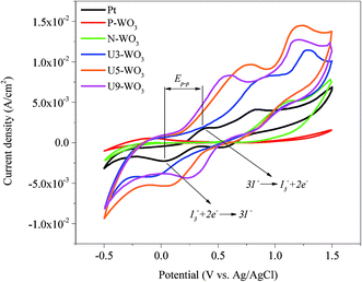
Electrochemical impedance spectroscopy (EIS) is another efficient method to investigate the catalytic performance of counter electrodes. Fig. 9a shows the circuit model used to fit Nyquist plots. Fig. 9b shows the Nyquist plots for pristine WO3 (P-WO3), N2-annealed WO3 (N-WO3), and urea pre-treated WO3 CEs with various urea wt% (U3-WO3, U5-WO3, and U9-WO3). The fitted results were calculated and are listed in Table 2. Two arcs were seen in Nyquist plots. The left arc in the high-frequency range is assigned to the charge transfer resistance (RCT) and capacitance (CPE) at the electrolyte/CE interface while the second arc on the right is assigned to the Nernst diffusion impedance (ZN) of redox ions in the electrolyte. The high-frequency intercept at the x-axis represents the internal series resistance (RS) of CE. The fitted results showed that the pristine P-WO3 CE electrode has poor catalytic activity towards the redox electrolyte due to its high RCT and RS values. The catalytic performance of WO3 CE was increased by annealing in the N2 atmosphere due to the introduction of OVs which act as active sites for triiodide ion reduction. The catalytic activity was further improved by applying urea pre-treatment as shown in the U3-WO3 and U5-WO3 CEs. The improvement in catalytic performance is due to the increase of reduction active sites (OVs) by increasing urea wt% with optimum catalytic performance for U5-WO3 CE, which showed the lowest RCT and RS values. By increasing urea wt% to 9 wt%, the catalytic performance of U9-WO3 was slightly decreased. This could be due to excess OVs introduced which can cause charge accumulation at the interface between the electrolyte and U9-WO3 CE.72 With regard to capacitance, Pt CE showed the lowest capacitance values compared to all WO3-based CEs. This could be attributed to the planar surface of Pt. It is noticed that Pt CE has the lowest ZN value compared to all WO3-based CEs. This could be due to the combination of both Nernst diffusion impedance and the porous diffusion impedance in the porous WO3-based CEs.73
 |
| | Fig. 9 (a) Equivalent circuit model used to fit Nyquist plots for dummy cells of counter electrodes. (b) Nyquist plots of pristine WO3 (P-WO3), N2-annealed (N-WO3) WO3, urea pre-treated WO3 CEs with different urea wt% (U3-WO3, U5-WO3, and U9-WO3) and Pt CE. | |
Table 2 Calculated Tafel and EIS fitted parameters extracted from Nyquist plots of respective dummy cells from pristine WO3 (P-WO3), N2-annealed (N-WO3) WO3, urea pre-treated WO3 CEs with different urea wt% (U3-WO3, U5-WO3, and U9-WO3) in comparison to the Pt CE cell
| Counter electrode |
R
s (Ω cm2) |
R
ct (Ω cm2) |
C (F cm−2) |
Z
N (Ω) |
Exchange current density (Jo) (mA cm−2) |
Limiting current density (Jlim) (mA cm−2) |
| Pt |
2.33 |
2.2 |
5.1 × 10⁻⁶ |
2.56 |
1.1 |
17.68 |
| P-WO3 |
3.57 |
83 |
8.14 × 10⁻⁵ |
— |
0.0026 |
0.676 |
| N-WO3 |
2.66 |
2.93 |
1 × 10⁻⁴ |
10.24 |
0.0175 |
3.28 |
| U3-WO3 |
2.58 |
0.83 |
4 × 10⁻⁴ |
7.1 |
0.256 |
10.37 |
| U5-WO3 |
2.19 |
0.65 |
1.76 × 10⁻³ |
3.7 |
1.923 |
16.69 |
| U9-WO3 |
2.23 |
0.72 |
1.82 × 10⁻³ |
4.47 |
1.488 |
14.44 |
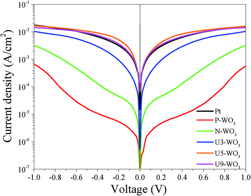
Fig. 10 shows Tafel polarization curves measured for the dummy cells of counter electrodes. Tafel curves could be recognized by three potential zones: polarization zone (|V| < 120 mV), Tafel zone with the mid-range of potential (with a sharp slope), and the diffusion zone at high potential (horizontal part).70,74–76 In the Tafel zone, a larger slope for the anodic and cathodic branches indicates a higher exchange current density (Jo) which is inversely proportional to the charge transfer resistance (RCT) according to eqn (8).70,76
| |  | (8) |
where
R is the gas constant,
T is the absolute temperature, and
F is Faraday's constant.
Table 2 shows that
Jo values are inversely proportional to the measured
RCT values with the highest
Jo value for U5-WO
3 CE which also has the lowest value of
RCT. In addition, the limiting current density (
Jlim), which is the value of current density at high voltage ∼(−1, 1 V), is related to the diffusion coefficient of redox ions as expressed in
eqn (9).
70,76| | 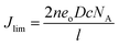 | (9) |
where
NA is the Avogadro constant,
l is the spacer thickness,
D is the diffusion coefficient, and other parameters have been defined previously.
77Table 2 shows that Pt CE has higher
Jlim than the other WO
3-based CEs due to its lower Nernst diffusion impedance
ZN as calculated from EIS fitting. U5-WO
3 CE has the second highest value of
Jlim while P-WO
3 CE has the lowest
Jlim. The results are consistent with EIS fitted parameters.
 |
| | Fig. 10 Tafel polarization curves of symmetrical dummy cells of pristine WO3 (P-WO3), N2-annealed WO3 (N-WO3), pre-treated N2-annealed WO3 with 3 wt% (U3-WO3), 5 wt% (U5-WO3), and 9 wt% (U9-WO3) urea, and Pt CE. | |
Fig. 11 shows J–V curves for DSSC devices with pristine WO3 (P-WO3), N2-annealed WO3 (N-WO3), urea pre-treated WO3 CEs with different urea wt% (U3-WO3, U5-WO3, and U9-WO3). The short circuit current (JSC), open circuit voltage (VOC), and fill factor (FF) are summarized in Table 3. The pristine (P-WO3) CE-based device showed the lowest photovoltaic performance with PCE of ∼3.3%. The PCE increased to ∼8.4% by just annealing in N2 for N-WO3 CE. The improvement in PCE is attributed to the OVs introduced after annealing in the N2 atmosphere. The urea pre-treatment further increased the PCE to 9.7% and 10.5% for U3-WO3 and U5-WO3, respectively. All photovoltaic parameters including JSC, VOC and FF were improved after urea pretreatment. The highest device performance including a JSC of ∼20 mA cm−2, VOC of ∼0.86 V, FF of ∼61% and PCE of 10.5% were achieved for the U5-WO3 CE. However, increasing the urea wt% to 9 wt% for U9-WO3 CE reduces the overall device PCE to ∼9.67%. This could be caused by the charge recombination probability at the interface between the electrolyte and U9-WO3 CE.72 Compared to Pt, the U5-WO3 CE-based device showed higher PCE of 10.5% versus ∼9.3% for the Pt-based device.
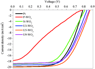 |
| | Fig. 11
J–V characteristic curves for pristine WO3 (P-WO3), N2-annealed WO3 (N-WO3), pre-treated N2-annealed WO3 with 3 wt% (U3-WO3), 5 wt% (U5-WO3), and 9 wt% (U9-WO3) urea, and Pt CE. | |
Table 3 Photovoltaic parameters of P-WO3, N-WO3, U3-WO3, U5-WO3, U9-WO3 and Pt CE
| Counter electrode |
J
SC (mA cm−2) |
V
OC (volt) |
FF (%) |
PCE (%) |
| Pt |
19.94 ± 0.06 |
0.78 |
60 ± 0.2 |
9.33 ± 0.34 |
| P-WO3 |
17.74 ± 0.08 |
0.78 |
24 ± 1 |
3.32 ± 0.15 |
| N-WO3 |
18.93 ± 0.05 |
0.81 |
55 ± 1 |
8.43 ± 0.18 |
| U3-WO3 |
19.29 ± 0.1 |
0.84 |
60 ± 0.6 |
9.72 ± 0.15 |
| U5-WO3 |
20.03 ± 0.05 |
0.86 |
61 ± 0.7 |
10.5 ± 0.154 |
| U9-WO3 |
18.75 ± 0.03 |
0.86 |
60 ± 0.1 |
9.67 ± 0.04 |
In order to demonstrate the effect of surface voids on the catalytic performance of WO3 CE, the oxygen vacancy effect of the U5-WO3 CE-based device was excluded by annealing the counter electrode in ambient air for 1 hour. The obtained oxidized WO3 electrode (O-WO3) has similar surface morphology to that of U5-WO3 CE without oxygen vacancies. The power conversion efficiency (PCE) of O-WO3 based DSSCs was only ∼4.6% while that of U5-WO3 CE based DSSCs was ∼10.5%. Fig. S2 (ESI†) shows the photovoltaic performance of DSSC devices fabricated with both U5-WO3 and O-WO3. In Fig. S2,† oxygen vacancies in U5-WO3 play a significant role in DSSC performance indicated by the higher fill factor and open circuit voltage. On the other hand, the photovoltaic performance of the O-WO3 based DSSC device is significantly low at ∼4.6%.
4. Conclusions
In summary, we demonstrated urea pre-treatment as a new and facile method to activate commercial WO3 as the CE for substantially improved catalytic performance. Oxygen vacancies were created by urea pretreatment. Oxygen vacancies acted as in-gap states to facilitate electron transfer for efficient tri-iodide ion reduction. This process improved the overall catalytic performance of metal oxide CEs. The number of oxygen vacancies was optimized by optimizing the urea wt% used for the pre-treatment. The U5-WO3 CE-based device achieved a PCE of ∼10.5%, which was an improvement from the reference Pt CE-based device at ∼9.3% and non-active WO3 CE based cell at 3.32%.
Conflicts of interest
There are no conflict to declare.
Acknowledgements
This study was partially supported by the US-Pakistan Joint Science and Technology through National Academy of Science, NSF MRI program and Egyptian government fellowship (Egyptian Missions sector) for Dr Elbohy.
References
- B. O'Regan and M. Gratzel, Nature, 1991, 353, 737–740 CrossRef.
- X. Mei, S. J. Cho, B. Fan and J. Ouyang, Nanotechnology, 2010, 21, 395202 CrossRef PubMed.
- P. Poudel, A. Thapa, H. Elbohy and Q. Qiao, Nano Energy, 2014, 5, 116–121 CrossRef CAS.
- A. Aboagye, H. Elbohy, A. D. Kelkar, Q. Qiao, J. Zai, X. Qian and L. Zhang, Nano Energy, 2015, 11, 550–556 CrossRef CAS.
- Y. Jo, J. Y. Cheon, J. Yu, H. Y. Jeong, C.-H. Han, Y. Jun and S. H. Joo, Chem. Commun., 2012, 48, 8057–8059 RSC.
- A. Kay and M. Grätzel, Sol. Energy Mater. Sol. Cells, 1996, 44, 99–117 CrossRef CAS.
- M. Sekkarapatti Ramasamy, A. Nikolakapoulou, D. Raptis, V. Dracopoulos, G. Paterakis and P. Lianos, Electrochim. Acta, 2015, 173, 276–281 CrossRef CAS.
- P. Joshi, X. Yu, M. Ropp, D. Galipeau, S. Bailey and Q. Qiao, Energy Environ. Sci., 2008, 2, 426–429 Search PubMed.
- G. Sai-Anand, A.-I. Gopalan, K.-P. Lee, S. Venkatesan, B.-H. Kang, S.-W. Lee, J.-S. Lee, Q. Qiao, D.-H. Kwon and S.-W. Kang, Sol. Energy Mater. Sol. Cells, 2015, 141, 275–290 CrossRef CAS.
- M. Li, S. K. Cushing, J. Zhang, J. Lankford, Z. P. Aguilar, D. Ma and N. Wu, Nanotechnology, 2012, 23, 115501 CrossRef PubMed.
- M. Wang, A. M. Anghel, B. t. Marsan, N.-L. Cevey Ha, N. Pootrakulchote, S. M. Zakeeruddin and M. Grätzel, J. Am. Chem. Soc., 2009, 131, 15976–15977 CrossRef CAS PubMed.
- J. Zhao, A. Wang and M. A. Green, Prog. Photovolt: Res. Appl., 1999, 7, 471–474 CrossRef CAS.
- M. Wu, X. Lin, A. Hagfeldt and T. Ma, Angew. Chem., Int. Ed., 2011, 50(15), 3520–3524 CrossRef CAS PubMed.
- M. A. Green, J. Zhao, A. Wang and S. R. Wenham, IEEE Trans. Electron Devices, 1999, 46, 1940–1947 CrossRef CAS.
- J. Zhao, A. Wang, M. A. Green and F. Ferrazza, Appl. Phys. Lett., 1998, 73, 1991–1993 CrossRef CAS.
- B. O'regan and M. Grfitzeli, Nature, 1991, 353, 737–740 CrossRef.
- M. Grätzel, Inorg. Chem., 2005, 44, 6841–6851 CrossRef PubMed.
- C. Longo and M.-A. De Paoli, J. Braz. Chem. Soc., 2003, 14, 898–901 CrossRef.
- M. Wu, X. Lin, W. Guo, Y. Wang, L. Chu, T. Ma and K. Wu, Chem. Commun., 2013, 49, 1058–1060 RSC.
- M. Wu, X. Lin, L. Wang, W. Guo, Y. Wang, J. Xiao, A. Hagfeldt and T. Ma, J. Phys. Chem. C, 2011, 115, 22598–22602 CAS.
-
K. Hara, Dye-sensitized solar cells, in Handbook of Photovoltaic Science and Engineering, ed. S. H. A. Luque, John Wiley & Sons, Ltd, 2003 Search PubMed.
- F. Cheng, T. Zhang, Y. Zhang, J. Du, X. Han and J. Chen, Angew. Chem., Int. Ed., 2013, 52, 2474–2477 CrossRef CAS PubMed.
- G. Wang, Y. Yang, D. Han and Y. Li, Nano Today, 2017, 13, 23–39 CrossRef CAS.
- H. Song, M. Luo and A. Wang, ACS Appl. Mater. Interfaces, 2017, 9, 2875–2882 CAS.
- Z. Wang, Y. You, J. Yuan, Y.-X. Yin, Y.-T. Li, S. Xin and D. Zhang, ACS Appl. Mater. Interfaces, 2016, 8, 6520–6528 CAS.
- H.-S. Kim, J. B. Cook, H. Lin, J. S. Ko, S. H. Tolbert, V. Ozolins and B. Dunn, Nat. Mater., 2017, 16, 454–460 CrossRef CAS PubMed.
- F. Lei, Y. Sun, K. Liu, S. Gao, L. Liang, B. Pan and Y. Xie, J. Am. Chem. Soc., 2014, 136, 6826–6829 CrossRef CAS PubMed.
- M. Rioult, D. Stanescu, E. Fonda, A. Barbier and H. Magnan, J. Phys. Chem. C, 2016, 120, 7482–7490 CAS.
- A. M. Smith, M. G. Kast, B. A. Nail, S. Aloni and S. W. Boettcher, J. Mater. Chem. A, 2014, 2, 6121–6129 CAS.
- M. Wu, Y. Wang, X. Lin, A. Hagfeldt and T. Ma, ChemCatChem, 2012, 4, 1255–1258 CrossRef CAS.
- S.-Q. Fan, B. Fang, J. H. Kim, B. Jeong, C. Kim, J.-S. Yu and J. Ko, Langmuir, 2010, 26, 13644–13649 CrossRef CAS PubMed.
- Z. Huang, X. Liu, K. Li, D. Li, Y. Luo, H. Li, W. Song, L. Chen and Q. Meng, Electrochem. Commun., 2007, 9, 596–598 CrossRef CAS.
- D. Song, Z. Chen, P. Cui, M. Li, X. Zhao, Y. Li and L. Chu, Nanoscale Res. Lett., 2015, 10, 16 CrossRef PubMed.
- M. Koebel and E. O. Strutz, Ind. Eng. Chem. Res., 2003, 42, 2093–2100 CrossRef.
- Z. Lendzion-Bielun, U. Narkiewicz and W. Arabczyk, Materials, 2013, 6, 2400 CrossRef CAS PubMed.
- T. Bell and L. Torrente-Murciano, Top. Catal., 2016, 59, 1438–1457 CrossRef CAS.
- A. K. Hill and L. Torrente-Murciano, Int. J. Hydrogen Energy, 2014, 39, 7646–7654 CrossRef CAS.
- S. Phanichphant, Procedia Eng., 2014, 87, 795–802 CrossRef CAS.
- C. Prajapati and P. Sahay, J. Nano- Electron. Phys., 2011, 3, 714 Search PubMed.
- G. Wang, Y. Ling, H. Wang, X. Yang, C. Wang, J. Z. Zhang and Y. Li, Energy Environ. Sci., 2012, 5, 6180–6187 CAS.
- R. Chandra Sekhar, H. Manu, A. Govindaraj and C. N. R. Rao, Nanotechnology, 2007, 18, 205504 CrossRef.
- S. Shubhda, J. Kiran, V. N. Singh, S. Sukhvir, N. Vijayan, D. Nita, G. Govind and T. D. Senguttuvan, Nanotechnology, 2012, 23, 205501 CrossRef PubMed.
- H. Li, J. Xu, Y. Zhu, X. Chen and Q. Xiang, Talanta, 2010, 82, 458–463 CrossRef CAS PubMed.
- M. Tiemann, Chem.–Eur. J., 2007, 13, 8376–8388 CrossRef CAS PubMed.
- T. Waitz, T. Wagner, T. Sauerwald, C.-D. Kohl and M. Tiemann, Adv. Funct. Mater., 2009, 19, 653–661 CrossRef CAS.
- G. Korotcenkov, Mater. Sci. Eng., B, 2007, 139, 1–23 CrossRef CAS.
- N. Pinna, G. Neri, M. Antonietti and M. Niederberger, Angew. Chem., 2004, 116, 4445–4449 CrossRef.
- C. Wang, L. Yin, L. Zhang, D. Xiang and R. Gao, Sensors, 2010, 10, 2088 CrossRef CAS PubMed.
- H. Meixner, J. Gerblinger, U. Lampe and M. Fleischer, Sens. Actuators, B, 1995, 23, 119–125 CrossRef CAS.
- M. M. Khan, S. F. Adil and A. Al-Mayouf, J. Saudi Chem. Soc., 2015, 19, 462–464 CrossRef.
- X. Fu, L. A. Clark, Q. Yang and M. A. Anderson, Environ. Sci. Technol., 1996, 30, 647–653 CrossRef CAS.
- M. Anpo, H. Nakaya, S. Kodama, Y. Kubokawa, K. Domen and T. Onishi, J. Phys. Chem., 1986, 90, 1633–1636 CrossRef CAS.
- J. Zhang, Y. Wu, M. Xing, S. A. K. Leghari and S. Sajjad, Energy Environ. Sci., 2010, 3, 715–726 CAS.
- Y. Inoue, Energy Environ. Sci., 2009, 2, 364–386 CAS.
- X. Wang, K. Maeda, A. Thomas, K. Takanabe, G. Xin, J. M. Carlsson, K. Domen and M. Antonietti, Nat. Mater., 2009, 8, 76–80 CrossRef CAS PubMed.
- X. Chen, L. Liu and F. Huang, Chem. Soc. Rev., 2015, 44, 1861–1885 RSC.
- X. Chen, L. Liu, P. Yu and S. Mao, Science, 2011, 331, 746–750 CrossRef CAS PubMed.
- A. Naldoni, M. Allieta, S. Santangelo, M. Marelli, F. Fabbri, S. Cappelli, C. L. Bianchi, R. Psaro and V. Dal Santo, J. Am. Chem. Soc., 2012, 134, 7600–7603 CrossRef CAS PubMed.
- A. Sinhamahapatra, J.-P. Jeon, J. Kang, B. Han and J.-S. Yu, Sci. Rep., 2016, 6, 27218 CrossRef CAS PubMed.
- S. A. Ansari, M. M. Khan, S. Kalathil, A. Nisar, J. Lee and M. H. Cho, Nanoscale, 2013, 5, 9238–9246 RSC.
- D. Mohammad Mansoob Khan, M. E. Khan and M. H. Cho, RSC Adv., 2016, 6, 20824–20833 RSC.
- S. J. Hong, S. Lee, J. S. Jang and J. S. Lee, Energy Environ. Sci., 2011, 4, 1781–1787 CAS.
- W. Morales, M. Cason, O. Aina, N. R. de Tacconi and K. Rajeshwar, J. Am. Chem. Soc., 2008, 130, 6318–6319 CrossRef CAS PubMed.
- A. M. Elseman, D. Rayan and M. Rashad, J. Mater. Sci.: Mater. Electron., 2016, 27, 2652–2661 CrossRef CAS.
- M. M. Rashad and A. E. Shalan, Appl. Phys. A: Mater. Sci. Process., 2014, 116, 781–788 CrossRef CAS.
-
S. O. Kapap, Principles of Electronic Materials
and Devices, Tata McGraw Hill Education Private limited, New Delhi, 2007 Search PubMed.
- A. Sinhamahapatra, J.-P. Jeon, J. Kang, B. Han and J.-S. Yu, Sci. Rep., 2016, 6, 27218 CrossRef CAS PubMed.
- H. Elbohy, A. Aboagye, S. Sigdel, Q. Wang, M. H. Sayyad, L. Zhang and Q. Qiao, J. Mater. Chem. A, 2015, 3, 17721–17727 CAS.
- J. D. Roy-Mayhew, D. J. Bozym, C. Punckt and I. A. Aksay, ACS Nano, 2010, 4, 6203–6211 CrossRef CAS PubMed.
- F. Gong, X. Xu, Z. Li, G. Zhou and Z.-S. Wang, Chem. Commun., 2013, 49, 1437–1439 RSC.
- K. Yu, Z. Wen, H. Pu, G. Lu, Z. Bo, H. Kim, Y. Qian, E. Andrew, S. Mao and J. Chen, J. Mater. Chem. A, 2013, 1, 188–193 CAS.
- N. K. Elumalai, A. Saha, C. Vijila, R. Jose, Z. Jie and S. Ramakrishna, Phys. Chem. Chem. Phys., 2013, 15, 6831–6841 RSC.
- D. Song, Z. Chen, P. Cui, M. Li, X. Zhao, Y. Li and L. Chu, Nanoscale Res. Lett., 2015, 10, 16 CrossRef PubMed.
- S. Yun, L. Wang, C. Zhao, Y. Wang and T. Ma, Phys. Chem. Chem. Phys., 2013, 15, 4286–4290 RSC.
- X. Zheng, J. Deng, N. Wang, D. Deng, W. H. Zhang, X. Bao and C. Li, Angew. Chem., Int. Ed., 2014, 53, 7023–7027 CrossRef CAS PubMed.
- F. Gong, H. Wang, X. Xu, G. Zhou and Z.-S. Wang, J. Am. Chem. Soc., 2012, 134, 10953–10958 CrossRef CAS PubMed.
- A. Hauch and A. Georg, Electrochim. Acta, 2001, 46, 3457–3466 CrossRef CAS.
Footnote |
| † Electronic supplementary information (ESI) available. See DOI: 10.1039/c7se00483d |
|
| This journal is © The Royal Society of Chemistry 2018 |

 ab,
Khan Mamun
Reza
a,
Salem
Abdulkarim
a and
Qiquan
Qiao
ab,
Khan Mamun
Reza
a,
Salem
Abdulkarim
a and
Qiquan
Qiao