
Silver bismuth iodides in various compositions as potential Pb-free light absorbers for hybrid solar cells†
Ki Woo
Jung
a,
Mi Rae
Sohn
a,
Hye Min
Lee
a,
In Seok
Yang
a,
Sang Do
Sung
a,
Jeongho
Kim
 *a,
Eric
Wei-Guang Diau
b and
Wan In
Lee
*a
*a,
Eric
Wei-Guang Diau
b and
Wan In
Lee
*a
aDepartment of Chemistry and Chemical Engineering, Inha University, Incheon 22212, Korea. E-mail: wanin@inha.ac.kr; jkim5@inha.ac.kr
bDepartment of Applied Chemistry, Institute of Molecular Science, National Chiao Tung University, Hsinchu 30010, Taiwan
First published on 7th November 2017
Abstract
Polycrystalline silver bismuth iodide (SBI) powders of various compositions (Ag![[thin space (1/6-em)]](https://www.rsc.org/images/entities/char_2009.gif) :Bi = 2:1–1:1 in atomic ratio) were synthesized via a solid-state reaction in an evacuated Pyrex tube. Regardless of the composition of Ag and Bi, Ag2BiI5 in the hexagonal phase was preferentially formed and BiI3 impurity in the rhombohedral phase was formed with the increase of the Bi component. The synthesized SBI powders of various compositions were applied as light absorbers for hybrid solar cells (HSCs), which employ mesoporous TiO2 as the electron transporting layer and pristine spiro-OMeTAD as the hole transporting layer. To deposit light absorber layers, the coating solutions were prepared by dissolving the synthesized SBI powders in DMSO/DMF/HI and spin-coated over the mesoporous TiO2 layer. For the solar cell employing pure Ag2BiI5, a photovoltaic conversion efficiency (PCE) of 1.74% was achieved, whereas the inclusion of the BiI3 impurities in the Ag2BiI5 phase significantly increased the device performance. The highest PCE of 2.31% was achieved with the SBI of Ag:Bi = 55:45. Furthermore, the SBI solar cells show no hysteresis in the J–V curve measurements and are highly stable under ambient conditions, exhibiting excellent long-term stability at a relative humidity of 50%.
:Bi = 2:1–1:1 in atomic ratio) were synthesized via a solid-state reaction in an evacuated Pyrex tube. Regardless of the composition of Ag and Bi, Ag2BiI5 in the hexagonal phase was preferentially formed and BiI3 impurity in the rhombohedral phase was formed with the increase of the Bi component. The synthesized SBI powders of various compositions were applied as light absorbers for hybrid solar cells (HSCs), which employ mesoporous TiO2 as the electron transporting layer and pristine spiro-OMeTAD as the hole transporting layer. To deposit light absorber layers, the coating solutions were prepared by dissolving the synthesized SBI powders in DMSO/DMF/HI and spin-coated over the mesoporous TiO2 layer. For the solar cell employing pure Ag2BiI5, a photovoltaic conversion efficiency (PCE) of 1.74% was achieved, whereas the inclusion of the BiI3 impurities in the Ag2BiI5 phase significantly increased the device performance. The highest PCE of 2.31% was achieved with the SBI of Ag:Bi = 55:45. Furthermore, the SBI solar cells show no hysteresis in the J–V curve measurements and are highly stable under ambient conditions, exhibiting excellent long-term stability at a relative humidity of 50%.
Introduction
All-solid-state hybrid solar cells (HSCs), consisting of a thin light absorber layer, a mesoporous inorganic electron transporting layer (ETL), and an organic hole transporting layer (HTL), have been diversely investigated over the last decade.1–10 In particular, perovskite solar cells (PSCs), which employ methylammonium lead halide (CH3NH3PbX3, X = I, Br or Cl) in the perovskite structure, have attracted great interest as next generation solar cells primarily due to their remarkable photovoltaic conversion efficiency (PCE) over 20%.11–18 Among several methylammonium lead halides, CH3NH3PbI3 is an excellent light absorber with a bandgap (1.55 eV) appropriate for utilization of solar light, a high molar absorption coefficient, extremely low exciton binding energy, an abnormally long charge diffusion length, and others. Moreover, CH3NH3PbI3-based PSCs are much cheaper to fabricate than typical silicon solar cells, because the major components constituting the PSC devices are cheap and core parts of the device can be fabricated by a simple wet-chemical process.16–19 Also, processes for large-area fabrication as well as flexible devices are now under development.20–26 However, for the commercial application of PSC devices, several obstacles still need be overcome. Especially, Pb contained in perovskite light absorbers is a harmful element to our environment and has to be replaced by environmentally benign elements. Also, the poor stability of Pb-containing perovskite materials has to be overcome. Thus, it is important to develop Pb-free light absorbers with extended stability for the commercialization of PSC devices in the near future.As a Pb-free light absorber, Sn-based perovskite materials have often been investigated.27–32 By replacing Pb2+ with Sn2+, CH3NH3SnI3 can be synthesized by a simple solution process under inert conditions. CH3NH3SnI3 has a narrower bandgap (1.23 eV) than CH3NH3PbI3, which is more advantageous for utilizing the solar spectrum.32 Thus far, a PCE over 6% has been achieved,32 but CH3NH3SnI3 has even poorer stability than CH3NH3PbI3 because Sn2+ contained in CH3NH3SnI3 is readily oxidized to Sn4+ under ambient conditions. Recently, Bi- and Sb-based light absorbers such as (CH3NH3)3Bi2I9,33–35 (CH3NH3)3Sb2I9,36 Cs3Sb2I9 (ref. 37) and others were also investigated because Sb and Bi are much less harmful than Pb and the light absorbers containing these elements have excellent molar absorption coefficients of the order of 105 cm−1. However, HSCs employing the light absorbers containing Bi or Sb exhibited photovoltaic conversion efficiencies (PCEs) of only less than 0.5% in most cases, except Zhang et al.'s recent report (PCE = 1.64%).35 The reason for such low PCEs has not been clearly understood yet, but high exciton binding energy of those materials as well as difficulty of morphology control for their films might be responsible for the low PCE.36,37 Double perovskite-type Cs2AgBiX6 (X = Br, Cl) structures were also investigated, but their band gaps turned out to be too large for application in light absorbers and significant photovoltaic performances were not acquired.38–40 Mathews et al. studied the series of (CH3NH3)2CuClxBr4−x, belonging to 2-dimensional copper perovskite, but the achieved PCE from (CH3NH3)2CuCl2Br2 was only 0.017%.41
Recently, silver-bismuth halides have been investigated as a potential light absorber for solar cells.42–47 Sargent et al. prepared AgBi2I7 in the cubic phase with a bandgap of 1.87 eV, and achieved a PCE of 1.22% by applying it as a light absorber of HSCs.45 Johansson et al. prepared Ag2BiI5 in the hexagonal phase with the bandgap of 1.85 eV, and reported a PCE of 2.1%.46 Very recently, Turkevych et al. prepared silver-bismuth iodides of various compositions by a solid-state reaction in an evacuated silica tube at 600 °C.47 Among them, Ag3BiI6 in the R3m rudorffite structure with the bandgap of 1.79–1.83 eV was reported to be the most efficient material for light absorbers. The fabricated FTO/mesoporous TiO2/Ag3BiI6/PTAA/Au solar cell showed a noticeable PCE of 4.3%. The obtained results suggest that silver-bismuth halide materials can be a potential candidate for Pb-free light absorbers of perovskite solar cells. Furthermore, silver-bismuth halides offer significantly better stability than methylamine lead halides because they are not hygroscopic under ambient conditions.
In this work, we synthesized various silver bismuth iodides (SBIs) in the composition range of Ag:Bi = 2:1–1:1 by a solid-state reaction at 500 °C. Regardless of the composition in this range, Ag2BiI5 in the hexagonal phase was preferentially formed, whereas the AgBiI4 phase was not formed at all. Instead, the rhombohedral BiI3 phase was included in addition to the Ag2BiI5 phase. The obtained result suggests that the Ag2BiI5 phase is the most stable one among the SBI phases formed in the composition range of Ag:Bi = 2:1–1:1. We also found that the PSC devices employing the SBI with excess Bi showed significantly higher cell performance compared to those employing pure Ag2BiI5. We optimized the composition of SBI and discussed the role of the BiI3 impurity phase mixed with Ag2BiI5 in enhancing the cell performance.
Results and discussion
Polycrystalline silver bismuth iodide (SBI) powders in the composition range of Ag:Bi = 2:1–1:1 were prepared via a solid-state reaction in an evacuated Pyrex tube. Fig. 1a shows the XRD patterns of SBI powders with the Ag-to-Bi molar ratios of 67:33, 60:40, 55:45, and 50:50. In spite of the compositional variation in this range, the Ag2BiI5 in the hexagonal phase (ICDD cards 00-023-1025) was the main phase for all of the synthesized powders. The pure Ag2BiI5 phase was formed from the AgI and BiI3 powders mixed with a molar ratio of 67:33 (SBI-67:33). When the Ag to Bi ratio was 60:40, the BiI3 peaks were not observed by XRD analysis within the detection limit, but noticeable BiI3 diffraction peaks were detected for the SBI in the composition of 55:45 (SBI-55:45). That is, an additional peak at 26.98° is identified to be the (11![[3 with combining macron]](https://www.rsc.org/images/entities/char_0033_0304.gif) ) peak of the rhombohedral BiI3 phase (ICDD cards 00-007-0269). In the SBI samples prepared with the Ag-to-Bi molar ratio of 50:50 (SBI-50:50), the intensity of the BiI3 peak further increases, but the major component is still the hexagonal Ag2BiI5 phase, and the AgBiI4 phase was not formed.43 The obtained result is compatible with the phase diagrams of silver bismuth iodides reported by Babanly et al.48Fig. 1b shows the photographic and scanning electron microscopy (SEM) images of the as-prepared SBI-67:33 (pure Ag2BiI5) and SBI-55:45 powders. Both samples exhibit a blackish color, and the individual particles have a kind of plate-like structure.
) peak of the rhombohedral BiI3 phase (ICDD cards 00-007-0269). In the SBI samples prepared with the Ag-to-Bi molar ratio of 50:50 (SBI-50:50), the intensity of the BiI3 peak further increases, but the major component is still the hexagonal Ag2BiI5 phase, and the AgBiI4 phase was not formed.43 The obtained result is compatible with the phase diagrams of silver bismuth iodides reported by Babanly et al.48Fig. 1b shows the photographic and scanning electron microscopy (SEM) images of the as-prepared SBI-67:33 (pure Ag2BiI5) and SBI-55:45 powders. Both samples exhibit a blackish color, and the individual particles have a kind of plate-like structure.
 | ||
| Fig. 1 XRD patterns of the polycrystalline SBI powders in various Ag to Bi molar ratios prepared by a solid-state reaction at 500 °C and the BiI3 powder in the rhombohedral phase (a), photographic and SEM images of Ag2BiI5 (SBI-67:33) and SBI-55:45 powders (b), and XRD patterns of the Ag2BiI5 films deposited on the FTO/TiO2 by the coating solutions of Ag2BiI5 powder and the mixture of AgI and BiI3, respectively (c). XRD patterns of the bare FTO/TiO2 substrate are also included. | ||
For the formation of SBI films, the synthesized SBI powders were dissolved in a mixed solvent of DMF/DMSO/HI and the prepared solution was then spin-coated on the mesoporous TiO2 layer, followed by heat treatment at 120 °C. The XRD patterns of the SBI-67:33 film, as shown in Fig. 1c, reveal that the film has the same crystallographic phase as the initial Ag2BiI5 powder. As a control experiment, a film was prepared from a simple mixture of AgI and BiI3 with a molar ratio of 67:33, that is, without the SBI synthesis. The XRD patterns of the control film sample are also shown in Fig. 1c, showing that the diffraction peaks representing the Ag2BiI5 phase are not as intense as those of the film derived from the synthesized SBI powder. This result clearly indicates that the coating solution prepared from the SBI powders is much more effective in forming the highly crystallized phase in the fabricated film.
UV-visible absorption spectra were obtained for the SBI-67:33 (that is, pure Ag2BiI5) and SBI-55:45 films deposited on the mesoporous TiO2 layer, as shown in Fig. 2a. The absorption spectra of these two films of the same thickness are quite similar to each other in the overall shape, but we reproducibly monitored that the SBI-55:45 film shows relatively higher absorbance. Compared with the CH3NH3PbI3 film of the same thickness, these two films exhibit appreciably higher absorbance in the wavelength range of 550–650 nm, suggesting that the prepared SBI materials are well suited for harvesting the solar light. Details for the SBI-67:33, SBI-55:45 and CH3NH3PbI3 films used for the measurement of the absorption spectra are described in Fig. S1.†
 | ||
| Fig. 2 Absorption spectra of Ag2BiI5, SBI-55:45, and CH3NH3PbI3 films coated on the mesoporous TiO2 layer (a), and Tauc plots of Ag2BiI5 and SBI-55:45 films (b). Thickness of each film over the mesoporous TiO2 layer was controlled to ∼60 nm for the comparison of absorbance. | ||
The absorption band edge of the SBI-67:33 and SBI-55:45 films was estimated to be ∼680 nm, and their band gaps were determined to be 1.88 and 1.83 eV, respectively, according to the Tauc plots shown in Fig. 2b. On the other hand, the quantum yield of photoluminescence (PL) is very low for both SBI-67:33 and SBI-55:45 with their PL intensities estimated to be less than 1/105 that of CH3NH3PbI3. As a result, the dynamics of charge injection or recombination for SBI-67:33 and SBI-55:45 cannot be determined by conventional time-resolved PL techniques.
The valence band (VB) level of the as-prepared Ag2BiI5 layer coated on the TiO2 layer was determined by ultraviolet photoelectron spectroscopy (UPS). As shown in Fig. 3a, the cutoff energy (Ecutoff) was 16.85 eV, leading to the Fermi level (EF) of 4.37 eV from the equation, EF = 21.22 eV (He I) − Ecutoff. Consequently, the VB level (EVB) of Ag2BiI5 was determined to be −5.63 eV from the EVB − EF value of 1.26 eV obtained by the linear extrapolation in the low binding energy region of the UPS spectrum, as shown in the inset of Fig. 3a. As a result, the conduction band (CB) level of Ag2BiI5 was estimated to be −3.75 eV from its band gap of 1.88 eV, which was determined from the absorption spectrum (see Fig. 2b). Thus, the locations of the VB and CB of Ag2BiI5 are suitable for hybrid solar cells, employing typical ETL materials such as TiO2 and SnO2 and HTL materials such as spiro-OMeTAD and PTAA.49–51 That is, in our solar cell devices, the electrons generated from the Ag2BiI5 can be efficiently injected into the CB of TiO2, while the holes can move into the HOMO level of spiro-OMeTAD, as described in Fig. 3b. A similar behavior is expected for the SBI-55:45 because its major crystallographic phase is Ag2BiI5.
 | ||
| Fig. 3 UPS spectrum for the high binding-energy region of the Ag2BiI5 film coated on the mesoporous TiO2 layer while its low-binding-energy region is shown in the inset (a), and the energy band diagram for charge separation occurring in the Ag2BiI5 solar cell (b). | ||
First of all, pure Ag2BiI5 was employed for the fabrication of solar cells. Ag2BiI5 solutions of various concentrations were prepared by dissolving stoichiometric amounts of the as-prepared pure Ag2BiI5 powders in DMF/DMSO/HI, and each solution was spin-coated on the mesoporous TiO2 layer. The Ag2BiI5 will be deposited into the internal pores as well as overlay-coated on the mesoporous TiO2 layer.
Fig. 4 illustrates plan-view and cross-sectional-view SEM images of the various Ag2BiI5 films prepared from the coating solutions of different concentrations. It was seen from the plan-view SEM images of Fig. 4a that, when the 0.2 M solution of Ag2BiI5 was employed as the coating solution, approximately 50% of the TiO2 surface was covered with Ag2BiI5 grains and the remaining 50% of the TiO2 surface seems to be exposed without the coverage of Ag2BiI5. When employing 0.3 M solution, about 80% of the TiO2 surface is covered by Ag2BiI5. With 0.4 M solution, most of the TiO2 surface is covered by Ag2BiI5 grains except for a few pinholes observed, whereas 0.5 M solution induces complete coverage of the TiO2 surface with Ag2BiI5. From the cross-sectional-view SEM images in Fig. 4b, it can be seen that the thickness of the Ag2BiI5 layer on the TiO2 surface increases to 30, 60, 100 and 150 nm as the concentration of the coating solution increases to 0.2, 0.3, 0.4 and 0.5 M respectively. Fig. 4c shows the cross-section of the fabricated Ag2BiI5 solar cell device with the configuration of FTO/TiO2/Ag2BiI5/spiro-OMeTAD/Au. The thickness of the Ag2BiI5 layer, prepared from a 0.3 M solution, is ∼60 nm, while the thicknesses of mesoporous TiO2, spiro-OMeTAD and the Au counter electrode (CE) layer are ∼220, 150, and 60 nm, respectively.
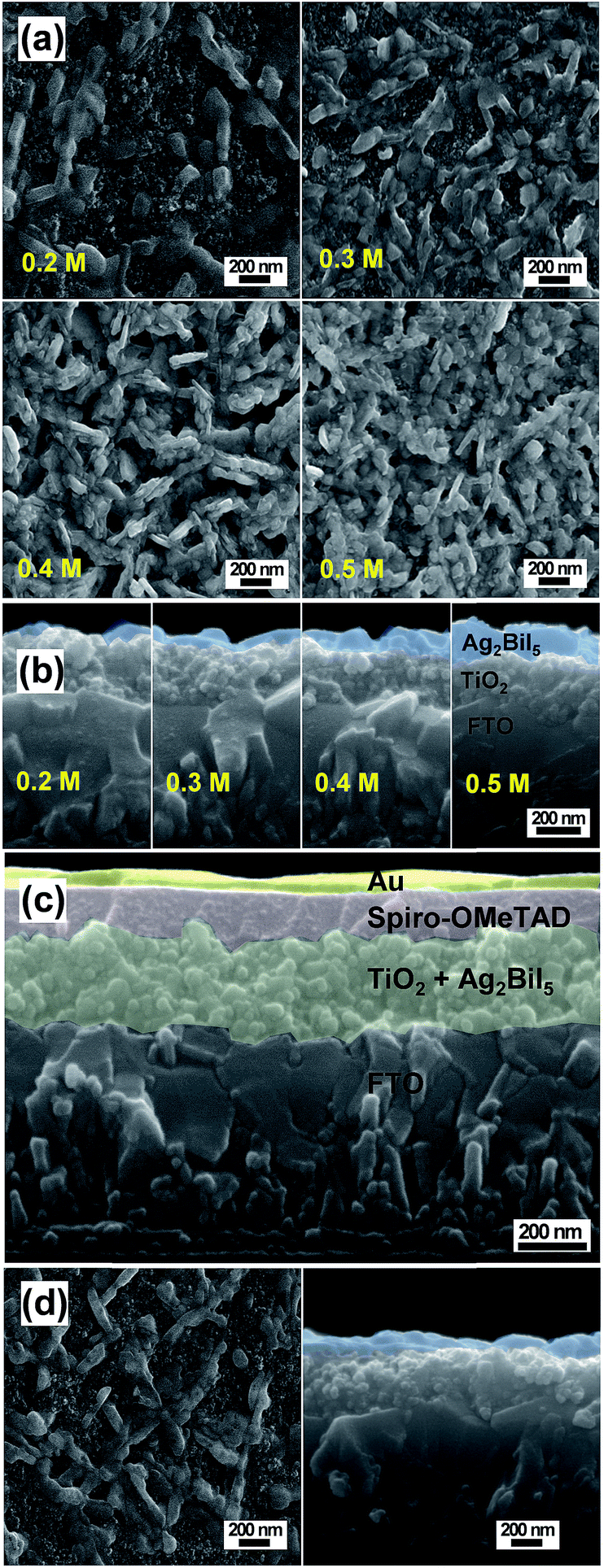 | ||
| Fig. 4 Plan view (a) and cross-sectional view (b) SEM images of Ag2BiI5 layers prepared by the coating solutions of different concentrations, and cross-section of a typical solar cell device employing the Ag2BiI5 layers coated with 0.3 M solution (c). Plan-view and cross-sectional-view SEM images of the SBI 55:45 film coated with 0.3 M solution (d). | ||
J–V curves were measured for the solar cell devices, which have the configuration of FTO/TiO2/Ag2BiI5/spiro-OMeTAD/Au. Fig. 5a shows the J–V curves of the PSC devices employing the Ag2BiI5 layer with various thicknesses. Detailed photovoltaic parameters are listed in Table 1. The solar cell device employing the Ag2BiI5 layer coated with 0.2 M solution gives the PCE of 1.07%, while the device obtained from 0.3 M solution exhibits the PCE of 1.74%, which is the highest value among the Ag2BiI5-based devices. This result is rather unexpected because the mesoporous TiO2 surface is only partially covered with the Ag2BiI5 layer in these devices. In contrast, the Ag2BiI5 films obtained from 0.4 M and 0.5 M solutions show relatively lower PCE values of 1.42 and 1.15%, respectively, although the surface of the TiO2 layer is fully covered by Ag2BiI5 grains.
 | ||
| Fig. 5
J–V curves of the Ag2BiI5 solar cells employing various Ag2BiI5 layers derived from the coating solutions of different concentrations (a) and the solar cell devices employing the various SBI films in different Ag to Bi ratios. (b). IPCE spectra and integrated current densities for the optimized SC-Ag2BiI5 and SC-SBI-55:45 devices (c), and J–V curves of the SC-SBI-55:45 measured under various light intensities (1, 0.7, 0.5, 0.3 and 0.1 sun) (d). | ||
:33 films. Second, the SBI films in various compositions were coated by using the 0.3 M solution. Third, the photovoltaic parameters of SC-SBI-55:45 were obtained under different light intensities. Fourth, PV parameters were obtained by reverse and forward voltage scans
| Solar cells | V OC (mV) | J SC (mA cm−2) | FF (%) | PCE (%) | |
|---|---|---|---|---|---|
| SBIs (Ag:Bi) |
Preparation or measurement conditions | ||||
| 67:33 |
0.2 M | 515 | 4.075 | 51.13 | 1.07 |
| 0.3 M | 592 | 4.898 | 59.96 | 1.74 | |
| 0.4 M | 543 | 4.518 | 57.94 | 1.42 | |
| 0.5 M | 529 | 4.159 | 52.38 | 1.15 | |
| 67:33 |
0.3 M | 592 | 4.898 | 59.96 | 1.74 |
| 60:40 |
596 | 5.640 | 60.73 | 2.04 | |
| 55:45 |
614 | 6.329 | 59.34 | 2.31 | |
| 50:50 |
587 | 5.593 | 58.25 | 1.91 | |
| 55:45 |
1 sun | 612 | 6.116 | 59.21 | 2.22 |
| 0.7 sun | 590 | 4.917 | 57.97 | 2.40 | |
| 0.5 sun | 594 | 4.206 | 54.84 | 2.74 | |
| 0.3 sun | 576 | 2.413 | 51.33 | 2.38 | |
| 0.1 sun | 569 | 0.710 | 54.72 | 2.21 | |
| 55:45 |
Backward | 614 | 6.329 | 59.34 | 2.31 |
| Forward | 618 | 6.235 | 59.20 | 2.28 | |
| 67:33 |
Backward | 592 | 4.898 | 59.96 | 1.74 |
| Forward | 593 | 4.876 | 59.82 | 1.73 | |
To achieve high device performance in hybrid solar cells, in principle, the light absorber layer has to cover the surface of the ETL uniformly and its thickness has to be optimized. That is, full coverage of the TiO2 surface will be advantageous in reducing charge recombination between the electrons in the CB of TiO2 and the holes in the HOMO of the HTM, because TiO2 and the HTM are not in contact with each other in this case. Moreover, the light absorber layer needs to be thick enough to utilize the solar light effectively. In this work, however, the PCE values of the devices with the TiO2 layer fully covered by Ag2BiI5 were significantly lower than those of the devices with the partially covered one. We believe that this observation is closely related to fast recombination between the separated electrons and holes in Ag2BiI5. If the Ag2BiI5 layer is thick, the electrons and holes generated in Ag2BiI5 have to travel long distances to arrive at TiO2 and spiro-OMeTAD, respectively. Hence, charge recombination between electron–hole pairs can occur easily if the charge diffusion coefficients of Ag2BiI5 are small. In our experimental result, optimized photovoltaic performance was achieved with the Ag2BiI5 layer that partially covers the TiO2 surface with a thickness of ∼60 nm, clearly indicating that intrinsically Ag2BiI5 has fast charge recombination properties. According to the energy band diagram shown in Fig. 3b, however, the VOC of the Ag2BiI5-based solar cell is expected to be higher than 1 V, but the obtained VOC value is only 592 mV. This also suggests that significant charge recombination occurs in these solar cell devices.
SBI samples of SBI-60:40, SBI-55:45 and SBI-50:50 were also applied as light absorbers for HSCs. For the coating of each SBI layer, 0.3 M solution was used and the solar cell devices of FTO/TiO2/SBI/spiro-OMeTAD/Au were fabricated by employing the same process that was applied to the Ag2BiI5-based solar cell (SC-Ag2BiI5). Fig. 5b shows the J–V curves of the solar cell devices employing various SBI films. Notably, it was observed that the excess Bi component induces the enhancement of PCE. As a result, the device with SBI-55:45 (SC-SBI-55:45) exhibits the highest efficiency. However, the SBI-50:50 containing higher Bi component leads to relatively lower efficiency. SC-SBI-55:45 showed the optimum PCE of 2.31% with a VOC of 614 mV, JSC of 6.329 mA cm−2, and FF of 59.34%. JSC and VOC values were significantly increased, whereas FF was not appreciably changed, compared to those of SC-Ag2BiI5. Presently, the role of the BiI3 impurity phase in enhancing the cell efficiency is not clear, but higher light absorption of SBI-55:45 than that of SBI-67:33 is one of the major reasons for the increased JSC. In addition, the inclusion of the BiI3 impurity phase seems to be helpful for the electron and hole transport through the Ag2BiI5 layer to TiO2 and Spiro-OMeTAD, respectively, which may cause retardation of charge recombination, thus increasing the VOC.
IPCE spectra were obtained for the SC-Ag2BiI5 and SC-SBI-55:45, as shown in Fig. 5c. The JSC values acquired from the integration of the IPCE spectra match the values acquired from the J–V curves in Fig. 5b. The external quantum efficiency (EQE) maxima for the solar cells with Ag2BiI5 and SBI-55:45 were 35% and 38% at the wavelength of 550 nm. Comparatively low EQE is ascribed to considerable charge recombination occurring in the device.
As shown in Fig. 5d, the J–V curves of the SC-SBI-55:45 were measured at the light intensities in the range of 0.1–1 sun. The maximum PCE of 2.74% was acquired under a light intensity of 0.5 sun. Detailed photovoltaic parameters are listed in Table 1. The obtained result suggests that the SBI-55:45 layer is too thin to completely utilize the photons irradiated from 1 sun. Hence, the amount of SBI-55:45 deposited on the TiO2 layer has to be increased for the complete utilization of solar light. The same trend was also obtained for the SC-Ag2BiI5 devices, as shown in Fig. S2.†
As a control experiment, a 0.3 M SBI-55:45 coating solution was prepared by dissolving stoichiometric amounts of AgI and BiI3 in the mixed solvent of DMF/DMSO/HI. To form the SBI-55:45 layer, the prepared solution was then spin-coated and heat-treated under the same conditions. Fig. S3† shows the J–V curves of the solar cell devices employing two different SBI-55:45 films, derived from the synthesized SBI-55:45 and the mixture of AgI and BiI3, respectively. Herein, the device derived from the mixture of AgI and BiI3 solution showed much poorer efficiency (PCE = 1.10%) with significantly lower JSC and VOC values. The obtained result clearly indicates that the employment of the SBI powders synthesized via a solid-state reaction induces superior photovoltaic performance, presumably due to considerably higher crystallinity in the fabricated SBI films (see Fig. 1c).
SBI-based solar cells are highly stable under ambient conditions, revealing excellent stability at a relative humidity of 50% at 25 °C. Fig. 6a shows the change of PCE as a function of aging time for the SC-SBI-55:45 and SC-SBI-67:33. Extended stability against aging under moisture is ascribed to the intrinsic properties of SBI materials without hygroscopicity. Furthermore, SC-SBI-55:45 as well as SC-SBI-67:33 show negligible hysteresis in the J–V curve measurements, as shown in Fig. 6b and Table 1. The PCE values for backward and forward scans were coincident within measurement error.
 | ||
| Fig. 6 PCE changes of SC-SBI-55:45 and SC-SBI-67:33 as a function of aging time at a relative humidity of 50% at 25 °C (a), and their J–V curves acquired by forward and backward scans at a scan rate of 100 mV s−1 (b). | ||
Regarding the stability and hysteresis, SBI-based solar cells have remarkable advantages. Although SBI-based solar cells in this work show a low cell performance, we expect that the PCE can be improved greatly in the near future, considering that their molar extinction coefficients are comparable to or even higher than CH3NH3PbI3. For the enhancement of PCE in SC-SBI devices, first of all, charge extraction from the SBI layers has to be improved, because Ag2BiI5 and SBI-55:45 show a high rate of charge recombination. In this regard, appropriate materials for the ETL and HTL have to be developed, and the architectures of the ETL or HTL have to be designed for efficient charge collection. In addition, new coating techniques, which facilitate the control of the thickness and grain structure of the SBI layer as well as induce excellent step-coverage over the mesoporous ETL, have to be developed. The interface control at ETL/SBI and SBI/HTL will also be an important issue.
In addition, SBIs with bandgaps of 1.8–1.9 eV are considered to be an appropriate material for the construction of tandem solar cells with high efficiency. At present, GaInP is mainly employed in fabricating the top cell of tandem devices. For instance, the champion PCEs of 31.6% and 32.8% were reported from the tandem devices of GaInP/GaAs and GaInP/Si, respectively.52–54 Considering that the band gaps of SBIs are very close to that of GaInP, SBI solar cells can be a potential candidate for the top cell of tandem devices in the future.
Experimental
Preparation of polycrystalline silver bismuth iodide (SBI) powders
0.1 mol BiI3 (99%, Aldrich) and a stoichiometric amount of AgI (99.9%, Alfa) were mixed and ground for 30 min under an Ar environment. The mixed powder was then inserted into a Pyrex tube and evacuated for 2 h with a mechanical pump. The tube kept at 1.5 ± 0.5 mTorr was sealed using a torch, and subsequently annealed at 500 °C for 12 h. The collected silver bismuth iodide (SBI) powders with a blackish color were gently ground under an Ar environment.Preparation of SBI coating solutions
First, the coating solutions for the SBI film were prepared by dissolving 0.3 g of the as-synthesized SBI powders in the solvent mixture of dimethyl sulfoxide (DMSO), dimethlyformamide (DMF) and HI (57% aqueous solution, Aldrich) with a volume ratio of 3:1:0.2. Particularly, solutions of 0.2, 0.3, 0.4, and 0.5 M concentrations were prepared by varying the amount of mixed solvent added. To obtain neat solutions, the solutions were magnetically stirred for 2 h.
Second, the coating solutions were prepared from the AgI and BiI3 powders. That is, stoichiometric amounts of AgI and BiI3 powders were dissolved in the mixed solvent of DMSO, DMF and HI (3:1:0.2 in volume). Typically, to obtain 0.3 M coating solution for Ag2BiI5 film, 0.141 g AgI, 0.157 g BiI3, and 1.0 mL of the mixed solvent were mixed and stirred for 2 h.
Fabrication of SBI HSCs
The patterned FTO glass (Pilkington, TEC8) was dipped into 1 mM HCl solution for 5 min and washed with deionized water. As a TiO2 compact layer, an ∼10 nm thick Ti film was deposited using a RF magnetron sputtering system (A-Tech system, Korea), followed by oxidation at 500 °C for 30 min in air. A mesoporous TiO2 layer with ∼220 nm thickness was then spin-coated at 7000 rpm for 60 s using the TiO2 paste, which was obtained by diluting the commercial TiO2 paste (DyeSol 18NRT) by 1:6 in volume with the mixed solvent of terpineol and ethanol (2:3 in volume). The coated films were then heated at 500 °C for 30 min. The prepared TiO2 layer was then dipped into 0.2 M TiCl4 solution at 70 °C for 30 min, followed by annealing at 500 °C for 30 min.
Approximately 0.05 mL SBI coating solutions of various concentrations were then dropped onto the mesoporous TiO2 layers. After a stay of 5 s, the films were spun at 4000 rpm for 20 s. To improve the uniformity of the film, 0.5 mL ether was dropped during the spinning. The coated films were then heated on a hot plate at 120 °C for 10 min. Pristine spiro-OMeTAD (2,2′,7,7′-tetrakis(N,N-bis(p-methoxyphenyl)amino)-9,9′-spirobifluorene) was used for the preparation of the HTL because the added additives can react with silver bismuth iodides, as illustrated in Fig. S4.† That is, the solution of 72.3 mg spiro-OMeTAD dissolved in 1.0 mL chlorobenzene without adding any additives was spin-coated at 4000 rpm for 30 s. For the back contact, the Au layer with a thickness of ∼50 nm was deposited by using a thermal evaporator (Korea Vacuum Tech.).
Measurements and characterization
Photocurrent density–voltage (J–V) measurements were performed using a source measurement unit (Model 2400, Keithley). A solar simulator (Model K730, McScience) with AM 1.5G intensity was used as the light source and the light intensity was adjusted using an NREL-calibrated Si solar cell equipped with a KG-5 filter. The solar cell devices were masked with a non-reflective black metal aperture to define the active area, typically 0.122 cm2, while the active area of each device was measured using an optical microscope. In the measurement of J–V curves, the scan rate was 100 mV s−1, and the dwell time before the voltage scan was 20 s. Incident photon-to-current efficiency (IPCE) was measured as a function of wavelength from 300 nm to 800 nm using an IPCE system specially designed for dye-sensitized solar cells (PV Measurements, Inc.).Conclusions
By a solid-state reaction of AgI and BiI3 mixtures in the composition range of Ag:Bi = 2:1–1:1 at 500 °C, polycrystalline Ag2BiI5 powders in the hexagonal phase were preferentially formed with inclusion of the rhombohedral BiI3 impurity phase. It was found that the presence of BiI3 impurities in the Ag2BiI5 phase significantly increased the performance of SBI solar cells. The highest PCE of 2.31% was achieved from the SBI in the composition of Ag:Bi = 55:45, whereas the pure Ag2BiI5 induces only 1.74%. The higher light absorption of SBI-55:45 is considered to be a main reason for the increased JSC. Moreover, the presence of the BiI3 impurity phase may play a favorable role for charge separation in the Ag2BiI5 layer, leading to suppression of charge recombination. In addition, SBI layers derived from the SBI powders synthesized by a solid-state reaction exhibit better performance than those from the mixture of AgI and BiI3 when they were applied as a light absorber layer of the solar cell devices. Furthermore, the fabricated devices reveal no hysteresis in the J–V curve measurements, and are highly stable under ambient conditions, exhibiting excellent long-term stability at a relative humidity of 50% at 25 °C.
Conflicts of interest
There are no conflicts to declare.Acknowledgements
This work has been supported by the Ministry of Science, ICT and Future Planning (MSIP) through the National Research Foundation of Korea (NRF) (2015M1A2A2052999).Notes and references
- H. J. Snaith, S. M. Zakeeruddin, L. Schmidt-Mende Lukas, C. Klein and M. Grätzel, Angew. Chem., Int. Ed., 2005, 44, 6413–6417 CrossRef CAS PubMed.
- H. J. Snaith, A. J. Moule, C. Klein, K. Meerholz, R. H. Friend and M. Grätzel, Nano Lett., 2007, 7, 3372–3376 CrossRef CAS PubMed.
- A. Chang, S. H. Im, Y. H. Lee, H.-J. Kim, C.-S. Lim, J. H. Heo and S. I. Seok, Nano Lett., 2012, 12, 1863–1867 CrossRef PubMed.
- H.-S. Kim, C.-R. Lee, J.-H. Im, K.-B. Lee, T. Moehl, A. Marchioro, S.-J. Moon, R. Humphry-Baker, J.-H. Yum, J. E. Moser, M. Grätzel and N.-G. Park, Sci. Rep., 2012, 2, 591 CrossRef PubMed.
- M. M. Lee, J. Teuscher, T. Miyasaka, T. N. Murakami and H. J. Snaith, Science, 2012, 338, 643–647 CrossRef CAS PubMed.
- J. H. Noh, S. H. Im, J. H. Heo, T. N. Mandal and S. I. Seok, Nano Lett., 2013, 13, 1764–1769 CrossRef CAS PubMed.
- J. Han, Z. Liu, K. Guo, J. Ya, Y. Zhao, X. Zhang, T. Hong and J. Liu, ACS Appl. Mater. Interfaces, 2014, 6, 17119–17125 CAS.
- X. Liu, J. Chen, M. Luo, M. Leng, Z. Xia, Y. Zhou, S. Qin, D.-J. Xue, L. Lv, H. Huang, D. Niu and J. Tang, ACS Appl. Mater. Interfaces, 2014, 6, 10687–10695 CAS.
- Y. Zhou, L. Wang, S. Chen, S. Qin, X. Liu, J. Chen, D.-J. Xue, M. Luo, Y. Cao, Y. Cheng, E. H. Sargent and J. Tang, Nat. Photonics, 2015, 9, 409–415 CrossRef CAS.
- N. G. Park, Mater. Today, 2015, 18, 65–72 CrossRef CAS.
- National Renewable Energy Laboratory, Solar Cell Efficiency Chart, http://www.nrel.gov/ncpv/images/efficiency_chart.jpg, accessed July 2016.
- D. Bi, C. Yi, J. Luo, J. D. Décoppet, F. Zhang, S. M. Zakeeruddin, X. Li, A. Hagfeldt and M. Grätzel, Nat. Energy, 2016, 1, 16142 CrossRef CAS.
- E. H. Anaraki, A. Kermanpur, L. Steier, K. Domanski, T. Matsui, W. Tress, M. Saliba, A. Abate, M. Grätzel, A. Hagfeldt and J. P. Correa-Baena, Energy Environ. Sci., 2016, 9, 3128–3134 CAS.
- W. S. Yang, B.-W. Park, E. H. Jung, N. J. Jeon, Y. C. Kim, D. U. Lee, S. S. Shin, J. Seo, E. K. Kim, J. H. Noh and S. I. Seok, Science, 2017, 356, 1376–1379 CrossRef CAS PubMed.
- H.-S. Kim, J.-Y. Seo and N.-G. Park, ChemSusChem, 2016, 9, 2528–2540 CrossRef CAS PubMed.
- Z. Song, C. L. McElvany, A. B. Phillips, I. Celik, P. W. Krantz, S. C. Watthage, G. K. Liyanage, D. Apul and M. J. Heben, Energy Environ. Sci., 2017, 10, 1297–1305 CAS.
- M. A. Green, A. Ho-Baillie and H. J. Snaith, Nat. Photonics, 2014, 8, 506–514 CrossRef CAS.
- L. K. Ono, N.-G. Park, K. Zhu, W. Huang and Y. Qi, ACS Energy Lett., 2017, 2, 1749–1751 CrossRef CAS.
- X. Liu, F. Kong, R. Ghadari, S. Jin, T. Yu, W. Chen, G. Liu, Z. Tan, J. Chen and S. Dai, Chem. Commun., 2017, 53, 9558–9561 RSC.
- I. Jeong, H. Jung, M. Park, J. S. Park, H. J. Son, J. Joo, J. Lee and M. J. Ko, Nano Energy, 2016, 28, 380–389 CrossRef CAS.
- J. Yoon, H. Sung, G. Lee, W. Cho, N. Ahn, H. S. Jung and M. Choi, Energy Environ. Sci., 2017, 10, 337–345 CAS.
- W. Chen, Y. Wu, Y. Yue, J. Liu, W. Zhang, X. Yang, H. Chen, E. Bi, I. Ashraful, M. Grätzel and L. Han, Science, 2015, 350, 944–948 CrossRef CAS PubMed.
- K.-C. Wang, P.-S. Shen, M.-H. Li, S. Chen, M.-W. Lin, P. Chen and T.-F. Guo, ACS Appl. Mater. Interfaces, 2014, 6, 11851–11858 CAS.
- B. J. Kim, D. H. Kim, Y.-Y. Lee, H.-W. Shin, G. S. Han, J. S. Hong, K. Mahmood, T. K. Ahn, Y.-C. Joo, K. S. Hong, N.-G. Park, S. Lee and H. S. Jung, Energy Environ. Sci., 2015, 8, 916–921 CAS.
- X. Xu, Q. Chen, Z. Hong, H. Zhou, Z. Liu, W.-H. Chang, P. Sun, H. Chen, N. D. Marco, M. Wang and Y. Yang, Nano Lett., 2015, 15, 6514–6520 CrossRef CAS PubMed.
- M. Park, H. J. Kim, I. Jeong, J. Lee, H. Lee, H. J. Son, D.-E. Kim and M. J. Ko, Adv. Energy Mater., 2015, 5, 1501406 CrossRef.
- M. Konstantakou and T. Stergiopoulos, J. Mater. Chem. A, 2017, 5, 11518–11549 CAS.
- M. H. Kumar, S. Dharani, W. L. Leong, P. P. Boix, R. R. Prabhakar, T. Baikie, C. Shi, H. Ding, R. Ramesh, M. Asta, M. Grätzel, S. G. Mhaisalkar and N. Mathews, Adv. Mater., 2014, 26, 7122–7127 CrossRef CAS PubMed.
- T. M. Koh, T. Krishnamoorthy, N. Yantara, C. Shi, W. L. Leong, P. P. Boix, A. C. Grimsdale, S. G. Mhaisalkar and N. Mathews, J. Mater. Chem. A, 2015, 3, 14996–15000 CAS.
- F. Hao, C. C. Stoumpos, D. H. Cao, R. P. Chang and M. G. Kanatzidis, Nat. Photonics, 2014, 8, 489–494 CrossRef CAS.
- Y. He and G. Galli, Chem. Mater., 2014, 26, 5394–5400 CrossRef CAS.
- N. K. Noel, S. D. Stranks, A. Abate, C. Wehrenfennig, S. Guarnera, A.-A. Haghighirad, A. Sadhanala, G. E. Eperon, S. K. Pathak, M. B. Johnston, A. Petrozza, L. M. Herza and H. J. Snaith, Energy Environ. Sci., 2014, 7, 3061–3068 CAS.
- B. W. Park, B. Philippe, X. Zhang, H. Rensmo, G. Boschloo and E. M. J. Johansson, Adv. Mater., 2015, 27, 6806–6813 CrossRef CAS PubMed.
- T. Singh, A. Kulkarni, M. Ikegami and T. Miyasaka, ACS Appl. Mater. Interfaces, 2016, 8, 14542–14547 CAS.
- Z. Zhang, X. Li, X. Xia, Z. Wang, Z. Huang, B. Lei and Y. Gao, J. Phys. Chem. Lett., 2017, 8, 4300–4307 CrossRef CAS PubMed.
- J.-C. Hebig, I. Kühn, J. Flohre and T. Kirchartz, ACS Energy Lett., 2016, 1, 309–314 CrossRef CAS.
- B. Saparov, F. Hong, J.-P. Sun, H.-S. Duan, W. Meng, S. Cameron, I. G. Hill, Y. Yan and D. B. Mitzi, Chem. Mater., 2015, 27, 5622–5632 CrossRef CAS.
- E. T. McClure, M. R. Ball, W. Windl and P. M. Woodward, Chem. Mater., 2016, 28, 1348–1354 CrossRef CAS.
- M. R. Filip, S. Hillman, A. A. Haghighirad, H. J. Snaith and F. Giustino, J. Phys. Chem. Lett., 2016, 7, 2579–2585 CrossRef CAS PubMed.
- R. E. Brandt, V. Stevanovic, D. S. Ginley and T. Buonassisi, MRS Commun., 2015, 5, 265–275 CrossRef CAS.
- D. Cortecchia, H. A. Dewi, J. Yin, A. Bruno, S. Chen, T. Baikie, P. P. Boix, M. Grätzel, S. Mhaisalkar, C. Soci and N. Mathews, Inorg. Chem., 2016, 55, 1044–1052 CrossRef CAS PubMed.
- H. C. Sansom, G. F. Whitehead, M. S. Dyer, M. Zanella, T. D. Manning, M. J. Pitcher, T. J. Whittles, V. R. Dhanak, J. Alaria, J. B. Claridge and M. J. Rosseinsky, Chem. Mater., 2017, 29, 1538–1549 CrossRef CAS.
- Z. Xiao, W. Meng, D. B. Mitzi and Y. Yan, J. Phys. Chem. Lett., 2016, 7, 3903–3907 CrossRef CAS PubMed.
- A. H. Slavney, T. Hu, A. M. Lindenberg and H. I. Karunadasa, J. Am. Chem. Soc., 2016, 138, 2138–2141 CrossRef CAS PubMed.
- Y. Kim, Z. Yang, A. Jain, O. Voznyy, G. H. Kim, M. Liu, L. N. Quan, F. P. García de Arquer, R. Comin, J. Z. Fan and E. H. Sargent, Angew. Chem., Int. Ed., 2016, 55, 9586–9590 CrossRef CAS PubMed.
- H. Zhu, M. Pan, M. B. Johansson and E. M. J. Johansson, ChemSusChem, 2017, 10, 2592–2596 CrossRef CAS PubMed.
- I. Turkevych, S. Kazaoui, E. Ito, T. Urano, K. Yamada, H. Tomiyasu, H. Yamagishi, M. Kondo and S. Aramaki, ChemSusChem, 2017, 10, 3754–3759 CrossRef CAS PubMed.
- L. F. Mashadieva, Z. S. Aliev, A. V. Shevelkov and M. B. Babanly, J. Alloys Compd., 2013, 551, 512–520 CrossRef CAS.
- N. Ahn, D.-Y. Son, I.-H. Jang, S. M. Kang, M. Choi and N.-G. Park, J. Am. Chem. Soc., 2015, 137, 8696–8699 CrossRef CAS PubMed.
- N. J. Jeon, J. H. Noh, Y. C. Kim, W. S. Yang, S. Ryu and S. I. Seok, Nat. Mater., 2014, 13, 897–903 CrossRef CAS PubMed.
- C. Bi, Q. Wang, Y. Shao, Y. Yuan, Z. Xiao and J. Huang, Nat. Commun., 2015, 6, 7747 CrossRef CAS PubMed.
- S. Essig, C. Allebé, T. Remo, J. F. Geisz, M. A. Steiner, K. Horowitz, L. Barraud, J. S. Ward, M. Schnabel, A. Descoeudres, D. L. Young, M. Woodhouse, M. Despeisse, C. Ballif and A. Tamboli, Nat. Energy, 2017, 2, 17144 CrossRef.
- B. M. Kayes, L. Zhang, R. Twist, I.-K. Ding and G. S. Higashi, IEEE J. Photovoltaics, 2014, 4, 729–733 CrossRef.
- J. J. Berry, J. van de Lagemaat, M. M. Al-Jassim, S. Kurtz, Y. Yan and K. Zhu, ACS Energy Lett., 2017, 2, 2540–2544 CrossRef CAS.
Footnote |
| † Electronic supplementary information (ESI) available: Supplementary SEM images and J–V curves of solar cell devices are included. See DOI: 10.1039/c7se00477j |
| This journal is © The Royal Society of Chemistry 2018 |