
Cryogenically probing the surface trap states of single nanowires passivated with self-assembled molecular monolayers†
Xingyan
Zhao
,
Peng
Tu
,
Jiajing
He
,
Hong
Zhu
and
Yaping
Dan
 *
*
University of Michigan – Shanghai Jiao Tong Uniersity Joint Institute, Shanghai Jiao Tong University, Shanghai 200240, China. E-mail: yaping.dan@sjtu.edu.cn
First published on 21st November 2017
Abstract
Optoelectronically probing the trap state density of single nanoscale devices is a powerful in situ nondestructive technique that is of significance for developing high gain photoconductors by surface engineering. However, the previously demonstrated optoelectronic methods are based on the exponential transient photoresponse assumption and only trap states in a very narrow bandgap region can be probed. In this Letter, we demonstrate a cryogenic technique that is capable of measuring the density of surface trap states in the full half bandgap without the exponential transient photoresponse assumption. The technique is applied to an array of silicon nanowire photoconductors that are fabricated on silicon-on-insulator (SOI) wafer by the top-down approach. Diethyl 1-propylphosphonate (DPP) and hexadecane molecular monolayers are self-assembled on silicon nanowire surfaces as the passivation layer in comparison with dry oxide passivation. The surface trap state density of the dry oxide passivated nanowires exponentially increases from the bandgap center, reaching a peak of ∼5 × 1013 cm−2 eV−1 at 50 meV below the conduction band. The defect state density is significantly suppressed after DPP and hexadecane molecules are grafted onto the nanowire surfaces via covalent bonds. The experimental observations are consistent with the density functional theory calculations.
Highly sensitive nanowire photodetectors may find applications, for instance, as artificial photosensitive neurons due to their small size and flexibility.1–3 Commonly used nanoscale pin photodiodes have no gain and therefore are less sensitive due to weak light absorption. Avalanche photodiodes have high gain but are achieved at high bias voltage,4,5 which is incompatible for low power applications. Nanowire photoconductors, in particular those synthesized by the vapor–liquid–solid method (VLS), are often reported to have extraordinarily high gain thanks to surface trap states.6 However, the VLS synthesized nanowires are extremely challenging for large-scale integration.7 What's more, the VLS method does not have industrial standards. The synthesized nanowires are subject to various size uncertainties and contamination during the growth and processing procedure,7,8 resulting in poorly controlled optoelectronic performances.9,10 Here we employ the standard CMOS process to fabricate an array of silicon nanowire (SiNW) photoconductors with controllable surface quality by patterning silicon-on-insulator (SOI) wafers. Besides the traditional dry oxide passivation, molecular monolayer passivation using hexadecane and diethyl 1-propylphosphonate (DPP) molecules was applied here to form a high quality passivation layer on the silicon nanowire surfaces. By forming covalent bonds on the silicon surfaces, the molecular monolayers can effectively prevent the silicon surfaces from being oxidized and are quite stable to acids, bases and hot solvents.11–14 Although molecular monolayers have been used for device surface passivation, the surface trap state density has yet to be systematically characterized.
The back-gate sweep method has been used to estimate the trap states in thin film devices.15 However, the method would be inaccurate when applied to the nanowires on the Si/SiO2 substrate since the energy band bending at nanowire cylindrical surfaces is uneven. The traditional capacitance–voltage method usually uses a gate-all-around structure to create an even band bending at the nanowire surfaces of different radial directions.16 But the capacitive method often suffers from high noises at the single nanowire level due to ubiquitous parasitic capacitances.16,17 Recently, we developed a non-destructive optoelectronic method that is capable of measuring surface trap states in situ at the single nanowire level.18 The method is unfortunately only applicable to semiconductors that have simple exponential transient photoresponse. And it can only probe the trap states in a very narrow region. If the trap state density near the bandgap edge needs to be measured, a higher light intensity is required. In this case, the small injection condition may not be sustained any more. In the present work, we lower the temperature instead of ramping up the light illumination intensity to shift the minority quasi Fermi level away from Ei, during which EF also shifts away from Ei. As a result, the small injection condition can be readily maintained. This technique will shift the quasi Fermi level in a wide range under the small injection condition, allowing for retrieving the density of trap states to the bandgap edge. We applied this technique to the fabricated nanowire array. The measurements on single nanowire photoconductors clearly show that molecular monolayer passivation using DPP and hexadecane has a higher passivation efficiency than the traditional dry SiO2 passivation.
Si nanowires were fabricated using the top-down method on a SOI substrate with a 200 nm thick device layer on 380 nm thick SiO2. An average boron doping concentration of ∼1 × 1018 cm−3 was achieved by ion implantation. The samples were then annealed at 1000 °C for 30 s after ion implantation to electrically activate the dopants. The nanowires with 8 electrodes were patterned by electron beam lithography and metal evaporation followed by reactive ion etching (RIE). The 6 electrodes between the anode and cathode were designed for four probe and Hall effect measurements. The total length of the nanowires (between the cathode and anode) is 24 μm and the width of the nanowires varies from 200 nm to 1.2 μm. After RIE, the silicon nanowire sample was cleaned in 98% H2SO4![[thin space (1/6-em)]](https://www.rsc.org/images/entities/char_2009.gif) :30% H2O2 (3:1) solution at 85 °C for 15 min, followed by a dip in BOE (6:1) for 30 s. About a 20 nm thick SiO2 passivation layer was grown by furnace annealing at 900 °C for 15 min with an O2 flux of 1000 mL min−1. Photolithography and thermal evaporation of Ti/Au (20 nm/200 nm) films were then performed to form ohmic contacts to the nanowires. The oxide in the metal contact region was removed with HF before metal evaporation. Fig. 1a shows the scanning electron microscopy (SEM) image of a single nanowire device and an array of such devices is shown in the optical microscopy image in Fig. 1b.
:30% H2O2 (3:1) solution at 85 °C for 15 min, followed by a dip in BOE (6:1) for 30 s. About a 20 nm thick SiO2 passivation layer was grown by furnace annealing at 900 °C for 15 min with an O2 flux of 1000 mL min−1. Photolithography and thermal evaporation of Ti/Au (20 nm/200 nm) films were then performed to form ohmic contacts to the nanowires. The oxide in the metal contact region was removed with HF before metal evaporation. Fig. 1a shows the scanning electron microscopy (SEM) image of a single nanowire device and an array of such devices is shown in the optical microscopy image in Fig. 1b.
 | ||
| Fig. 1 (a) SEM false color image of the fabricated SiNW device. The yellow region is metal. (b) Optical microscopic image of the fabricated SiNW array. | ||
The Si NW devices were placed in an optical cryostat (ARS DE-202PI) during the temperature dependent dark current and photocurrent measurements. The back silicon of the SOI wafer is grounded during the measurements. Therefore the back gate effect on the nanowire can be neglected. A sourcemeter (Keithley 2400) was employed to source the dc bias and measure the current. The Si NW device was under the illumination of a diode-pumped solid-state laser (CNI laser MLL-FN-405-400 mW) with a wavelength of 405 nm in the photocurrent measurements. The laser light intensity (6.6 W cm−2) illuminated on the nanowire device was calibrated by using a commercial photodiode (Hamamatsu S5973-02). For the transient photocurrent measurements, the light was cut ON/OFF by using an optical shutter (Thorlabs SH05). For the frequency dependent photocurrent measurements, the light was modulated by using a mechanical chopper and the periodic ac photocurrent was picked up by using a lock-in amplifier (Stanford Research SR830).
Fig. 2a shows the measured dark current Id–V curves of a single Si NW device at different temperatures. The linear Id–V curves indicate that ohmic contacts are formed between the nanowire and metal electrodes. The contact resistance is negligibly small compared to the nanowire resistance, confirmed by four probe measurements. The nanowire resistance increases by 3 orders of magnitude as the temperature lowers from 290 K to 10 K due to the incomplete ionization of boron dopants. Hall effect measurements were conducted and the Hall resistance as a function of magnetic field intensity at different temperatures is shown in Fig. 2b, from which the hole concentration can be found. From the conductivity and hole concentration, we extract the temperature dependent hole mobility, as plotted in the inset of Fig. 2b.
 | ||
| Fig. 2 (a) Measured Id–V curves of a single Si NW device at different temperatures. (b) Hall resistance as a function of magnetic field intensity at varying temperature. Inset: The Hole mobility of the SiNW as a function of temperature. | ||
The frequency dependent ac photoconductance at different temperatures is illustrated in Fig. 3a. The photoconductance all rapidly declines as the chopping frequency increases, due to the fact that the slow capture-emission process of the trap states becomes increasingly difficult to follow the light modulation at higher chopping frequency.18 The photoconductance saturates to a frequency-independent baseline when the chopping frequency is greater than 1 kHz. The saturation photoconductance (σph) is attributed to the combined recombination processes including the Shockley–Read–Hall (SRH) recombination, surface recombination and possible Auger recombination. Optical and electronic simulations were performed using the commercial software Lumerical FDTD and DEVICE (see ESI Fig. S1†). The effective minority carrier lifetime (τeff) can be found by tuning the surface recombination velocity (S) to ensure that the simulated photoconductance is equal to the measured σph. Note that τeff is correlated with S as  in which τb is the lifetime in bulk by the SRH process, and W and H are the width and height of the nanowires (200 nm), respectively. As shown in the inset of Fig. 3a, the lifetime is on the order of nanoseconds and increases at lower temperature, which corresponds to S ∼ 5000 cm s−1. For bulk silicon with a doping concentration of ∼1018 cm−3, the minority carrier lifetime is on the order of microseconds or submicroseconds.19 The observed nanosecond lifetime is dominated by surface recombination, which is often the case for nanoscale devices.20,21 The surface recombination velocity normally decreases as the temperature goes lower,22 resulting in a negative correlation between the minority lifetime and temperature, which is consistent with our observations in Fig. 3a.
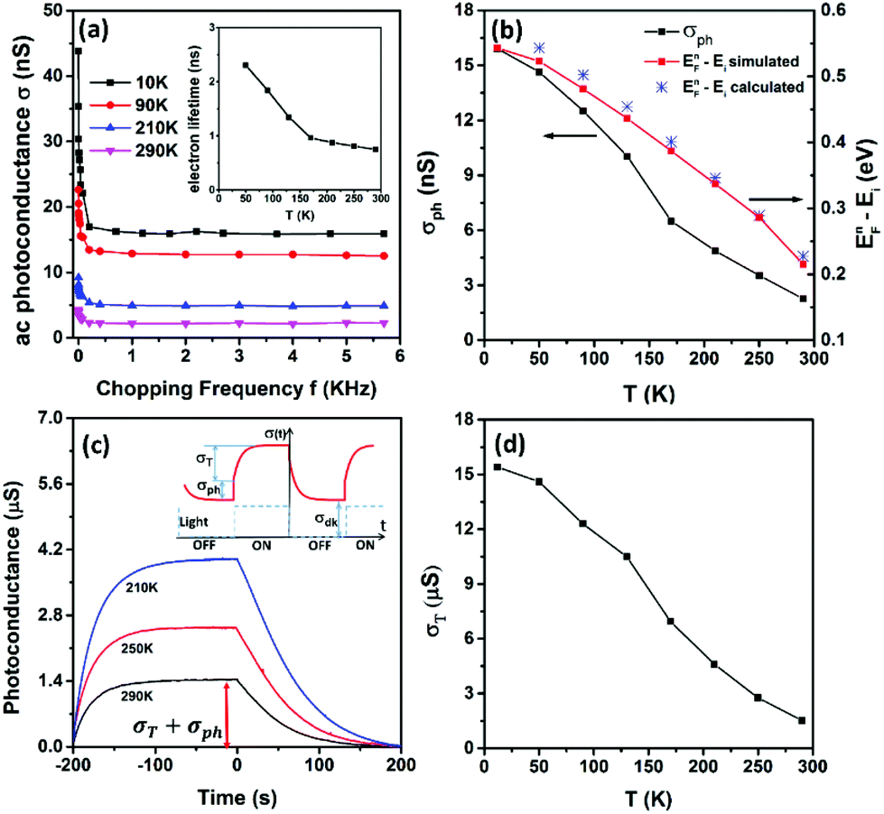 | ||
| Fig. 3 (a) Frequency dependent photoconductance at varying temperature. Inset: The calculated minority electron lifetime. (b) σph and quasi-Fermi energy of electrons as a function of temperature. (c) Measured transient photoconductance of the single Si NW device at different temperatures. Inset: Schematic of the transient response. (d) Trap states induced photoconductance σT as a function of temperature. | ||
As is known, the measured σph is governed by the following equation:
| σph = e(μnΔn + μpΔp)Ac/L | (1) |
 | (2) |
Fig. 3b plots the calculated EFn − Ei as a function of temperature (blue stars). The quasi Fermi level can also be found from the optical and electronic simulations with Lumerical FDTD and DEVICE (red squares, refer to ESI Fig. S1† for simulation details). The calculated and simulated results are consistent with each other. As the temperature is lowered to 10 K from room temperature, EFn shifts from 0.2 eV above Ei to the conduction band edge. What needs to be emphasized here is that the upshift of the minority quasi Fermi level is mainly caused by the decrease of the intrinsic carrier concentration (ni) at lower temperature (see eqn (2) above), instead of larger Δn by stronger light illumination, a strategy that was previously adopted to shift EFn.18,24 As a result, the small injection can be readily satisfied and the trap state density in a wider range can be probed, compared to the previously demonstrated methods.18,24
The typical transient response is depicted in the inset of Fig. 3c. When the light illumination is turned on, the photoconductance jumps up immediately by σph, followed by a slow rise to σT (the inset of Fig. 3c). σph is attributed to the photogenerated electron–hole pairs in the conduction and valence band. The photogenerated excess minority electrons will lift up the electron quasi-Fermi level. Under the small injection condition, the hole quasi-Fermi level (holes are the majority in our case) remains the same as the original Fermi level in the dark. The lift of the electron quasi-Fermi level will allow trap states below it to be filled with the photogenerated excess electrons. The same number of photogenerated hole counterparts is left in the valance band, resulting in a slow rise in photoconductance to σT following the immediate jump. However, for nanoscale devices, σph is often much smaller than σT, resulting in σph buried in the transient response as shown in Fig. 3c. It is highly unreliable to find σph from the transient response,24 in particular, for weak light illumination. In this work, we employed a lock-in amplifier to extract σph at high modulation frequency, as shown in Fig. 3a. The trap-state induced photoconductance σT is found from the total photoconductance in Fig. 3c after deducting σph found in Fig. 3a. σT as a function of temperature is shown in Fig. 3d. Unlike previously demonstrated methods,18,24 here we do not make any assumption such as a single time-constant exponential rise or fall in trap-state induced transient photoconductance which may not be true in some cases.25,26
From Fig. 3d, the surface concentration of excess holes that contribute to the trap induced photoconductance is calculated using the hole mobility in Fig. 2b. The same number of electrons is captured by the trap states below EFn. The density of surface trap states is calculated by simply differentiating the surface concentration of trapped electrons with respect to the electron quasi-Fermi level (see the ESI† for details). The surface trap state density of the dry SiO2 passivated silicon nanowire device is plotted in Fig. 4a. It has a very similar trend to the SiO2 passivated bulk silicon device ((100) plane)27 but with a relatively higher value probably due to the fact that nanowire surfaces of different crystalline orientations are exposed. Indeed, the trap state density measured here is comparable to those previously reported for silicon nanowires at the same energy level.18,24 We also compared the as-fabricated silicon nanowire device with the dry SiO2 passivated device. As expected, a significant reduction of trap state density was observed on the dry SiO2 passivated device (see ESI Fig. S5†). Density functional theory calculations were also performed (see the ESI† for simulation details) and the stick-and-ball sketch of the Si surface dangling bond is shown in Fig. 4b. The simulated surface state density of the SiO2 passivated Si is consistent with the experimental data in terms of the curve shape and peak position, as shown in Fig. 4c.
 | ||
| Fig. 4 (a) Experimental data of surface trap state density distribution of our nanowire devices. Inset: log scale plot. (b) Stick-and-ball sketch of the Si surface showing the local structure of the dangling bond passivated with SiO2, hexadecane and DPP. (c) Simulated density of states for Si slabs passivated with dry oxide, DPP, and hexadecane respectively from density functional theory simulations. (d) Transient photocurrent response of the nanowire devices with different surface passivations. EFn − Ei ∼ 0.26 eV. | ||
Molecular monolayer passivation was performed on two other silicon nanowire samples (with thermal SiO2) using DPP and hexadecane. Before forming metal contacts to the silicon nanowires, the wafers were first etched in BOE 6:1 solution for 90 s to remove the oxide layer and form a Si–H dangling bond for the subsequent self-assembly of the molecular monolayer. One of the two freshly etched silicon wafers was put in the reaction solution (DPP:mesitylene = 2:4 (v/v)) immediately and heated at 120 °C for 3.5 h. The DPP molecules were anchored onto the silicon surfaces by forming Si–O–P covalent bonds (XPS data in the ESI†). The other wafer was put in another reaction solution (hexadecane:mesitylene = 1:10 (v/v)) and heated at 160 °C for 8 h. The hexadecane molecules were grafted on the silicon surface by forming Si–C covalent bonds (XPS data in the ESI†). The whole process was protected under an argon atmosphere (99.999%). The wafers are then cleaned with acetone and DI water after the reaction. Photolithography and thermal evaporation were then performed to form metal contacts to the silicon nanowire device. The surface trap state density of the silicon nanowire devices passivated with DPP and hexadecane monolayers was measured and is plotted in Fig. 4a. Both devices showed a significant reduction of surface trap state density, compared to the SiO2 passivated device. A similar trend was observed in the density functional simulation (Fig. 4c). Nevertheless, the device passivated with hexadecane has a lower surface state density likely due to the fact that hexadecane molecules have a smaller footprint, resulting in more dangling bonds passivated by the molecules. Molecular monolayer passivation is also reported to dictate the temporal response of photoconductive devices.28 The transient current response of the silicon nanowire photoconductor devices passivated with SiO2, DPP and hexadecane is plotted in Fig. 4d. At a given energy level in the bandgap, the emission rate is constant.29 A larger number of carriers trapped at the energy level will take a longer time to emit. At room temperature (Fig. 4d), the electron quasi Fermi level is located around 0.26 eV above the middle bandgap energy level, i.e. EFn − Ei ≈ 0.26 eV. At this energy level, the DPP passivated device has a much longer trap lifetime (tens of seconds) than the SiO2 passivated one due to its much higher trap state density (Fig. 4a). The hexadecane passivated device has a slightly higher trap state density than the SiO2 passivated device, thus the trap lifetime of the hexadecane passivated silicon nanowire photoconductor device is also slightly longer (both are in subseconds). The transient photocurrent response of the three devices at EFn − Ei ≈ 0.40 eV (∼150 K) was also measured (see ESI Fig. S6†) and the trap lifetimes are consistent with the trap state densities at this energy level. The different transient current responses of the SiO2, DPP and hexadecane passivated devices indicate that the trap lifetime can be selectively modified by molecular monolayer passivation.
Conclusions
In this Letter, we have demonstrated a cryogenic method to extract the density of surface trap states at the single nanowire level. Compared to previous capacitive and optoelectronic methods, the technique demonstrated here is more powerful in that trap states in a wider bandgap range can be found with high accuracy. The surface trap state density of silicon nanowire photoconductor devices passivated with DPP and hexadecane molecular monolayers was measured using this cryogenic method. Both the DPP and hexadecane molecular monolayers showed a higher passivation efficiency than dry oxide passivation, which is consistent with the density functional theory calculations.Conflicts of interest
The authors declare no financial competing interests.Acknowledgements
The work is supported by the National Science Foundation of China (61376001 and 21503135). The device microfabrication was performed at the Center for Advanced Electronic Materials and Devices (AEMD), Shanghai Jiao Tong University. Low temperature Hall measurements were conducted at the Instrumental Analysis Center (IAC), Shanghai Jiao Tong University.References
- H. Sohmyung, L. K. Massoud, A. Abraham, J. Yi, D. Samir, K. Yanjin, B. Sue, L. Yu-Hwa, R. F. William, A. S. Gabriel and C. Gert, J. Neural Eng., 2016, 13(5), 056008 CrossRef PubMed.
- S. Jung, J. Shin, K. Pi, Y. Goo and D.-I. Cho, Sensors, 2016, 16(12), 2035 CrossRef PubMed.
- S. Lim, H. Kim, C. Seok, H. Song, S. Lee, S. Jung, H. Yoo, S. Oh, J. Ahn, K. Koo, D.-I. D. Cho and H. Ko, J. Comput. Theor. Nanosci., 2015, 12(5), 769 CrossRef CAS.
- C. Yang, C. J. Barrelet, F. Capasso and C. M. Lieber, Nano Lett., 2006, 6(12), 2929 CrossRef CAS PubMed.
- O. Hayden, R. Agarwal and C. M. Lieber, Nat. Mater., 2006, 5(5), 352 CrossRef CAS PubMed.
- C. Soci, A. Zhang, B. Xiang, S. A. Dayeh, D. Aplin, J. Park, X. Bao, Y.-H. Lo and D. Wang, Nano Lett., 2007, 7(4), 1003 CrossRef CAS PubMed.
- L. VJ, J. Oh, A. P. Nayak, A. M. Katzenmeyer, K. H. Gilchrist, S. Grego, N. P. Kobayashi, S. Y. Wang, A. A. Talin, N. K. Dhar and M. S. Islam, IEEE J. Sel. Top. Quantum Electron., 2011, 17(4), 1002 CrossRef.
- R. G. Hobbs, N. Petkov and J. D. Holmes, Chem. Mater., 2012, 24(11), 1975 CrossRef CAS.
- K. Bradley, J. Cumings, A. Star, J.-C. P. Gabriel and G. Grüner, Nano Lett., 2003, 3(5), 639 CrossRef CAS.
- R. H. Koch and A. Hartstein, Phys. Rev. Lett., 1985, 54(16), 1848 CrossRef CAS PubMed.
- E. J. Nemanick, P. T. Hurley, B. S. Brunschwig and N. S. Lewis, J. Phys. Chem. B, 2006, 110(30), 14800 CrossRef CAS PubMed.
- E. J. Nemanick, P. T. Hurley, L. J. Webb, D. W. Knapp, D. J. Michalak, B. S. Brunschwig and N. S. Lewis, J. Phys. Chem. B, 2006, 110(30), 14770 CrossRef CAS PubMed.
- M. R. Linford, P. Fenter, P. M. Eisenberger and C. E. Chidsey, J. Am. Chem. Soc., 1995, 117(11), 3145 CrossRef CAS.
- A. B. Sieval, A. L. Demirel, J. W. M. Nissink, M. R. Linford, J. H. van der Maas, W. H. de Jeu, H. Zuilhof and E. J. R. Sudholter, Langmuir, 1998, 14(7), 1759 CrossRef CAS.
- H.-C. Lin, C.-H. Hung, W.-C. Chen, Z.-M. Lin, H.-H. Hsu and T.-Y. Hunag, J. Appl. Phys., 2009, 105(5), 054502 CrossRef.
- E. C. Garnett, Y.-C. Tseng, D. R. Khanal, J. Wu, J. Bokor and P. Yang, Nat. Nanotechnol., 2009, 4(5), 311 CrossRef CAS PubMed.
- A. Mesli, J. C. Muller and P. Siffert, Appl. Phys. A, 1983, 31(3), 147 CrossRef.
- Y. Dan, Appl. Phys. Lett., 2015, 106(5), 053117 CrossRef.
- D. B. M. Klaassen, Solid-State Electron., 1992, 35(7), 961 CrossRef CAS.
- Y. Dan, K. Seo, K. Takei, J. H. Meza, A. Javey and K. B. Crozier, Nano Lett., 2011, 11(6), 2527 CrossRef CAS PubMed.
- J. E. Allen, E. R. Hemesath, D. E. Perea, J. L. Lensch-Falk, Z. Y. Li, F. Yin, M. H. Gass, P. Wang, A. L. Bleloch, R. E. Palmer and L. J. Lauhon, Nat. Nanotechnol., 2008, 3(3), 168 CrossRef CAS PubMed.
- M. Ghannam, R. Mertens and R. De Keersmaecker, Physica B+C, 1985, 129(1), 283 CrossRef.
- F. J. Morin and J. P. Maita, Phys. Rev., 1954, 96(1), 28 CrossRef CAS.
- Q. Xu and Y. Dan, Nanoscale, 2016, 8(35), 15934 RSC.
- M. Singh Kamboj, G. Kaur and R. Thangaraj, Thin Solid Films, 2002, 420–421, 350 CrossRef CAS.
- S. K. Tripathi and A. Kumar, J. Electron. Mater., 1988, 17(1), 45 CrossRef CAS.
- X. Y. Zheng and Z. J. Li, Chin. Physics, 1985, 5(2), 478 Search PubMed.
- G. Konstantatos, L. Levina, A. Fischer and E. H. Sargent, Nano Lett., 2008, 8(5), 1446 CrossRef CAS PubMed.
- E. K. Liu, B. S. Zhu and J. S. Luo, Semiconductor Physics, Publishing House of Electronics Industry, Beijing, 2003, p. 154 (in Chinese) Search PubMed.
Footnote |
| † Electronic supplementary information (ESI) available: Simulation details, computational method, XPS data and so on. See DOI: 10.1039/c7nr06925a |
| This journal is © The Royal Society of Chemistry 2018 |