Self-cleaning by harnessing wrinkles in two-dimensional layered crystals
Jia-Sheng
Sun
 a,
Jin-Wu
Jiang
*a,
Harold S.
Park
b and
Sulin
Zhang
cd
aShanghai Institute of Applied Mathematics and Mechanics, Shanghai Key Laboratory of Mechanics in Energy Engineering, Shanghai University, Shanghai 200072, People's Republic of China. E-mail: jwjiang5918@hotmail.com
bDepartment of Mechanical Engineering, Boston University, Boston, Massachusetts 02215, USA
cDepartment of Engineering Science and Mechanics, The Pennsylvania State University, University Park, Pennsylvania 16802, USA
dDepartment of Biomedical Engineering, The Pennsylvania State University, University Park, Pennsylvania 16802, USA
First published on 21st November 2017
Abstract
Two-dimensional (2D) layered crystals are prone to bending and folding owing to their ultra-low bending stiffness. Folds are traditionally viewed as defects that degrade the material performance. Here, we demonstrate that folds and cohesive forces in 2D layered crystals like graphene and MoS2 can be exploited to collect and clean up interlayer impurities, wherein multiple separated impurities agglomerate into a single, large cluster. We combine classical molecular dynamics simulations and an analytical model to elucidate the competing roles of membrane bending and impurity-membrane cohesive energies in the self-cleaning process. Our findings shed light on the mechanisms by which the forces that are present in 2D layered crystals can positively impact, through the possibility of intrinsic cleaning and defect engineering, the synthesis of van der Waals homo- and heterostructures with improved reliability and functionalities.
1. Introduction
Since the successful isolation of graphene, many other planar atomic materials have been isolated using mechanical exfoliation or growth techniques such as chemical vapor deposition, giving rise to a large library of two-dimensional (2D) crystals.1 These isolated atomic planes can be reassembled into 3D van der Waals (vdW) homo- and heterostructures through layer-by-layer stacking.2,3 By rationally choosing both different 2D crystals as the basic building blocks as well as their stacking sequence, the resulting 3D heterostructures may be engineered to compensate for property shortcomings in the constituent 2D crystals, and thus possess unique and tailorable multifunctional properties that open the door for new potential applications centered around 2D materials. However, the preparation, transfer and stacking processes needed to create 2D layered crystals inevitably introduce defects of various kinds, such as intralayer vacancies and interlayer absorbates.4–6 These defects may significantly modify the intrinsic properties of the constituent 2D crystals by functioning as scattering sites or altering the interlayer coupling.7 Interestingly, recent experiments have shown very high carrier mobilities in graphene-hexagonal boron nitride8 and graphene-transition metal dichalcogenide9 heterostructures. This was attributed to the possible self-cleansing processes of the impurities resulting from the high quality of the interfaces. Because the underlying mechanisms governing and enabling the self-cleansing process are still unclear, it is imperative to understand how these impurities interact with the 2D crystals to develop techniques to control and remove the surface and interface impurities.2D crystals represent the thinnest materials in nature. Owing to their ultra-low bending rigidity compared to the in-plane stiffness,10 2D crystals are prone to bending and folding,11 enabling them to conform to rough surfaces and morph into 3D origami with interesting implications for flexible and stretchable electronics.12 More specifically, we note that as the effects of low bending modulus and van der Waals forces on 2D materials have typically been studied independently,2,13 or in the context of controlling the morphology of 2D materials that lie on a substrate,14,15 we demonstrate here that the interplay between bending and cohesion in 2D atomic membranes can be exploited to rearrange, collect, and even clean up interlayer impurities. Specifically, we employ molecular dynamics simulations and analytical modeling to predict the conditions under which self-agglomeration of metallic clusters as interlayer impurities takes place in bilayer graphene and MoS2. Our studies reveal that the interplay between membrane bending and interlayer van der Waals interactions makes the self-agglomeration process cluster-size and cluster-distance dependent. In doing so, we are able to predict the conditions under which self-cleaning takes place in layered 2D materials, like graphene and MoS2.
2. Structure and simulation details
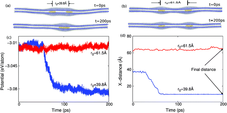
The structure at t = 0 ps in Fig. 1(a) and (b) illustrates two different initial structures of copper clusters sandwiched in between MoS2 layers we simulated using classical molecular dynamics (MD). The copper clusters in Fig. 1(a) and (b) are of spherical shape with a diameter d = 12.7 Å and separated by the initial distance r0. We choose copper to mimic the possibility of metal impurities in MoS2 that might be present from the CVD growth process.16 The objective of the present work is to investigate the conditions that enable these metal impurities to be cleaned by the MoS2 or graphene layers themselves. That is, we will examine the motion of these two copper clusters during the simulation, and determine the conditions under which they merge into one big cluster.The MD simulations were performed within the NPT (i.e. the particle number N, the pressure P and the temperature T of the system are constant) ensemble. The Nosé–Hoover17,18 thermostat was used for maintaining a constant temperature and pressure. Periodic boundary conditions were applied in the two in-plane directions of the 2D material (graphene or MoS2), while free boundary conditions were applied in the out-of-plane direction. The standard Newton equations of motion are integrated in time using the velocity Verlet algorithm with a time step of 1 fs. The MD simulations were performed using the publicly available simulation code LAMMPS.19,20 The OVITO package was used for visualization.21
The embedded-atom method (EAM) potential of Mishin22 was used to describe the interactions among copper atoms, while the MoS2 layers were described by using a recently developed Stillinger–Weber potential.23 The inter-layer van der Waals interaction between two adjacent MoS2 layers was described by using the following 6–12 Lennard-Jones potential,
 | (1) |
We also simulated self-cleaning in bilayer graphene. The interaction between carbon atoms within the same graphene layer is described by using the Brenner potential.26 Parameters for the van der Waals coupling between two graphene layers are ε = 2.96 meV and σ = 3.38 Å.27 The van der Waals interaction between graphene and the copper atom is also described by using the Lennard-Jones potential with parameters ε = 25.78 meV and σ = 3.08 Å.28,29
The simulations were performed in two steps. First, the bilayer structure of either graphene or MoS2 was relaxed to a minimum energy configuration, with the positions of the two copper clusters remaining fixed. The structure at t = 0 ps in Fig. 1(a) and (b) shows the relaxed configuration, in which the two MoS2 layers are combined into a bilayer structure, while the copper clusters are sandwiched by the MoS2 layers. Second, the whole system including the copper clusters was fully relaxed. We will focus on the motion of these two copper clusters in the second step, to determine whether the two copper clusters merge into one bigger cluster, as shown in Fig. 1(a) at t = 200 ps, thus illustrating the self-cleaning phenomenon. It can be seen that the driving force for the self-cleaning phenomenon is the increasing attachment of the top and bottom atomic layers. An example in which the two copper clusters do not self-clean is shown in Fig. 1(b) at t = 200 ps.
During the self-cleaning process, the potential energy of the whole system (including copper and MoS2) decreases suddenly when the self-cleaning phenomenon occurs as shown in Fig. 1(c), where the y-axis is the potential energy per copper atom, i.e., the total energy divided by the number of the copper atoms. The results in Fig. 1(c) are for copper clusters of diameter d = 12.7 Å in bilayer MoS2 of dimensions 210 × 92.8 Å at room temperature. There is a step-like jump in the potential energy curve if the initial distance between these two copper clusters is r0 = 39.8 Å; i.e., the self-cleaning phenomenon occurs. For the initial distance r0 = 61.5 Å, it turns out that the self-cleaning phenomenon does not occur. Accordingly, the potential energy fluctuates around a constant value, and does not show any obvious decrease during the whole simulation process.
Fig. 1(d) shows the change in the centroid distance between two copper metal clusters during the self-cleaning process. The distance decreases suddenly when the self-cleaning phenomenon occurs, i.e. when the initial distance r0 = 39.8 Å. If the initial distance between these two copper clusters is increased to r0 = 61.5 Å, the distance between these two copper clusters does not show any obvious decrease during the whole simulation process, which means that the self-cleaning phenomenon does not occur.
3. Results
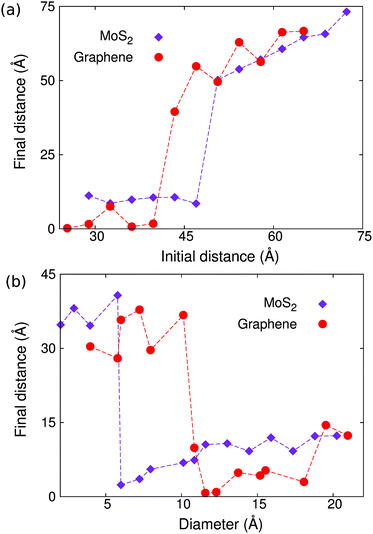
According to Fig. 1, the initial distance between the two copper clusters is crucial for the occurrence of the self-cleaning phenomenon. To quantify the effect of the initial distance, we carried out a set of simulations for a pair of copper clusters with the initial distance r0 increasing from 26 Å to 75 Å, keeping the diameter of the copper cluster d = 11.7 Å unchanged. Fig. 2(a) shows the final distance between the two copper clusters in the structure with different initial distances, which displays a step-like jump at critical values of about r0c = 47.0 Å and r0c = 39.8 Å for MoS2 and graphene, respectively.We also find that the diameter of the copper cluster plays an important role in the self-cleaning phenomenon. We carried out another set of simulations with varying diameters for the copper cluster. The initial distance r0 = 36.2 Å is kept unchanged for this set of simulations. Fig. 2(b) shows the final distance between the two copper clusters versus the diameter of the copper cluster. The critical diameter is about 6.0 Å and 10.8 Å for MoS2 and graphene, respectively, below which the self-cleaning phenomenon will not occur. In Fig. 2(b), because the distance between the clusters is measured as a center to center distance, the final distance is nonzero even through these two copper clusters are combined into a bigger cluster by the self-cleaning process.
From the comparison between the results for MoS2 and graphene in Fig. 2, we find that it is easier for the self-cleaning phenomenon to occur in bilayer MoS2 than in bilayer graphene. That is, the critical value for the initial distance, below which the self-cleaning phenomenon occurs, is larger in MoS2 than graphene. The critical value for the diameter, above which the self-cleaning phenomenon occurs, is smaller in MoS2 than graphene. These results have demonstrated that the self-cleaning phenomenon is dependent on the size of the impurity clusters, the distance separating them, as well as the role of curvature-dependent bending energies along with interlayer van der Waals interactions. In the following section, we will develop a theoretical model to delineate how each of these key factors contributes to the self-cleaning phenomenon.
4. Discussions
A. Peapod mechanism
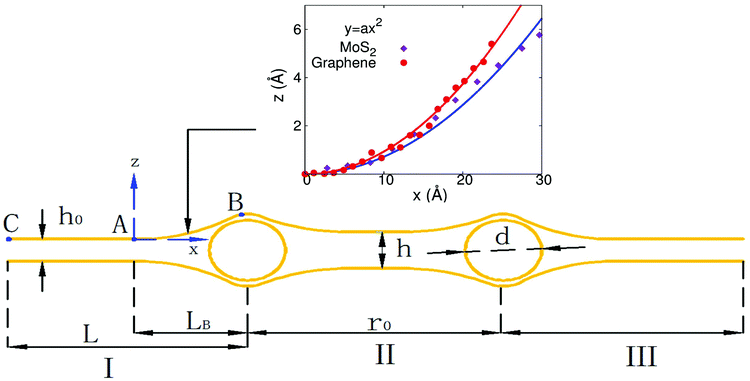
To explore the underlying mechanism of the self-cleaning phenomenon, we noted that the structure simulated in Fig. 1(a) and (b) can be illustrated by using the peapod-like schematic configuration shown in Fig. 3. The atomic layers (MoS2 or graphene) can be divided into three regions by the two copper clusters; i.e., region I (on the left of the left copper cluster), region II (between two copper clusters), and region III (on the right of the right copper cluster). We focus on the left copper cluster. There are two forces generated by the atomic layers in region I on the left copper cluster. The first one is the cohesive or attractive van der Waals force between the atomic layers, which will push the copper cluster to the right. The second one is the bending force induced in segment AB, which also pushes the copper cluster from left to right. The atomic layers in region II also provide cohesive and bending forces on this copper cluster, which tries to push this copper cluster to the left.If the initial distance r0 is large enough, the atomic layers in region II will stick together by the attractive inter-layer van der Waals interaction. In this situation, regions I and II are symmetric about the left copper cluster. As a result, the forces generated by atomic layers from regions I and II will counteract each other, so the net force on the left copper cluster will be too small to induce the self-cleaning phenomenon. However, if the initial distance is small, regions I and II around the left copper cluster become highly asymmetric, which leads to larger separation of the atomic layers in region II. As a result, the cohesive force and bending force provided by atomic layers in region II to resist the self-cleaning phenomenon are quite small, leading to the self-cleaning process.
B. Interplay between cohesion and bending
We next provide an analytical model to derive the critical value for the initial distance separating copper clusters of a specific diameter, and thus provide a more rigorous mathematical description of the physical picture underlying the self-cleaning phenomenon described in the previous section. In Fig. 3, the structure is determined by the diameter (d) of the copper cluster and the initial distance (r0) between two copper clusters. We focus the discussion on the left copper cluster, and first consider the atomic layers in region I. The total length of this segment is L, which is divided into LB and L − LB by point A. The cohesive energy is within the segment AC with length L − LB, while the bending energy is stored in the AB segment that is bent due to the insertion of the copper cluster.The cohesive energy of segment AC is30
 | (2) |
 , W is the width of the atomic layer, s is half of the area of the unit cell, and σ and ε are the Lennard-Jones parameters that describe the van der Waals interactions between layers, where the value of the cohesive parameter γ is −0.0035 eV Å−2 and −0.0184 eV Å−2 for MoS2 and graphene, respectively. We note that there is also cohesive energy between the atomic layers between points A and B. However, this cohesive energy is much smaller than the cohesive energy stored between A and C, because of the larger inter-layer distance induced by the bending, and thus we ignore the cohesive energy in section AB in the following discussion.
To calculate the bending energy in AB, we note that the shape of this segment can be well described by the quadratic function z = ax2, as shown in the inset of Fig. 3. The only parameter a is determined by using the coordinate of B  as
as
 | (3) |
Using the quadratic description for the bending shape, the curvature at position x in segment AB can be obtained as
 | (4) |
The total bending energy is
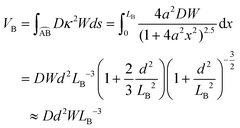 | (5) |
The total energy within region I is the sum of the bending and cohesive energies
| V = VB + VC = Dd2WLB−3 + γW(L − LB). | (6) |
The final stable configuration can be obtained by minimizing the total potential energy with respect to LB, which is achieved at
 | (7) |
 | (8) |
The critical value of the initial distance (r0c) is determined by using the following equation
| r0c = 2LB. | (9) |
Eqn (9) means that the net force on the left copper cluster from its left and right sides is zero if r0 > r0c, because the length of region II is long enough such that the atomic layers are fully adhered together. On the other hand, if r0 < r0c, the atomic layers in region II are not adhered, so the cohesive force and the bending force from region II resisting the motion of the copper cluster are smaller than that from region I. As a result, the net force on the left copper cluster pushes it to the right, leading to the self-cleaning phenomenon.
From eqn (9), we obtain the dependence of the critical initial distance on the diameter of the copper cluster,
 | (10) |
The prefactor on the right hand side of eqn (10) clearly demonstrates the interplay between the impurity cluster size (via d), interlayer cohesive energy (via γ) and curvature energy (via the bending modulus D). It is clear that the critical distance for self-cleaning r0c increases with both increasing curvature energy and impurity cluster size, and decreases with increasing interlayer cohesive energy. Specifically, for a constant cluster diameter d, self-cleaning is possible over larger initial separations or impurity clusters in 2D materials with a larger bending modulus, or weaker cohesive (van der Waals) interactions. In the case of graphene and MoS2, MoS2 has both a significantly larger bending modulus, as well as weaker interlayer cohesive interactions than graphene, which results in a larger critical initial distance for which self-cleaning can occur compared to graphene. We also note that eqn (10) is a universal formula, and can be applicable to other physical processes in 2D membranes where the interplay between bending and cohesion is important, for example during the insertion/extraction of Li in layered anode materials during the cyclic charging/discharging of the Li ion battery.33
This analytical prediction is compared with the MD simulation results in Fig. 4, where we note several features. First, according to eqn (10), the critical distance increases with increasing impurity cluster diameter; so it is easier for the self-cleaning phenomenon to take place if the clusters have a larger diameter, which is indeed observed in the MD simulations. Second, the analytical result predicts that the critical initial distance in MoS2 is much larger than that in graphene. It means that the self-cleaning phenomenon is easier to occur in MoS2 than graphene, which is consistent with the MD simulation results shown in Fig. 2. Fig. 4(a) shows that, for MoS2, the analytical result is in good agreement with the MD simulations. Fig. 4(b) shows that the analytical result is comparable to the MD simulation results for graphene. We note that, for graphene, the critical initial distance predicted by the analytical model is systematically smaller than the MD simulation results, which is likely due to the high flexibility of graphene, which results in a large contact area between graphene and the copper cluster around point B in Fig. 3, and which thus increases the cohesive energy.
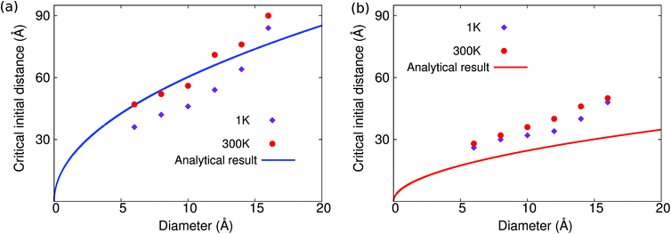 | ||
| Fig. 4 Relationship between the critical initial distance for the self-cleaning phenomenon and the diameter of the copper cluster in (a) MoS2 and (b) graphene. | ||
We see that the critical initial distance predicted by the analytical model is in reasonable agreement with the MD simulation results for MoS2 in Fig. 4(a), whereas the critical initial distance predicted by the analytical model is lower than the MD simulation results in the case of graphene in Fig. 4(b). This underestimation is related to the van der Waals interactions between graphene and the copper cluster, which has been ignored in the analytical model, and which counteracts the driving force (including the cohesive and bending forces) for the self-cleaning phenomenon. Hence, a smaller initial distance is required for the existence of the self-cleaning phenomenon, if the van der Waals interaction between the atomic layer and the copper cluster is considered. As a result, the analytical results will underestimate the critical initial distance in Fig. 4. This agreement is better for MoS2 because the cohesive energy of MoS2 is smaller than that of graphene. Therefore, temperature-induced thermal vibrations have a stronger effect for MoS2 than for graphene, and thus temperature effects are more important than the critical initial distance for MoS2.
It should be noted that the copper clusters that result from the self-cleaning process can be separated from the atomic layered materials. The edge vibration modes localized at the free edges of the layered materials may be able to trap these copper clusters at the free edges, resulting in interesting edge-related phenomena. Finally, we also note that the registry of the two atomic layers may impact the self-cleaning process. For example, AB stacked bilayer graphene has lower energy than AA stacked bilayer graphene, due to the registry dependence of the interlayer coupling. The LJ potential is known to underestimate the registry effect, which may cause some differences if the self-cleaning effect is studied using other stacking sequences.
5. Conclusion
In conclusion, we have demonstrated that folds in 2D crystals can be exploited to rearrange, collect, and clean up interlayer impurities. Our molecular dynamics simulations and theoretical analysis show that the curvature in the form of bending energy drives the agglomeration of interlayer impurities, which is counteracted by the interlayer cohesive energy, resulting in a curve-to-attract phenomenon that has been widely observed in membrane structures. As 2D crystals are prone to folding, with the folds being highly mobile under mechanical stimulation, the agglomerated impurities may be driven toward the edges of the crystals as the folds sweep through the crystalline planes. Our analysis further shows that the self-cleaning process takes place in a manner that depends on the impurity size and the separation distance. Overall, our study sheds new light on the mechanisms by which the forces that are present in 2D layered crystals can positively impact, through the possibility of intrinsic cleaning and defect engineering, the synthesis of vdW homo- and heterostructures with improved reliability and functionalities.Author contributions
J.S.S performed the calculations. J.W.J, H.S.P, and S.Z discussed the results. All authors co-wrote and commented on the paper.Conflicts of interest
The authors declare no competing financial interests.Acknowledgements
The work is supported by the Recruitment Program of Global Youth Experts of China, the National Natural Science Foundation of China (NSFC) under Grant No. 11504225, the start-up funding from Shanghai University, and the Innovation Program of Shanghai Municipal Education Commission under Grant No. 2017-01-07-00-09-E00019. HSP acknowledges the support of the Mechanical Engineering department at Boston University. SZ acknowledges the support by the National Science Foundation (NSF) CMMI-1462980.References
- A. K. Geim and K. S. Novoselov, Nat. Mater., 2007, 6, 183 CrossRef CAS PubMed.
- A. K. Geim and I. V. Grigorieva, Nature, 2013, 499, 419 CrossRef CAS PubMed.
- S. Wang, X. Wang and J. H. Warner, ACS Nano, 2015, 9, 5246 CrossRef CAS PubMed.
- Y. Liu, F. Xu, Z. Zhang, E. S. Penev and B. I. Yakobson, Nano Lett., 2014, 14, 6782 CrossRef CAS PubMed.
- A. Ziletti, A. Carvalho, D. K. Campbell, D. F. Coker and A. C. Neto, Phys. Rev. Lett., 2015, 114, 046801 CrossRef CAS PubMed.
- V. V. Kulish, O. I. Malyi, C. Persson and P. Wu, Phys. Chem. Chem. Phys., 2015, 17, 992 RSC.
- M. Kumar and Y. Ando, J. Nanosci. Nanotechnol., 2010, 10, 3739 CrossRef CAS PubMed.
- S. J. Haigh, A. Gholinia, R. Jalil, S. Romani, L. Britnell, D. C. Elias, K. S. Novoselov, L. A. Ponomarenko, A. K. Geim and R. Gorbachev, Nat. Mater., 2012, 11, 764 CrossRef CAS PubMed.
- A. V. Kretinin, Y. Cao, J. S. Tu, G. L. Yu, R. Jalil, K. S. Novoselov, S. J. Haigh, A. Gholinia, A. Mishchenko and M. Lozada, et al. , Nano Lett., 2014, 14, 3270 CrossRef CAS PubMed.
- X. Meng, M. Li, Z. Kang, X. Zhang and J. Xiao, J. Phys. D: Appl. Phys., 2013, 46, 055308 CrossRef.
- A. Kushima, X. F. Qian, P. Zhao, S. L. Zhang and J. Li, Nano Lett., 2015, 15, 1302 CrossRef CAS PubMed.
- A. M. Stolzenberg and G. S. Haymond, Inorg. Chem., 2002, 41, 300 CrossRef CAS PubMed.
- Q. Lu, M. Arroyo and R. Huang, J. Phys. D: Appl. Phys., 2009, 42, 102002 CrossRef.
- K. Kim, Z. Lee, B. D. Malone, K. T. Chan, B. Alemán, W. Regan, W. Gannett, M. Crommie, M. L. Cohen and A. Zettl, Phys. Rev. B: Condens. Matter Mater. Phys., 2011, 83, 245433 CrossRef.
- N. G. Chopra, L. X. Benedict, V. H. Crespi, M. L. Cohen, S. G. Louie and A. Zettl, Nature, 1995, 377, 135 CrossRef CAS.
- L. Wang, X. Zhang, H. L. Chan, F. Yan and F. Ding, J. Am. Chem. Soc., 2013, 135, 4476 CrossRef CAS PubMed.
- S. Nosé, J. Chem. Phys., 1984, 81, 511 CrossRef.
- W. G. Hoover, Phys. Rev. A, 1985, 31, 1695 CrossRef.
- S. J. Plimpton, J. Comput. Phys., 1995, 117, 1 CrossRef CAS.
- Lammps, http://www.cs.sandia.gov/~sjplimp/lammps.html 2012.
- A. Stukowski, Modell. Simul. Mater. Sci. Eng., 2009, 18(1), 015012 CrossRef.
- Y. Mishin, M. Mehl, D. Papaconstantopoulos, A. Voter and J. Kress, Phys. Rev. B: Condens. Matter Mater. Phys., 2001, 63, 224106 CrossRef.
- J. W. Jiang, Nanotechnology, 2015, 26, 315706 CrossRef PubMed.
- T. Liang, S. R. Phillpot and S. B. Sinnott, Phys. Rev. B: Condens. Matter Mater. Phys., 2009, 79, 245110 CrossRef.
- P. Hirunsit and P. B. Balbuena, J. Phys. Chem. C, 2007, 111, 1709 CAS.
- D. W. Brenner, O. A. Shenderova, J. A. Harrison, S. J. Stuart, B. Ni and S. B. Sinnott, J. Phys.: Condens. Matter, 2002, 14, 783 CrossRef CAS.
- J.-W. Jiang and H. S. Park, J. Appl. Phys., 2015, 117, 124304 CrossRef.
- F. Cleri, S. Yip, D. Wolf and S. R. Phillpot, Phys. Rev. Lett., 1997, 79, 1309 CrossRef CAS.
- D. Wolf and J. Lutsko, J. Mater. Res., 1989, 4, 1427 CrossRef CAS.
- J. H. Zhao, J. W. Jiang, Y. Jia, W. L. Guo and T. Rabczuk, Carbon, 2013, 57, 108 CrossRef CAS.
- J.-W. Jiang, Z. Qi, H. S. Park and T. Rabczuk, Nanotechnology, 2013, 24, 435705 CrossRef PubMed.
- Q. Lu, M. Arroyo and R. Huang, J. Phys. D: Appl. Phys., 2009, 42, 102002 CrossRef.
- E. Yoo, J. Kim, E. Hosono, H.-S. Zhou, T. Kudo and I. Honma, Nano Lett., 2008, 8, 2277 CrossRef CAS PubMed.
| This journal is © The Royal Society of Chemistry 2018 |

