
Construction of 2D-composite HCa2Nb3O10/CaNb2O6 heterostructured photocatalysts with enhanced hydrogen production performance†
Yue
Liu
,
Yansong
Zhou
,
Chade
Lv
,
Congmin
Zhang
,
Xiaoli
Jin
,
Qingqiang
Meng
and
Gang
Chen
 *
*
MIIT Key Laboratory of Critical Materials Technology for New Energy Conversion and Storage, School of Chemistry and Chemical Engineering, Harbin Institute of Technology, 92 West Dazhi Street, Nan Gang District, Harbin, P. R. China. E-mail: gchen@hit.edu.cn
First published on 24th November 2017
Abstract
Semiconductor 2D-composite heterostructures are of great interest in water splitting due to their unique structure. In this work, we design and synthesize 2D-composite HCa2Nb3O10/CaNb2O6 (HCNO/CNO) heterostructured nanosheets for the first time through sintering with a subsequent ion-exchange procedure. The achievement of such a 2D-composite nanostructure is attributed to the similar crystalline structure and intercalation–exfoliation of the layered bulk by employing tetra-n-butylammonium hydroxide (TBA+OH−). Furthermore, the 2D-composite structure contributes to increasing the interfacial contact area and lattice mismatch occurring in the heterostructure. Benefiting from the construction of a heterostructure and the unique structure characteristics, the as-prepared 2D-composite HCNO/CNO nanosheets exhibit rapid photoinduced charge carrier separation and transfer, leading to significantly enhanced photo-electrochemical current response as well as photocatalytic hydrogen evolution.
Introduction
Photocatalytic water-splitting for hydrogen production utilizing semiconducting materials is essential to answer global environmental pollution and the energy crisis as an economical technique.1–7 Among the state-of-the-art photocatalysts, the layered perovskite-type niobates exhibit outstanding photocatalytic properties owing to their anisotropic features, single-crystalline texture and high surface area.8–14 HCa2Nb3O10 obtained by chemically replacing the K+ of layered Dion–Jacobson perovskite KCa2Nb3O10 with H+, possessing high chemical durability and nontoxicity, has been suggested as one of the high-efficiency photocatalysts for hydrogen production.15–18 However, the photochemical water splitting capability of HCa2Nb3O10 is limited by its rapid carrier recombination.19–22 The creation of heterostructures coupled with other semiconductors is considered to be an alternative way of promoting the separation and transfer efficiency of photogenerated carriers.23–27 Nevertheless, inherent limitations such as poor lattice mismatch and interfacial contact exist in the heterostructured photocatalysts caused by the incompatibility between various materials.28,29 Therefore, it is of significance to craft an ingenious heterojunction to address the above-mentioned obstacles.30,31Very recently, many kinds of novel 2D-composite heterostructured photocatalysts have been designed and adequately demonstrated to show excellent lattice mismatch and interfacial contact. Hence, facilitated carrier transfer at heterostructured interfaces is realized, resulting in enhanced catalytic properties.32–35 For instance, He's group presented an in situ synthesis approach to obtain 2D-composite porous nitrogen-doped carbons (PNCs@Gr) showing remarkable cycling stability contributed by their unique structure.36 In addition, Chai and coworkers reported 2D-composite graphene–g-C3N4 nanocomposites by an innovative 2D interface engineering approach, exhibiting a 2.3-fold enhancement over pure g-C3N4 due to the lower recombination rate of charge carriers at the heterostructured interface.37 Sun and his partners synthesized BiOI(001)/BiOCl(010) with a greater degree of lattice mismatch displaying higher visible-light photocatalytic activity than BiOI(001)/BiOCl(001) with a higher ηCI value.38 Inspired by these excellent pioneer achievements, the construction of 2D-composite heterostructures might dramatically improve the photocatalytic performance of HCa2Nb3O10.
Currently, the proposition of rational strategies for constructing HCa2Nb3O10 based 2D-composite heterostructure is in great demand.39 The heterostructure that is formed by consistent element composition contributes to favorable interfacial contact.40 Therefore, it could possibly be most important to explore a semiconductor possessing a similar structure and element composition to HCa2Nb3O10 to prepare a 2D-composite heterostructure with excellent lattice mismatch and interfacial contact. Calcium niobate (CaNb2O6) has a similar perovskite-like structure and element composition to HCa2Nb3O10.41
Consequently, it is envisaged that the introduction of element-copied CaNb2O6 to construct a heterostructure with HCa2Nb3O10 might realize a 2D-composite heterostructured photocatalyst, but up until now it has remained unexplored.
In this study, as shown in Fig. 1, 2D-composite HCa2Nb3O10/CaNb2O6 (HCNO/CNO) heterostructured nanosheets were successfully fabricated through exfoliating and restacking layered HCNO/CNO which were obtained through sintering materials with a subsequent ion-exchange procedure for the first time. The 2D-composite heterostructure endows the photocatalysts with favorable interfacial contact. Moreover, interfacial lattice mismatch appears in the 2D-composite heterostructure profiting from the semblable crystalline structure of HCNO and CNO. Thanks to the above merits, boosted charge carrier transfer is achieved, which is proved by photoelectrochemistry and photoluminescence spectra (PL). Significantly, the 2D-composite HCNO/CNO sample exhibits about 2 times increase in hydrogen production in contrast with pristine HCNO.
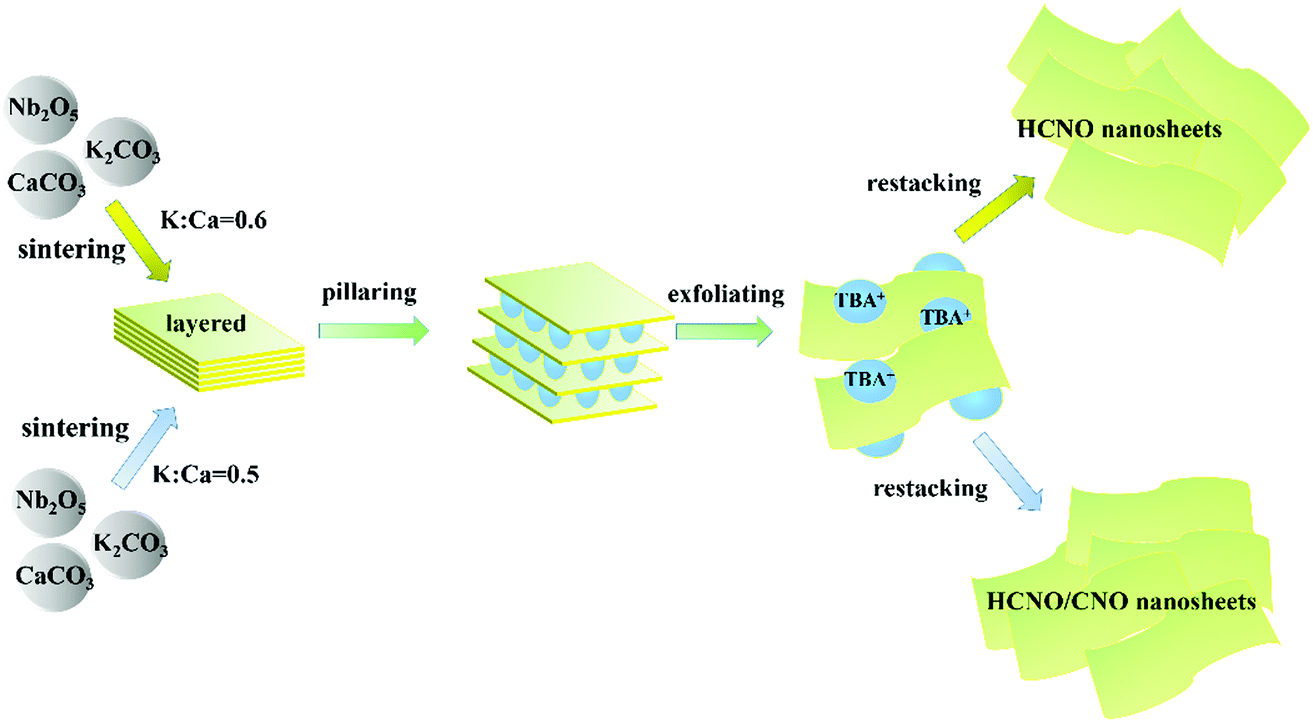 | ||
| Fig. 1 Schematic illustration of the synthesis process of the HCNO and HCNO/CNO nanosheets via sintering with a subsequent ion-exchange procedure. | ||
Results and discussion
The X-ray diffraction (XRD) patterns in Fig. 2 reveal the crystallographic structure and phase purity of the as-prepared samples. Pure CaNb2O6 (CNO) and HCNO were also synthesized as references by just adjusting the molar ratio of potassium and calcium in the raw materials. In the XRD pattern of HCNO/CNO, all the diffraction peaks can be perfectly indexed as HCa2Nb3O10 (JCPDS, No. 39-0915) and CaNb2O6 (JCPDS, No. 39-1392), indicating that well-crystallized HCNO/CNO is successfully synthesized in this work. | ||
| Fig. 2 XRD patterns of the pure CNO, HCNO and HCNO/CNO samples. | ||
The morphologies of the as-prepared HCNO/CNO were investigated by scanning electron microscopy (SEM). As shown in Fig. 3a, the HCNO/CNO nanosheets with smooth surfaces exhibit a sheet-like morphology with a thickness of about 40–60 nm. The top view (planar nanosheets) and side view (perpendicular nanosheets) of the HCNO/CNO nanosheets which simultaneously appear in the TEM image (Fig. 3b) show an alike thickness with the SEM image. Fig. 3c gives the high resolution TEM (HRTEM) of the top view for the HCNO/CNO nanosheets from Section 1 of Fig. 3b. As observed in Fig. 3b, the interplanar distances of 0.38 nm and 0.75 nm are consistent with the d-spacing of the (100)HCNO and (020)CNO planes. Meanwhile, both of the two lattice planes are parallel to each other, being likely to cause the interfacial lattice mismatch. The corresponding selected area electron diffraction (SAED) pattern, which is the same as the simulated pattern, is shown in the inset image of Fig. 3d. It displays the characteristic spots for an orthorhombic structure, suggesting the reflections of the (100) and (110) planes for HCNO, and the (200) and (130) planes for CNO, respectively, implying the co-existence of both HCNO and CNO in the heterostructured nanosheets. Furthermore, it also verifies that the heterostructure is produced by the connection of (001)HCNO and (001)CNO.
 | ||
| Fig. 3 SEM image (a), TEM image (b), and HRTEM image (c) of the HCNO/CNO nanosheets and the corresponding SAED patterns (d) of (b). | ||
In order to analyze the structural characteristics of the 2D-composite heterostructure more distinctly, the structural model of the atomic arrangement and the simulated diagram of the planes were established as shown in Fig. 4. The structural model (left) indicates that interfacial lattice mismatch might occur between the (001) planes of layered perovskite-related type HCNO and CNO. Both the intersection angles of (020)CNO and (010)HCNO, and (200)CNO and (100)HCNO are about 0°. Combining two kinds of crystalline interplanar spacing (Fig. 4 right) finds a couple of (010)HCNO planes that are approximately equal to a (020)CNO plane, and besides, a couple of (100)HCNO planes approach the sum of three (200)CNO planes. All the analysis results demonstrate that interfacial lattice mismatch occurs in the HCNO/CNO heterostructure. During the formation of a semiconductor heterostructure, interfacial lattice mismatch plays an important role which is helpful to the transfer of charge carriers on account of high structural strain.42a–c In our case, the interfacial lattice mismatch between the (020)CNO and (010)HCNO planes is about 2.73%, and that between the (200)CNO and (100)HCNO planes is about 3.04%. The low interfacial lattice mismatch can promote the separation of carriers due to the production of a less defective and abrupt interface.
 | ||
| Fig. 4 Structural model of the atomic arrangement on the different views of HCNO/CNO and schematics of the heterostructure interface between (010)HCNO and (020)CNO or (100)HCNO and (200)CNO, suggesting their low interfacial lattice mismatch. | ||
The UV-Vis diffuse reflectance spectra (DRS) of the samples are displayed in Fig. 5. All the samples exhibit an absorption edge at ca. 370 nm, indicating that the construction of a 2D-composite heterostructure has no impact on the photo absorption ability of HCNO.
 | ||
| Fig. 5 UV-vis spectra for the pure CNO, HCNO and HCNO/CNO samples. | ||
In order to analyze the surface chemical composition and chemical states of the HCNO/CNO nanosheets, X-ray photoelectron spectroscopy (XPS) measurements were carried out (Fig. 6). Nb, O and Ca are found in both HCNO and HCNO/CNO, which is confirmed by the survey spectra in Fig. 6a.43 By comparing Nb 3d (Fig. 6b), Ca 2p (Fig. 6c) and O 1s (Fig. 6d) between HCNO and HCNO/CNO, it can be found that the chemical states of all the elements exhibit no obvious change. The reason why the elements are almost constant during and after formation of the composite is that not only do HCNO and CNO have similar element compositions and perovskite-like structures, but also the low interfacial lattice mismatch does not induce the formation of interface defects in the 2D-composite heterostructure.
 | ||
| Fig. 6 XPS spectra of the HCNO and HCNO/CNO samples: (a) full spectra; (b) Nb 3d core-level spectra; (c) Ca 2p core-level spectra; (d) O 1s core-level spectra. | ||
Fig. 7 shows the hydrogen production rate of the HCNO, CNO and HCNO/CNO samples. The rates of pure HCNO and CNO are 0.53 and 0.01 mmol h−1, whereas that of HCNO/CNO is increased by about 2 times compared to that of HCNO up to 1.5 mmol h−1. Because the band gaps of all the samples have scarcely changed, the enhanced photocatalytic performance most likely arises from the increase in carrier separation efficiency. Due to the formation of the 2D-composite HCNO/CNO heterostructure, the rapid separation of photogenerated holes and electrons is promoted, which can be proved by later test results, resulting in the enhancement of photocatalytic efficiency.
 | ||
| Fig. 7 The photocatalytic activity of the pure CNO, HCNO and HCNO/CNO samples. | ||
To study the charge carrier separation behavior in HCNO/CNO, the technique of photoluminescence (PL) spectra is applied to evaluate the efficiency of charge separation (Fig. 8a). Obviously, the PL emission intensity of HCNO/CNO reduced significantly compared with HCNO showing that charge carrier separation efficiency is greatly improved. To further explore the charge separation of the samples, photo electrochemical measurements such as transient photocurrent density at 0.5 V vs. Ag/AgCl are conducted. As shown in Fig. 8b, the photocurrent density of HCNO is 5 mA cm−2 but that of HCNO/CNO is 2 times higher than before up to 10 mA cm−2. This is attributed to the effective carrier separation in the heterostructure of HCNO/CNO. The photocurrent densities of both the samples are stable at every measuring cycle, which is consistent with the photocatalytic performance.
 | ||
| Fig. 8 PL spectra (a) and photocurrent measurements (b) of HCNO and HCNO/CNO. | ||
The Kubelka–Munk function (F(R)) has been used to estimate the band gap of the semiconductor. In our case, the band gaps of HCNO and CNO could be estimated from the plots of (F(R)hγ)2. As observed in Fig. 9a, the band gap of HCNO is evaluated to be 3.68 eV which is little larger than that of CNO of 3.61 eV. In addition, we investigate the flat-band potential to validate the variation of the energy band for HCNO and CNO. Fig. 9b shows the Mott–Schottky plots of HCNO and CNO showing their n-type semiconductor features. Under the same experimental parameters, the flat-band potential position of CNO is higher than that of HCNO implying that the CB position of CNO is more negative than that of HCNO.
 | ||
| Fig. 9 The (F(R)hγ)2versus hγ plots (a) and Mott–Schottky plots (b) of CNO and HCN. | ||
Based on the above analysis and discussion, it can be concluded that the improvement in carrier separation is a major factor for improving the photo-electrochemical performance and photocatalytic activity. As illustrated in Fig. 10, when the HCNO/CNO nanosheets are irradiated by ultraviolet light, the electrons are excited from the VB to the CB of HCNO and CNO, leaving holes in the VB. Because the CB of CNO is rather higher than that of HCNO, and the VB for CNO is located at a higher position than that of HCNO, the excited electrons transfer from the CB of CNO to the CB of HCNO while the holes migrate in the opposite direction. Moreover, interfacial lattice mismatch occurred in the heterostructure that can be of benefit for charge transport, hinder the recombination of electron–hole pairs and further increase the number of charge carriers in the reaction. So the HCNO/CNO nanosheets exhibit better photocatalytic activity than HCNO.
 | ||
| Fig. 10 The proposed schematic mechanism for the photocatalytic process involving the HCNO/CNO heterostructure. | ||
Conclusions
In summary, we successfully synthesized 2D-composite HCa2Nb3O10/CaNb2O6 (HCNO/CNO) heterostructured nanosheets through a simple method for the first time. The 2D-composite structure endows the material with favorable lattice mismatch and interfacial contact occurs in the as-constructed heterostructure, leading to more effective charge carrier transport and separation. Thus, the HCNO/CNO nanosheets exhibit 2 times higher photocatalytic activity than pure HCNO for H2 evolution from water reaching 1.5 mmol h−1. The composite nanosheets prepared in this work will provide a new strategy for improving the hydrogen production activity of a layered perovskite photocatalyst.Experimental section
Materials
Nb2O5, CaCO3, K2CO3, tetra(n-butyl)ammonium hydroxide (TBA+OH−), HNO3 solution and ethanol were purchased from Aladdin Chemical Co., Ltd, and they were of analytic grade and used without further purification.Preparation of layered KCa2Nb3O10/CaNb2O6 (KCNO/CNO) and subsequent proton exchange
Pure CaNb2O6 (CNO) and HCa2Nb3O10 (HCNO) were obtained by adjusting the molar ratio of K![[thin space (1/6-em)]](https://www.rsc.org/images/entities/char_2009.gif) :Ca to 0 and 0.6 in the same method of HCNO/CNO which was prepared from 0.4 to 0.55.
:Ca to 0 and 0.6 in the same method of HCNO/CNO which was prepared from 0.4 to 0.55.
The layered oxide KCNO/CNO was synthesized as previously reported.44 Briefly, different stoichiometric amounts of CaCO3 and K2CO3 (molar ratio of K:Ca = 0.4, 0.45, 0.5, 0.55, 0.6) were ground with Nb2O5 for about 30 minutes. The powder mixture was heated at 900 °C for 12 h and subsequently annealed at 1200 °C for 12 h after regrinding in an alumina crucible. The obtained powder (0.3 g) was mixed with 3.0 mol L−1 HNO3 (50 mL) at room temperature under stirring for 72 h and after recovering by centrifugation, washing with distilled water thoroughly to remove excess acid and then being dried in air, the proton-exchanged product HCNO/CNO was produced ultimately.
Exfoliation and restacking of HCNO/CNO nanosheets.
The as-prepared proton-exchanged material was exfoliated by mixing 0.15 g HCNO/CNO with aqueous tetra(n-butyl)ammonium hydroxide (TBA+OH−; 25 wt% in H2O), with the molar ratio of TBA+OH− to exchangeable cations in the layered samples set as 1.0 at room temperature for 3 days in a similar way to that reported by Huiyu Yuan et al.18 Then on adding dropwise an aqueous HNO3 solution (3 M) into the nanosheet suspension and magnetic stirring for about 12 h, the HCNO/CNO nanosheets were restacked after gradient centrifugation, washing with water several times and drying in an oven overnight.Characterization
A Cu-Kα radiation equipped powder X-ray diffractometer (XRD, RigakuD/max-2000) whose tube voltage and current were set at 45 kV and 50 mA characterized the purity of the as-prepared samples in the 2θ range of 5–90° at the scanning rate of 5° min−1. The morphology of the photocatalysts was determined by field-emission scanning electron microscopy (FESEM, FEI QUANTA 200F). By operating at 300 kV, transmission electron microscopy (TEM) and high-resolution TEM (HRTEM) of the samples were performed by an FEI Tecnai G2S-Twin. X-ray photoelectron spectroscopy (XPS, HI5700ESCA) with an X-ray photoelectron spectroscope using Al Kα (1486.6 eV) monochromatic X-ray radiation measured the electronic states of the elements of the photocatalysts with peak positions corrected against the contaminated carbon C 1s peak (284.6 eV). The photoluminescence was analyzed by a FLUOROMAX-4C-TCSPC at room temperature. Under the condition of using BaSO4 as background at room temperature, the UV-vis diffuse reflectance spectra (DRS) of the photocatalysts were tested by a UV-vis spectrophotometer (PG, UH-4150) between 200 nm and 800 nm.Measurements of photocatalytic and photo-electrochemical activity
The photocatalytic experiment was performed by dispersing 0.05 g of the as-prepared photocatalysts in a 100 mL solution with 10 vol% methanol, which was taken as an electron acceptor in this work, through ultrasonic radiation for 30 min. After being deaerated in a vacuum system for 30 min, the photocatalytic reaction was carried out at 278 K by irradiating the suspension with light from a 300 W Xe lamp (Trust-tech PLS-SXE 300, Beijing). Gas chromatography (Agilent 7890A) with a thermal conductivity detector (TCD) was used to determine the amount of evolved H2. Ar was used as the carrier gas. The final amount of the evolved H2 was normalized by per unit time of 0.05 g photocatalyst.The photo-electrochemical measurements were implemented by an electrochemical working station (AUTOLAB) employing a standard three-electrode configuration under full spectrum light assembled by a 300 W Xe lamp. A kind of Ag/AgCl electrode, a piece of Pt sheet, the samples coated on FTO glass and 0.5 M Na2SO4 solution were used as the reference electrode, counter-electrode, working electrode and electrolyte, respectively.
Conflicts of interest
There are no conflicts to declare.Acknowledgements
This work was financially supported by the National Natural Science Foundation of China (21471040).Notes and references
- A. Fujishima and K. Honda, Nature, 1972, 238, 37–38 CrossRef CAS PubMed.
- H. Wang, L. Zhang., Z. Chen, J. Hu, S. Li and Z. Wang, Chem. Soc. Rev., 2014, 43, 5234–5244 RSC.
- A. Kudo and Y. Miseki, Chem. Soc. Rev., 2009, 38, 253–278 RSC.
- Z. Zou, J. Ye, K. Sayama and H. Arakawa, Nature, 2001, 414, 625–627 CrossRef CAS PubMed.
- G. J. Yu, Y. R. Su and B. Cheng, Adv. Funct. Mater., 2007, 17, 1984–1990 CrossRef.
- H. Yu, R. Shi, Y. Zhao, T. Bian, Y. Zhao and T. Zhang, Adv. Mater., 2017, 29, 1605148 CrossRef PubMed.
- D. Ma, S. M. Huang, W. S. Chen and S. W. Hu, J. Phys. Chem. C, 2009, 113, 4369–4374 CAS.
- J. Zhao, E. Frank and F. E. Osterloh, J. Phys. Chem. Lett., 2014, 5, 782–786 CrossRef CAS PubMed.
- O. C. Compton and F. E. Osterloh, J. Phys. Chem. C, 2009, 113, 479–485 CAS.
- M. Wiegel, M. H. J. Emond, E. R. Stobbe and G. Blasse, J. Phys. Chem. Solids, 1994, 55, 773–778 CrossRef CAS.
- M. Nijland, S. Kumar and R. Lubbers, ACS Appl. Mater. Interfaces, 2014, 6, 2777–3275 CAS.
- P. Niu, L. Zhang, G. Liu and H. M. Cheng, Adv. Funct. Mater., 2012, 22, 4763–4770 CrossRef CAS.
- Z. Lin and X. Wang, Angew. Chem., 2013, 125, 1779–1782 CrossRef.
- M. Sh. Zhu, S. Kim, L. Mao, M. Fujitsuka, J. Y. Zhang, X. Ch. Wang and T. Majima, J. Am. Chem. Soc., 2017, 139, 13234–13242 CrossRef PubMed.
- R. E. Schaak and T. E. Mallouk, Chem. Mater., 2000, 12, 2513–2516 CrossRef CAS.
- B. W. Li, M. Osada, T. C. Ozawa, Y. Ebina and K. Akatsuka, ACS Nano, 2010, 4, 6673–6680 CrossRef CAS PubMed.
- H. Y. Yuan, M. Nguyen and T. Hammer, ACS Appl. Mater. Interfaces, 2015, 7, 27473–27478 CAS.
- K. Taira, Y. Hirose, S. Nakao, N. Yamada and T. Kogure, ACS Nano, 2014, 8, 6145–6150 CrossRef CAS PubMed.
- E. M. Sabio, R. L. Chamousis, N. D. Browning and F. E. Osterloh, J. Phys. Chem. C, 2012, 116, 3161–3170 CAS.
- F. F. Xu, Y. Ebina, Y. Bando and T. Sasaki, J. Mater. Chem., 2006, 16, 3809–3813 RSC.
- S. Ida, D. Shiga, M. Koinuma and Y. Matsumoto, J. Am. Chem. Soc., 2008, 130, 14038–14039 CrossRef CAS PubMed.
- O. C. Compton and F. E. Osterloh, J. Phys. Chem. C, 2009, 113, 479–485 CAS.
- M. Ferlic, T. P. Senftle and J. P. Winterstein, J. Am. Chem. Soc., 2015, 137(51), 16216–16224 CrossRef PubMed.
- L. Yang, S. Luo, Y. Li, Y. Xiao, Q. Kang and Q. Cai, Environ. Sci. Technol., 2010, 44, 7641–7646 CrossRef CAS PubMed.
- F. Meng, J. Li, S. K. Cushing, M. Zhi and N. Wu, J. Am. Chem. Soc., 2013, 135, 10286–10289 CrossRef CAS PubMed.
- S. Zhang, R. Sakai, T. Abe, T. Iyoda, T. Norimatsu and K. Nagai, ACS Appl. Mater. Interfaces, 2011, 3, 1902–1909 CAS.
- S. Ida, T. Akihide, K. Shota, H. Hidehisa and T. Ishihara, J. Am. Chem. Soc., 2014, 136, 1872–1878 CrossRef CAS PubMed.
- Y. J. Hwang, A. Boukai and P. D. Yang, Nano Lett., 2009, 9, 410–415 CrossRef CAS PubMed.
- R. B. Wei, P. Y. Kuang, H. Cheng, Y. B. Chen, J. Y. Long, M. Y. Zhang and Z. Q. Liu, ACS Sustainable Chem. Eng., 2017, 5, 4249–4257 CrossRef CAS.
- Z. Q. He, Y. Q. Shi, C. Gao and S. Song, J. Phys. Chem. C, 2014, 118, 389–398 CAS.
- M. Sh. Zhu, Ch. Y. Zhai, M. Fujitsuka and T. Majima, Appl. Catal., B, 2018, 221, 645–651 CrossRef.
- P. Kumar, J. Sundaramurthy, S. Sundarrajan, V. Babu and G. Singh, Energy Environ. Sci., 2014, 7, 3192–3222 CAS.
- M. T. Niu, F. Huang, L. F. Cui, P. Huang, Y. L. Yu and Y. S. Wang, ACS Nano, 2010, 4, 681–688 CrossRef CAS PubMed.
- N. N. Chai, H. X. Wang and C. X. Hu, J. Mater. Chem. A, 2015, 3, 16613–16620 CAS.
- M. S. Zhu, Y. Osakada, S. Kim, M. Fujitsuka and T. Majima, Appl. Catal., B, 2017, 217, 285–292 CrossRef CAS.
- Z. Q. Xie, Z. Y. He, X. H. Feng and W. W. Xu, ACS Appl. Mater. Interfaces, 2016, 8, 10324–10333 CAS.
- W. J. Ong, L. L. Tan and S. P. Chai, Chem. Commun., 2015, 51, 858–861 RSC.
- L. M. Sun, X. Li, X. Zhao, C. J. Jia, J. Yang, J. Zhao, X. Cheng and W. Fan, ACS Catal., 2015, 5, 3540–3551 CrossRef CAS.
- J. Shang, W. C. Hao, X. J. Lv, T. M. Wang, X. L. Wang and Y. Du, ACS Catal., 2014, 4, 954–961 CrossRef CAS.
- F. Dong, T. Xiong, Y. J. Sun, Y. X. Zhang and Y. Zhou, Chem. Commun., 2015, 51, 8249–8252 RSC.
- Y. J. Hsiao, C. W. Liu, B. T. Dai and Y. H. Chang, J. Alloys Compd., 2009, 475, 698–701 CrossRef CAS.
- (a) Z. Zhang, C. Shao, X. Li, Y. Sun and M. Zhang, Nanoscale, 2013, 5, 606–618 RSC; (b) Y. J. Tak, Y. H. Ryu and K. Yong, Nanotechnology, 2005, 16, 1712–1716 CrossRef CAS; (c) L. W. Yin, M. S. Li, Y. Bando, D. Golberg, X. Yuan and T. Sekiguchi, Adv. Funct. Mater., 2007, 17, 270–276 CrossRef CAS.
- Y. Z. Wang, L. L. Zhang, R. P. Cao, Q. Miao and J. R. Qiu, Appl. Phys. A: Mater. Sci. Process., 2014, 115, 1365–1370 CrossRef CAS.
- K. S. Virdi, Y. Kauffmann, C. Ziegler, P. Ganter, P. Blaha, B. Lotsch, W. Kaplan and C. Scheu, J. Phys. Chem. C, 2016, 120, 11170–11179 CAS.
Footnote |
| † Electronic supplementary information (ESI) available: More details on the characterization techniques, and photocatalytic and photo-electrochemical measurements. See DOI: 10.1039/c7nj03707d |
| This journal is © The Royal Society of Chemistry and the Centre National de la Recherche Scientifique 2018 |