
Unusual electromechanical response in rubrene single crystals†
Micaela
Matta
 ab,
Marco José
Pereira
c,
Sai Manoj
Gali
ab,
Damien
Thuau
c,
Yoann
Olivier
d,
Alejandro
Briseno
e,
Isabelle
Dufour
c,
Cedric
Ayela
c,
Guillaume
Wantz
*c and
Luca
Muccioli
*abf
ab,
Marco José
Pereira
c,
Sai Manoj
Gali
ab,
Damien
Thuau
c,
Yoann
Olivier
d,
Alejandro
Briseno
e,
Isabelle
Dufour
c,
Cedric
Ayela
c,
Guillaume
Wantz
*c and
Luca
Muccioli
*abf
aLCPO – Laboratoire de Chimie des Polymères Organiques, Université de Bordeaux & CNRS UMR 5629, 33607 Pessac, France
bISM – Institut de Sciences Moleculaires, Université de Bordeaux & CNRS UMR 5255, 33405 Talence, France
cIMS – Laboratoire de l'Intégration du Matériau au Système, Université de Bordeaux, Bordeaux INP/ENSCBP & CNRS UMR 5218, 33607 Pessac, France
dLaboratory for Chemistry of Novel Materials, Université de Mons, 7000 Mons, Belgium
ePolymer Science & Engineering, University of Massachusetts, Amherst, Massachusetts 01003, USA
fDipartimento di Chimica Industriale “Toso Montanari”, Università di Bologna, 40136 Bologna, Italy. E-mail: guillaume.wantz@enscbp.fr; luca.muccioli@unibo.it
First published on 12th October 2017
Abstract
Organic semiconductors are intensively studied as promising materials for the realisation of low-cost flexible electronic devices. The flexibility requirement implies either performance stability towards deformation, or conversely, detectable response to the deformation itself. The knowledge of the electromechanical response of organic semiconductors to external stresses is therefore not only interesting from a fundamental point of view, but also necessary for the development of real world applications. To this end, in this work we predict and measure the variation of charge carrier mobility in rubrene single crystals as a function of mechanical strain, applied selectively along the crystal axes. We find that strain induces simultaneous mobility changes along all three axes, and that in some cases the response is higher along directions orthogonal to the mechanical deformation. These variations cannot be explained by the modulation of intermolecular distances, but only by a more complex molecular reorganisation, which is particularly enhanced, in terms of response, by π-stacking and herringbone stacking. This microscopic knowledge of the relation between structural and mobility variations is essential for the interpretation of electromechanical measurements for crystalline organic semiconductors, and for the rational design of electronic devices.
Conceptual insightsThe common interpretation of the electrical response of organic semiconductor crystals to mechanical stress relies on the assumptions that (i) deformation affects charge mobility mostly along the strained direction, and (ii) compressive strain increases mobility via a reduction of intermolecular distances and the associated increase of electronic overlap, with tensile stress producing the opposite effect. Herein we demonstrate how this interpretation is oversimplified, by means of multiscale modelling predictions and experimental measurements. For the latter, an original configuration is adopted, where a single crystal field effect transistor is assembled on top of a flexible polymeric cantilever. In particular, our simulations reveal that uniaxial strain conditions can give rise to unusual responses, namely mobility hardly changing or even decreasing while compressing. Moreover, both calculations and experiments show that the electro-mechanical responses along the directions exhibiting higher mobility and closer packing are strongly coupled: if strain is applied along one axis, mobility strongly varies also along the other axis. This neat fundamental understanding of the influence of crystal deformation on electrical characteristics widens the design range of organic electromechanical systems, by suggesting configurations in which mechanical deformation and electrical response are applied or measured in orthogonal directions. |
1. Introduction
Stretchable and flexible electronics constitute the core elements for a variety of cutting-edge applications, ranging from mechanical sensors to wearable or biocompatible devices.1,2 While a controlled response to mechanical deformation is at the basis of the operation of devices such as pressure sensors, flexibility is a key feature for many other applications1 such as foldable displays or photovoltaic panels, and most notably for all diagnostic devices interfaced with the human body.3,4 The latest developments in the field include electronic skin,5 bio-integrated circuits,4 implants, as well as wearable electronics. Strain engineering has also been long employed for electrochemical6 and catalytic applications concerning mainly inorganic semiconductors,7 however organic polymers or molecular solids are particularly suited for the fabrication of flexible architectures, owing to their light weight, reduced cost, and ease of processing; it is thus fundamental to understand the effect of mechanical deformation (strain) and pressure (stress) on their electrical response.8,9 Despite the large number of recent studies dealing with the performance of organic electronic devices under deformation, to date only a limited number of studies have focused on single crystals and investigated the microscopic relationship between strain and charge transport. In addition to the insufficiency of specific literature, the peculiarities of each system and the differences in the adopted experimental setups, often make it difficult to draw generalized conclusions.10Among crystalline organic semiconductors, rubrene is one of the most studied, not only because of its record hole mobilities (reaching in some cases several tens of cm2 V−1 s−1) but also due to the relative ease of growing large, defect-free single crystals,11,12 qualities that make this material particularly suitable for proof-of-principle experiments.13 A fundamental aspect of the research on rubrene-based devices has regarded their performance reproducibility in terms of their electrical and structural stability. However, although the impact of many factors (i.e. humidity, light, oxygen) on rubrene field effect transistors (FETs) was investigated to a great extent,11,13 the influence of mechanical strain received only limited attention. In a first study, Briseno et al. showed that the performances of flexible rubrene FETs upon mild bending could be superior or comparable to more conventional rigid devices.14 More recently, Briseno and co-workers carried out a deeper investigation by exploiting wrinkling instability to apply local strains of different magnitudes along the conducting channel of the transistor. They showed that mechanical compression along the a-axis (the principal π-stacking direction and longest axis of the crystal, Fig. 1) correlates with an increase in mobility, while expansion diminishes it.15 In another complementary study, Batlogg and coworkers16 measured threshold voltage and mobility changes along a upon application of strain along the two in-plane directions a and b, pointing out that the effect of strain along a and b is similar with respect to measured mobility, contrary to physical intuition that a positive ab Poisson ratio indicates a contraction of the lattice along a when b is expanded, and then an increase of mobility along a is expected, and vice versa. Available studies on rubrene indeed reveal the complexity of the relationship between strain and charge carrier mobility: the simple association of compressive (tensile) strain to a decrease (increase) of the intermolecular distance and of their fluctuations,17 and in turn to the increase (decrease) of the electronic couplings between the molecules, does not seem sufficient to rationalize the experimental results. For instance, the application of hydrostatic pressure is generally believed to increase mobility,8,18–20 however in some cases an opposite effect is measured.21 Compressive strain or bending typically brings an increase of mobility for oligoacenes, but the effect is not general and negative responses to strain have been reported.22–24 In addition, the sensitivity changes from material to material: it has been shown that the mobility of TIPS-pentacene hardly changes upon bending,25,26 while the expected behaviour is achieved upon lattice deformation24,27 or shear.28 To complicate further the picture, both the sensitivity and the maximum measurable strain after which irreversible structural changes occur depend not only on the semiconducting material but also on the substrate.8,22,29,30
 | ||
| Fig. 1 (a) Crystal lattice orientation of rubrene according to Witte's notation.11 (b) Graphical representation of |ra| (left) and |rb| (right) intermolecular distances, sketched as arrows. (c) Scheme showing an example of the two conditions applied during molecular dynamics simulations: uniaxial strain (ε) and uniaxial stress (σ). Arrows indicate compression or expansion. (d) Calculated intermolecular distances between first neighbours along the two in-plane crystalline directions |ra| and |rb| in the case of uniaxial strain (top panels) and uniaxial stress (bottom panels). | ||
Indeed, the complexity of the problem suggests that, for the time being, only punctual studies on a given material can provide the desired structure (strain)–property (mobility) relationship. Here, we describe such an attempt for rubrene, where we couple modern computational techniques28,31 to a novel experimental setup. Since previous experimental studies on pentacene demonstrated that not only the variation of cell parameters but also grain morphology can affect the response to strain,32,33 we focus on single crystal34 devices and simulations as a way to eliminate the latter effect. A multiscale simulation protocol is used to predict both the mechanical properties of rubrene from stress–strain curves and the corresponding variations of charge carrier mobility. Theoretical results are compared to experimental values obtained using field effect transistors (FETs) produced by lamination of single crystals on top of a cantilever beam35–37 (cantiFETs), and recording their electrical response to strain in real time.
2. Results
2.1 Simulating mechanical strain
Molecular Dynamics (MD) simulations were carried out at room temperature and constant volume for a supercell composed of 256 rubrene molecules, with periodic boundary conditions applied along the three lattice directions a, b and c. To characterize the mechanical response to applied strain of a bulk rubrene crystal, we carried out two sets of simulations with uniaxial strain or uniaxial stress conditions by rescaling selectively the axes of the supercell with respect to their zero strain average values at atmospheric pressure (see the ESI† for details). From uniaxial strain simulations we calculated the stiffness tensor of crystalline rubrene which, expressed in GPa, is:The values in line with bulk and Young moduli reported for crystalline oligoacenes.19,38 From the matrix elements of C, the reduced elastic coefficients for in-plane stress

![[C with combining overline]](https://www.rsc.org/images/entities/i_char_0043_0305.gif) ii = Cii − Cic2/Ccc (with i = a, b) and their anisotropy ratio
ii = Cii − Cic2/Ccc (with i = a, b) and their anisotropy ratio  were also calculated and compared with recent measurements and calculations.39,40 The values reported in Table 1 show a broad agreement with published theoretical and experimental values, substantiating the reliability of the predictions made through our computational protocol. We note that our calculations, as well as the ones in ref. 39 and the measurements in ref. 40, indicate two negative Poisson's ratios (νca and νac, see the ESI†).


The uniaxial strain condition represents the limiting case of a crystal laterally confined, clamped, or any other experimental setup preventing a molecular rearrangement along the cell vectors normal to strain. In a second series of simulations, we investigated instead the other limiting case, that of uniaxial stress, ideally corresponding to a rubrene crystal free to respond to applied stress with a lateral deformation according to its Poisson ratio elements (reported in Table S3, ESI†). Fig. 1 compares the variation of the in-plane intermolecular distances (|ra|, |rb|) under conditions of uniaxial strain or uniaxial stress. The linear variations of all plotted quantities confirm that the chosen interval of ±0.4% strain is located within the elastic regime. The main difference upon comparing the two series of simulations is the variation of the components of the intermolecular distances orthogonal to the strain direction. While in the case of uniaxial strain such terms show little to no dependence on strain, for uniaxial stress – especially along the a and b directions – the stress along one axis affects all intermolecular distances. Conversely the variation of |rc| is quite modest in the considered interval when stress is applied along a or b in line with the low magnitude of the corresponding stiffness matrix components C13 and C23 (for further details, see Fig. S3–S5, ESI†).
2.2 Predicting charge mobility variations with applied strain
Rubrene mobility is strongly anisotropic,41–44 as can be surmised from the observation of its crystal structure (Fig. 1). Molecules are arranged in a herringbone fashion in the ab plane; the higher electronic coupling (Ja ≈ 95 meV43,45) is found along the a-axis, which corresponds also to the π-stacking direction and to the facet of the fastest crystal growth.12Jb, the coupling between the herringbone neighbours along b, is considerably lower, around 10 meV. Finally, Jc for the two closest out-of-plane neighbours is of the order of 1 meV.43 Here we register variations of a few percent of those values as a function of stress. Charge transport in rubrene single crystals is coherent with a finite localization length at low temperature; this mechanism probably stays predominant even at room temperature,45–48 at least in the ab plane,49 even if activated hopping50,51 is expected to become increasingly important at higher temperatures or in the presence of defects, and certainly prevails for transport along the c crystal axis.52 From the electronic couplings and intermolecular distances, mobilities in the two regimes were calculated with eqn (1) by varying the exponent (q = 1, coherent, q = 2, incoherent46). Fitting with a straight line the ratio between the mobility in the presence and in the absence of strain, the results of each strain-mobility experiment are condensed into a single empirical parameter mij:8μji/μ0i = 1 + mijεjj, where i and j indicate the direction of the electrical measurement and the direction of applied strain. The fitted values of mij are reported in Table 2, and the corresponding mobility variations along a and b, μi, are plotted against applied strain in Fig. 2, for both uniaxial strain and uniaxial stress simulations. The analogous trends of mobility measured along c or caused by a stress applied along c are reported in the ESI.†| m ij | CantiFET experiment uniaxial strain | Calculated uniaxial strain q = 1 / q = 2 | Calculated uniaxial stress q = 1 / q = 2 | |||||
|---|---|---|---|---|---|---|---|---|
| ε aa | ε bb | ε aa | ε bb | ε cc | ε aa | ε bb | ε cc | |
| μ a | −6 | −21 | −5.7 / −12.4 | −8.3 / −16.8 | +5.4 / +8.1 | +2.2 / +3.3 | −6.7 / −12.5 | +8.6 / +14.7 |
| μ b | −11 | −25 | −2.6 / −4.2 | −8.5 / −19.2 | −7.1 / −16.8 | +4.4 / +11.6 | −5.5 / −13.2 | −3.2 / −7.8 |
| μ c | — | — | +8.9 / +18.6 | +0.4 / +0.6 | −71 / −149 | +1.2 / +3.2 | +12.4 / +24.8 | −70 / −148 |
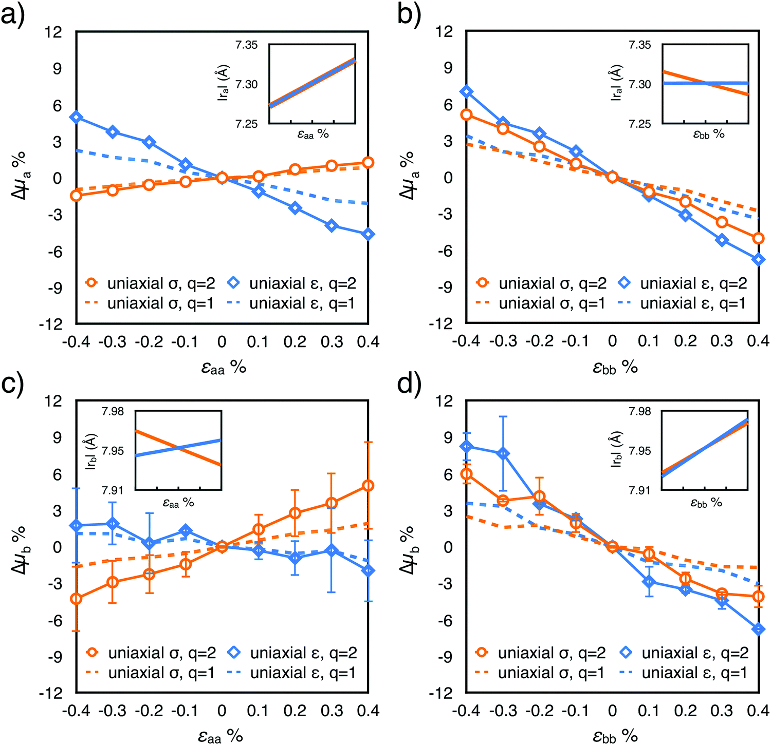 | ||
| Fig. 2 Relative mobility variations Δμi as a function of strain, calculated along the i = a (a and b panels) and b (c and d panels) crystal axes. The dashed and full lines refer to the two different models for charge transport considered (q = 1 for band-like transport and q = 2 for hopping, respectively). Insets: Variation of intermolecular distances |ra| and |rb| between dimers along the same direction of the calculated mobility variation, as a function of strain. Error bars were estimated as the difference between the mobility parallel to the cell vectors and with a misalignment of 5° and are negligible for plots (a) and (b). Relative mobilities calculated along the out-of-plane direction c are reported in Fig. S7 and S8 (ESI†). | ||
Uniaxial strain and uniaxial stress conditions result in striking differences, albeit in both cases the response is linear in the considered strain interval, and antisymmetric for tensile or compressive strains. Let us first consider the relative variation of mobility measured along the higher mobility axis, a, arising from the strain along the same axis. For uniaxial strain and uniaxial stress conditions, two opposite trends are observed (Fig. 2a). When uniaxial strain is applied along a, Δμa decreases by about 5% for a tensile strain of 0.4%. This trend alone can be easily rationalized by taking into account the change in the intermolecular distances ra and rb, since the electronic coupling (here Ja) is known to decrease exponentially with the increase of the intermolecular distance.27,53 Unexpectedly, when uniaxial stress conditions are applied (orange circles in Fig. 2a), Δμa is found to increase slightly with tension, yielding a positive mij coefficient which cannot be related to the changes in the intermolecular distances along a, as their average values along this direction are unchanged with respect to the uniaxial strain case (see Fig. 1c). The trend is not repeated when the strain is applied along b (Fig. 2b): in this case the two deformations have a very similar effect on Δμa, with the expected decreasing profile at increasing strain (positive values of mij). As for the mobility probed along the second in-plane direction b, for deformations along a and b, (Δμb in Fig. 2c and d) it follows qualitatively the same trend of the mobility along a.
For our system, we ruled out a major role of the fluctuations in intermolecular distances (recently suggested for explaining the increase of charge carrier mobility of a naphthobenzodithiophene upon compressive strain17) since the standard deviations of |ra|, |rb| and |rc| vary less than 1% in the considered strain interval (Fig. S2, ESI†). To fully understand the effect of the intermolecular fluctuations on the modulation of the transfer integral, it is useful to verify the values of the parameter ηi = Ji/si in the absence of strain, where si is the standard deviation of the Ji distribution, and as usual i = a, b, c. The smaller the value of η, the higher the impact of lattice dynamics on the transfer integral values.54–56 The three rubrene nearest neighbours are characterized by three distinct values of η: from our calculations they are 3.4, 2.0 and 1.6 for dimers along a, b and c respectively. All of them are large enough to indicate a weak or negligible dependence of the mobility on the amplitude of intermolecular vibrations, hence it is not expected that a strain-induced variation of si could significantly affect mobility values. In addition, we verified that imposing strain on the rubrene crystal does not modify this picture, since η changes very little upon strain (see Table S4, ESI†). As highlighted in Fig. 3, the variation of the average values of Ji actually originates from a shift of the whole distribution rather than a broadening (see also Fig. S7 and S8 and standard deviation and skewness values in Table S4, ESI†).
 | ||
| Fig. 3 Distributions of the absolute values of the instantaneous transfer integrals |Jta| and |Jtb| as a function of strain εii applied along the corresponding crystal axis: +0.4% (blue line), 0% (black line) and −0.4% (red line). (a) Uniaxial strain; (b) uniaxial stress conditions. Transfer integrals calculated along the out-of-plane direction c are reported in Fig. S7 (ESI†). | ||
2.3 Electromechanical response of rubrene single crystals
To further investigate the electromechanical response of rubrene, single crystals under mechanical strain were electrically characterized, in a transistor configuration, and the relative variations of drain-current with strain were compared to the calculated mobility changes discussed above. Different approaches exist to characterize the electrical properties of single crystals under stress and strain. The most common one uses flexible arrays of transistors, although new setups have recently appeared in the literature. For instance, Wu et al.23 measured the variations of rubrene work function by Kelvin probe force microscopy (KPFM) under different tensile strain by using thermal expansion of PDMS and silicon substrates. Here we apply a new method based on an Organic Field Effect Transistor (OFET) embedded in a suspended organic micro-cantilever, henceforth called cantiFETs, first described by Rao et al.35 and improved recently by Thuau et al., who fabricated highly sensitive electro-mechanical transducers using piezoelectrically-gated OFETs.37 In the present work, single crystal rubrene FETs are integrated in organic MEMS plastic cantilevers. By bending the flexible cantilever, controlled and uniform strains can be applied to the embedded transistors, thus enabling the accurate evaluation of the electromechanical properties of organic semiconductors (Fig. 4). The triangular shape is chosen to induce a uniform longitudinal stress in the crystal when a force is applied at the free-end of the cantilever.57 The rubrene crystal is positioned near the clamping region of the cantilever, in order to minimize bending-induced strain along the cantilever width direction (Fig. S10, ESI†). Then the applied force at the cantilever free-end induces uniaxial tensile strain in rubrene crystals along the cantilever length direction since in the width direction it is almost clamped. As a consequence, the intermolecular distance along a specific axis on rubrene single crystals is changed in a controllable fashion, as schematized in Fig. 4a. While monitoring the drain current of the transistor for different applied strain values, the electromechanical response of rubrene is characterized accurately and reversibly (Fig. 4d). | ||
| Fig. 4 Field effect transistors (FET) produced by lamination of single crystals on top of a cantilever beam (cantiFET), (a) 3D representation of a cantiFET. The top scheme represents the cantilever at rest, while at the bottom the cantilever is bent, inducing a uniaxial tensile strain along the b-axis of the crystal. (b) Architecture of the cantiFETs: a plastic substrate made of polyethylene naphthalate (PEN) is used as a support layer of the suspended cantilever. The integrated OFETs consist of an aluminum (AL) bottom gate electrode, a polystyrene (PS) gate dielectric, and gold (Au) source/drain top electrodes. (c) Typical forward and reverse transfer curve of a rubrene cantiFET at Vds = −50 V along the a-axis, recorded in the absence of strain. (d) Real time measurement of drain current along the b-axis in a device subjected to different tensile strains applied along the b-axis at Vds and Vgs equal to −50 V, showing the reversible behaviour of the cantiFET response. | ||
In practice, different mechanical and electrical configurations were tested experimentally, as shown in Fig. 5. Fig. 5 shows the results obtained for each device configuration: for all setups, the drain current, directly proportional to the mobility (see the ESI† for details), decreases when increasing tensile strain, as predicted by simulations in uniaxial strain conditions (cf.Fig. 2 and Table 2). The experimental results on the one hand validate the trends obtained by molecular dynamic simulations and, on the other hand, demonstrate the impact of strain on the mobility of rubrene using an original approach based on OFET-embedded MEMS configurations.
 | ||
| Fig. 5 Experimental relative variation of mobility as a function of strain magnitude and direction of application and measurement. Mobility variations were obtained assuming proportionality with drain current values in the saturation regime (see the ESI† for details). The inset pictures schematize the different setups: (a) strain applied along the a-axis and drain current measured along the same axis; (b) strain applied along b and current measured along a; (c) strain applied along a and current measured along b; (d) strain applied along b and current measured along b. Horizontal error bars represent the standard deviation on the determination of strain from the deflection profiles, while vertical error bars correspond to the standard deviation of the current calculated over three repeated measurement cycles. | ||
3. Discussion and conclusions
Controlled uniaxial tensile strain is applied to rubrene single crystals, simultaneously measuring the induced variation of current, using an original setup based on an organic field effect transistor embedded in a suspended polymeric micro-cantilever37 (Fig. 4a and b). Considering its reduced cost and ease of fabrication, this setup represents an excellent mechanical platform to characterise accurately the electrical properties of organic materials. Contrary to previous reports of an elastic-to-plastic transition occurring via thermal expansion on a poly(dimethylsiloxane) substrate at a strain of 0.05%,29 the registered response is elastic and reversible in the strain range considered (up to 0.18%, Fig. 4d). Quantitatively, the relative variation of current is negative, coherent with recent experiments exploiting wrinkling instabilities,15 and more pronounced when measured along the b-axis (Fig. 5b and d) than along the a-axis (the direction of higher mobility) (Fig. 5a and c). Interestingly, the effect is qualitatively independent of the direction of the application of the strain, revealing a strong coupling between the two in-plane directions of rubrene crystals and a microscopic mechanism more elaborate than the mere reduction of the electronic couplings caused by the increase of the intermolecular distances along the direction of application of strain. Rubrene crystals then appear to be more sensitive to strain when compared to TIPS-pentacene58 or alkylthiophenes,17 as suggested by their higher electromechanical sensitivity and stiffness.The variation of charge carrier mobility as a function of compressive and tensile strain is predicted by calculations combining molecular dynamics, quantum chemistry, and charge diffusion models. The computational results are validated through the comparison of the stiffness tensor with previously published experimental and theoretical data39,40 (Table 1), notably indicating negative Poisson's ratios when stress and strain couple the a and c (out-of plane) crystal axes. The relative mobility changes under uniaxial strain conditions, calculated assuming incoherent transport (Fig. 2, blue lines, q = 2) match semi-quantitatively with measurements, with larger electromechanical sensitivities when strain is applied along the b-axis (∼20) with respect to the a-axis (∼10), independent of the direction of the measurement of the current (see Table 2). Taking into consideration the possibility of coherent transport (dotted lines in Fig. 2) yields as expected a reduced response to strain, that does not alter the qualitative picture and still captures the correct order of magnitude of the experimental mobility variations.
The calculations extend the scope of the OFET experiments by considering also the conditions of uniaxial stress, corresponding to an ideal case in which the two dimensions of the crystal perpendicular to the applied stress direction are let free to adapt so as to minimize lateral stresses according to the corresponding Poisson's ratios (Fig. 1c). While the predicted change in mobility is very similar for uniaxial stress and uniaxial strain applied along b (Fig. 2c and d), quite surprisingly the response changes in sign for uniaxial stress along a, i.e. the mobility increases for tensile strains and decreases for compressive strains (Fig. 2a and c), despite intermolecular distances behaving oppositely. This result underlines the importance of considering the exact mechanical setup in interpretation of electro-mechanical experiments, because (i) the effect of mechanical deformation might not always be readily translated into a predictable mobility change, and (ii) the actual conditions of the experiment, such as the substrate mechanical properties, adhesive behaviour, or clamping, might strongly affect the magnitude and sign of the electrical response of the device.
Concerning the microscopic nature of the electrical response, for rubrene it originates from the shift of the whole electronic coupling distribution upon strain (Fig. 3), and not from a change in their standard deviation caused by the suppression or enhancement of intermolecular vibrations as recently put forward for explaining strain-mobility trends for a benzodithiophene derivative.17 Despite the strong dependence of the electronic coupling on the intermolecular distances, their variation alone is sufficient to rationalize the electric response only for uniaxial strain conditions, and not for uniaxial stress ones. In the latter case, although the unambiguous variation of mobility is clearly generated by the rearrangement of the molecules upon strain, it appears to be the complex result of tiny yet collective variations of several inter/intra-molecular parameters that influence the electronic couplings and ultimately, the measured current.
In summary, a systematic study of the electromechanical response of rubrene crystals under strain has been carried out. The results show a considerable agreement between the mobilities calculated under uniaxial strain conditions, and the measured current changes in the cantiFETs upon controlled strain. The anisotropy of the rubrene crystal structure translates into an anisotropy in its strain response, and remarkably the strain applied along b has a major impact on mobility along the direction of fastest charge transport a, and vice versa, with larger effects when the mobility is measured along b. This investigation brings new fundamental understanding on the nature of rubrene electrical response upon device deformation, helping the realization of more efficient devices, and stimulating future investigations for a wide range of crystalline and amorphous organic semiconductors.
4. Materials and methods
Computational details
The electronic couplings were calculated in the one electron approximation as J = 〈ϕAHOMO|H|ϕBHOMO〉, where A and B represent two adjacent rubrene molecules involved in the hole transfer, using the projective method at the ZINDO level of theory.31,53,59The average atomic positions of all dimers in the supercell were calculated every 100 ps over a MD production run of 10 ns, and their electronic couplings were averaged over the number of equivalent neighbours. This averaging over molecular vibrations allows for smooth trends versus strain and was used for producing Fig. 2. The relative magnitude of mobility along the crystal axis i = a, b, c is calculated at zero field and neglecting fluctuations of the ionization potential, by simultaneously taking into account the variations of transfer integrals and intermolecular distance vectors with strain:43,60
 | (1) |
 ,
,  is a cell axis unit vector, and μ0 is a constant, and q is an exponent that depends on the charge transport mechanism.
We considered two neighbours along a, four along b, and four along c. The second type of neighbours along c,43 was not considered throughout this study. The squared electronic coupling in eqn (1) is consistent both with a Marcus-like localized hopping regime and with a partially delocalized picture, more appropriate for the intralayer transport in the ab plane.52 The relative changes in mobility  were calculated using eqn (1)l along i = a, b, c and strains applied along j = a, b, c with respect to the same quantity at εjj = 0. The exponent q was set equal to 1 and 2, so as to encompass the expected behaviour of several transport mechanisms, and to let the reader easily guess the trends for other similar values of q which may appear in the different flavours of charge transport equations.46 Instantaneous transfer integrals Jt were also calculated for all dimers every 300 ps, and used to compute distributions as a function of strain (Fig. 3 and Fig. S7, S8, and averages |Jti| in Table S5, ESI†).
Preparation of rubrene single crystals
Rubrene crystals were grown using a physical vapour transport process. Commercial rubrene (Sigma-Aldrich) was placed inside a copper furnace as source material for crystal growth. Then, oxygen was removed from the furnace by means of Argon purge. The as-received rubrene was purified two times through physical vapour transport with an Argon flow of 30 ml min−1 and a heating temperature of 320 °C. Crystals were grown for several days before being collected and placed again in the same furnace, cleaned with isopropanol. In the third step, crystals were grown inside a glass furnace with an Argon flow of 15 ml min−1 and a heating temperature of 320 °C. The growth time was between 20 and 40 min in total, starting from room temperature. Crystals were collected and laminated manually on the cantilever using Microtools tips from MiTeGen, controlling the orientation of the crystal axes with respect to the electrodes. Only ultra-thin rubrene crystals with a thickness below 1 μm were used, since thicker crystals would otherwise delaminate from the substrate upon bending, owing to their higher rigidity.MEMS cantilever
Polyethylene naphthalate (PEN) square substrates of 2.25 cm2 and 50 μm-thick were patterned by xurography and cleaned in successive ultrasonic baths for 5 min each time (soaped water, deionized water, acetone, ethanol, isopropanol and deionized water). Then PEN substrates were thermally annealed at 180 °C for 2 hours. This curing allows the release of oligomers present on formation of the plastic surfaces. Aluminium was evaporated on PEN through shadow masks using an e-beam process so as to form the gate electrode (80 nm thick). Evaporation was performed under 1 × 10⁻⁶ mbar vacuum, with a deposition rate of 0.1 nm s−1. To spin coat the polystyrene (PS) gate dielectric layer, a solution was prepared by dissolving PS (280![[thin space (1/6-em)]](https://www.rsc.org/images/entities/char_2009.gif) 000 g mol−1) into chlorobenzene at a concentration of 70 mg mL−1. The solution was stirred overnight before being filtered (PTFE 0.45 μm). 120 μL of PS was then spin coated (20 s at 500 rpm then 60 s at 2000 rpm) to obtain a 1.7 μm-thick gate dielectric layer. Right after the spin coating, each sample was annealed on a hot plate at 80 °C during 5 hours under vacuum. Then gold electrodes (60 nm thick) were deposited through shadow masks via thermal evaporation, with a deposition rate of 0.1 nm s−1 under 5 × 10⁻⁶ mbar vacuum, to pattern the source/drain electrodes. Finally, the triangular shape of the cantilevers was patterned by xurography. On top of this architecture, rubrene single crystals were laminated manually between gold electrodes, in order to control their orientation. The channel length L = 50 μm of the cantiFET coincides with the distance between the gold electrodes, while the width of the contact varies from crystal to crystal (120–750 μm).
000 g mol−1) into chlorobenzene at a concentration of 70 mg mL−1. The solution was stirred overnight before being filtered (PTFE 0.45 μm). 120 μL of PS was then spin coated (20 s at 500 rpm then 60 s at 2000 rpm) to obtain a 1.7 μm-thick gate dielectric layer. Right after the spin coating, each sample was annealed on a hot plate at 80 °C during 5 hours under vacuum. Then gold electrodes (60 nm thick) were deposited through shadow masks via thermal evaporation, with a deposition rate of 0.1 nm s−1 under 5 × 10⁻⁶ mbar vacuum, to pattern the source/drain electrodes. Finally, the triangular shape of the cantilevers was patterned by xurography. On top of this architecture, rubrene single crystals were laminated manually between gold electrodes, in order to control their orientation. The channel length L = 50 μm of the cantiFET coincides with the distance between the gold electrodes, while the width of the contact varies from crystal to crystal (120–750 μm).
The cantiFETs were first characterized electrically in the absence of strain. In particular, the transfer curves of the transistors were obtained by applying Vds = 50 V, with a typical example shown in Fig. 4c. The transistors showed hole mobilities in the range of 1.1 cm2 V−1 s−1, an ION/IOFF ratio of up to 106, and threshold voltages Vth ranging from 0 to −30 V. A vertical force was applied to the cantilever tip using a micromanipulator (MiBot from Imina Technologies SA, Fig. S11, ESI†). The deflection δ was obtained by measuring the position of the cantilever extremity from the video recording (Navitar camera). The corresponding strain on the top surface is then calculated as ε = hδ/Λ2, where h and Λ are respectively the thickness and the length of the cantilever.
As the applied strain was kept below 0.2% to ensure elastic deformation of the rubrene crystals, and in agreement with the theoretical predictions of variation of mobility of only a few percent, transfer curves did not show enough significant changes to accurately characterize the electromechanical behaviour of rubrene (cf. Fig. S12, ESI†). Instead of using the full transfer curve, we then monitored the real-time value of the drain current in the saturation regime, with Vgs and Vds equal to −50 V. Every ten seconds, a tensile strain was applied to the cantilevers, reaching a maximum value of 0.18% before the strain was released gradually (Fig. 4d). To account for the time drift of the drain current at each value of strain (see Fig. 4b), the baseline was corrected with a quadratic function.
Conflicts of interest
There are no conflicts of interest to declare.Acknowledgements
This work in Bordeaux was funded by the French State grant ANR-10-LABX-0042-AMADEus managed by the French National Research Agency under the initiative of excellence IdEx Bordeaux program (reference ANR-10-IDEX-0003-02). We thank Dr Jérôme Cornil (UMons & FNRS, Belgium) for stimulating discussions.Notes and references
- Y. Qian, X. Zhang, L. Xie, D. Qi, B. K. Chandran, X. Chen and W. Huang, Adv. Mater., 2016, 28, 9243–9265 CrossRef CAS PubMed.
- H. Wang, X. Ma and Y. Hao, Adv. Mater. Interfaces, 2017, 4, 1600709 CrossRef.
- T. Q. Trung and N.-E. E. Lee, Adv. Mater., 2017, 29, 1603167 CrossRef PubMed.
- T. Someya, Z. Bao and G. G. Malliaras, Nature, 2016, 540, 379–385 CrossRef CAS PubMed.
- A. Chortos and Z. Bao, Mater. Today, 2014, 17, 321–331 CrossRef CAS.
- N. Muralidharan, R. Carter, L. Oakes, A. P. Cohn and C. L. Pint, Sci. Rep., 2016, 6, 27542 CrossRef CAS PubMed.
- M. H. Dahan and M. C. Toroker, J. Phys. Chem. C, 2017, 121, 6120–6125 CAS.
- P. Heremans, A. K. Tripathi, A. de Jamblinne de Meux, E. C. P. Smits, B. Hou, G. Pourtois and G. H. Gelinck, Adv. Mater., 2016, 28, 4266–4282 CrossRef CAS PubMed.
- S. Wagner and S. Bauer, MRS Bull., 2012, 37, 207–213 CrossRef.
- Y. Yao, H. Dong and W. Hu, Adv. Mater., 2016, 28, 4513–4523 CrossRef CAS PubMed.
- D. Käfer and G. Witte, Phys. Chem. Chem. Phys., 2005, 7, 2850 RSC.
- M. El Helou, O. Medenbach and G. Witte, Cryst. Growth Des., 2010, 10, 3496–3501 CAS.
- V. Podzorov, E. Menard, A. Borissov, V. Kiryukhin, J. A. Rogers and M. E. Gershenson, Phys. Rev. Lett., 2004, 93, 1–4 CrossRef PubMed.
- A. L. Briseno, R. J. Tseng, M.-M. Ling, E. H. L. Falcao, Y. Yang, F. Wudl and Z. Bao, Adv. Mater., 2006, 18, 2320–2324 CrossRef CAS.
- M. A. Reyes-Martinez, A. J. Crosby and A. L. Briseno, Nat. Commun., 2015, 6, 6948 CrossRef CAS PubMed.
- T. Morf, T. Mathis and B. Batlogg, 2016, arXiv:1606.06875v2.
- T. Kubo, R. Häusermann, J. Tsurumi, J. Soeda, Y. Okada, Y. Yamashita, N. Akamatsu, A. Shishido, C. Mitsui, T. Okamoto, S. Yanagisawa, H. Matsui and J. Takeya, Nat. Commun., 2016, 7, 11156 CrossRef CAS PubMed.
- Y. Esaki, T. Matsushima and C. Adachi, Adv. Funct. Mater., 2016, 26, 2940–2949 CrossRef CAS.
- M. Oehzelt, A. Aichholzer, R. Resel, G. Heimel, E. Venuti and R. G. Della Valle, Phys. Rev. B: Condens. Matter Mater. Phys., 2006, 74, 1–7 CrossRef.
- Z. Rang, M. I. Nathan, P. P. Ruden, V. Podzorov, M. E. Gershenson, C. R. Newman and C. D. Frisbie, Appl. Phys. Lett., 2005, 86, 1–3 CrossRef.
- K. Sakai, Y. Okada, S. Kitaoka, J. Tsurumi, Y. Ohishi, A. Fujiwara, K. Takimiya and J. Takeya, Phys. Rev. Lett., 2013, 110, 1–5 CrossRef PubMed.
- A. Jedaa and M. Halik, Appl. Phys. Lett., 2009, 95, 103309 CrossRef.
- A. N. Sokolov, Y. Cao, O. B. Johnson and Z. Bao, Adv. Funct. Mater., 2012, 22, 175–183 CrossRef CAS.
- G. Giri, E. Verploegen, S. C. B. Mannsfeld, S. Atahan-Evrenk, D. H. Kim, S. Y. Lee, H. Becerril, A. Aspuru-Guzik, M. F. Toney and Z. Bao, Nature, 2011, 480, 504–508 CrossRef CAS PubMed.
- H. T. Yi, M. M. Payne, J. E. Anthony and V. Podzorov, Nat. Commun., 2012, 3, 1259 CrossRef PubMed.
- V. Raghuwanshi, D. Bharti and S. P. Tiwari, Org. Electron., 2016, 31, 177–182 CrossRef CAS.
- Y. Park, K. S. Park, B. Jun, Y.-E. K. Lee, S. U. Lee and M. M. Sung, Chem. Mater., 2017, 29, 4072–4079 CrossRef CAS.
- X. Zheng, H. Geng, Y. Yi, Q. Li, Y. Jiang, D. Wang and Z. Shuai, Adv. Funct. Mater., 2014, 24, 5531–5540 CrossRef CAS.
- Y. Wu, A. R. Chew, G. A. Rojas, G. Sini, G. Haugstad, A. Belianinov, S. V. Kalinin, H. Li, C. Risko, J.-L. Brédas, A. Salleo and C. D. Frisbie, Nat. Commun., 2016, 7, 10270 CrossRef CAS PubMed.
- T. Cramer, L. Travaglini, S. Lai, L. Patruno, S. de Miranda, A. Bonfiglio, P. Cosseddu and B. Fraboni, Sci. Rep., 2016, 6, 38203 CrossRef CAS PubMed.
- L. Wang, G. Nan, X. Yang, Q. Peng, Q. Li and Z. Shuai, Chem. Soc. Rev., 2010, 39, 423–434 RSC.
- P. Cosseddu, G. Tiddia, S. Milita and A. Bonfiglio, Org. Electron., 2013, 14, 206–211 CrossRef CAS.
- V. Scenev, P. Cosseddu, A. Bonfiglio, I. Salzmann, N. Severin, M. Oehzelt, N. Koch and J. P. Rabe, Org. Electron. Phys., Mater. Appl., 2013, 14, 1323–1329 CrossRef CAS.
- B. Fraboni, A. Fraleoni-Morgera, Y. Geerts, A. Morpurgo and V. Podzorov, Adv. Funct. Mater., 2016, 26, 2229–2232 CrossRef CAS.
- V. Seena, A. Nigam, P. Pant, S. Mukherji and V. R. Rao, J. Microelectromech. Syst., 2012, 21, 294–301 CrossRef CAS.
- C. Ayela, G. Dubourg, C. Pellet and K. Haupt, Adv. Mater., 2014, 26, 5876–5879 CrossRef CAS PubMed.
- D. Thuau, M. Abbas, G. Wantz, L. Hirsch, I. Dufour and C. Ayela, Sci. Rep., 2016, 6, 38672 CrossRef CAS PubMed.
- D. Tank, H. H. Lee and D. Y. Khang, Macromolecules, 2009, 42, 7079–7083 CrossRef.
- M. A. Reyes-Martinez, A. Ramasubramaniam, A. L. Briseno and A. J. Crosby, Adv. Mater., 2012, 24, 5548–5552 CrossRef CAS PubMed.
- Y. Zhang, D. R. Manke, S. Sharifzadeh, A. L. Briseno, A. Ramasubramaniam and K. J. Koski, Appl. Phys. Lett., 2017, 110, 71903 CrossRef.
- V. C. Sundar, J. Zaumseil, V. Podzorov, E. Menard, R. L. Willett, T. Someya, M. E. Gershenson and J. A. Rogers, Science, 2004, 303, 1644–1646 CrossRef CAS PubMed.
- M. M. Ling, C. Reese, A. L. Briseno and Z. Bao, Synth. Met., 2007, 157, 257–260 CrossRef CAS.
- V. Stehr, J. Pfister, R. F. Fink, B. Engels and C. Deibel, Phys. Rev. B: Condens. Matter Mater. Phys., 2011, 83, 155208 CrossRef.
- T. J. Pundsack, N. O. Haugen, L. R. Johnstone, C. D. Frisbie and R. L. Lidberg, Appl. Phys. Lett., 2015, 106, 113301 CrossRef.
- A. Troisi, Adv. Mater., 2007, 19, 2000–2004 CrossRef CAS.
- S. Fratini, D. Mayou and S. Ciuchi, Adv. Funct. Mater., 2016, 26, 2292–2315 CrossRef CAS.
- S. Fratini, S. Ciuchi, D. Mayou, G. T. de Laissardiere and A. Troisi, Nat. Mater., 2017, 16, 998–1002 CrossRef CAS PubMed.
- C. Liu, K. Huang, W.-T. Park, M. Li, T. Yang, X. Liu, L. Liang, T. Minari and Y.-Y. Noh, Mater. Horiz., 2017, 4, 608–618 RSC.
- A. Troisi, J. Chem. Phys., 2011, 134, 34702 CrossRef PubMed.
- G. Nan, X. Yang, L. Wang, Z. Shuai and Y. Zhao, Phys. Rev. B: Condens. Matter Mater. Phys., 2009, 79, 1–9 CrossRef.
- T. Vehoff, B. Baumeier, A. Troisi and D. Andrienko, J. Am. Chem. Soc., 2010, 132, 11702–11708 CrossRef CAS PubMed.
- B. Blülle, A. Troisi, R. Häusermann and B. Batlogg, Phys. Rev. B: Condens. Matter Mater. Phys., 2016, 93, 35205 CrossRef.
- V. Coropceanu, J. Cornil, D. A. da Silva Filho, Y. Olivier, R. Silbey and J.-L. Brédas, Chem. Rev., 2007, 107, 926–952 CrossRef CAS PubMed.
- N. G. Martinelli, Y. Olivier, S. Athanasopoulos, M. Ruiz Delgado, K. R. Pigg, D. A. Da Silva Filho, R. S. Sánchez Carrera, E. Venuti, R. G. Delia Valle, J. L. Brédas, D. Beljonne and J. Cornil, ChemPhysChem, 2009, 10, 2265–2273 CrossRef CAS PubMed.
- S. Illig, A. S. Eggeman, A. Troisi, L. Jiang, C. Warwick, M. Nikolka, G. Schweicher, S. G. Yeates, Y. H. Geerts, J. E. Anthony and H. Sirringhaus, Nat. Commun., 2016, 7, 10736 CrossRef CAS PubMed.
- Y. Tsutsui, G. Schweicher, B. Chattopadhyay, T. Sakurai, J. B. Arlin, C. Ruzié, A. Aliev, A. Ciesielski, S. Colella, A. R. Kennedy, V. Lemaur, Y. Olivier, R. Hadji, L. Sanguinet, F. Castet, S. Osella, D. Dudenko, D. Beljonne, J. Cornil, P. Samorì, S. Seki and Y. H. Geerts, Adv. Mater., 2016, 28, 7106–7114 CrossRef CAS PubMed.
- H. Nesser, C. Ayela, I. Dufour and H. Debéda, Flex. Print. Electron., 2017, 2, 15001 CrossRef.
- X. Zheng, H. Geng, Y. Yi, Q. Li, Y. Jiang, D. Wang and Z. Shuai, Adv. Funct. Mater., 2014, 24, 5531–5540 CrossRef CAS.
- I. Yavuz, B. N. Martin, J. Park and K. N. Houk, J. Am. Chem. Soc., 2015, 137, 2856–2866 CrossRef CAS PubMed.
- W. Deng and W. A. Goddard III, J. Phys. Chem. B, 2004, 108, 8614–8621 CrossRef CAS.
Footnote |
| † Electronic supplementary information (ESI) available. See DOI: 10.1039/c7mh00489c |
| This journal is © The Royal Society of Chemistry 2018 |