
Enhanced charge carrier mobility and lifetime suppress hysteresis and improve efficiency in planar perovskite solar cells†
Silver-Hamill
Turren-Cruz
 ab,
Michael
Saliba
*a,
Matthew T.
Mayer
a,
Hector
Juárez-Santiesteban
b,
Xavier
Mathew
c,
Lea
Nienhaus
d,
Wolfgang
Tress
a,
Matthew P.
Erodici
e,
Meng-Ju
Sher
e,
Moungi G.
Bawendi
d,
Michael
Grätzel
a,
Antonio
Abate
f,
Anders
Hagfeldt
*a and
Juan-Pablo
Correa-Baena
*ad
ab,
Michael
Saliba
*a,
Matthew T.
Mayer
a,
Hector
Juárez-Santiesteban
b,
Xavier
Mathew
c,
Lea
Nienhaus
d,
Wolfgang
Tress
a,
Matthew P.
Erodici
e,
Meng-Ju
Sher
e,
Moungi G.
Bawendi
d,
Michael
Grätzel
a,
Antonio
Abate
f,
Anders
Hagfeldt
*a and
Juan-Pablo
Correa-Baena
*ad
aÉcole Polytechnique Fédérale de Lausanne, Station 6, CH-1015-Lausanne, Switzerland. E-mail: Michael.saliba@epfl.ch; anders.hagfeldt@epfl.ch
bBenemérita Universidad Autónoma de Puebla. CIDS, Av. San Claudio y 18 Sur, Col. San Manuel, Ciudad Universitaria, CP 72570, P.O. Box 1067, Puebla, Pue. 7200, Mexico
cInstituto de Energías Renovables, Universidad Nacional Autónoma de México, Temixco, Morelos 62580, Mexico
dMassachusetts Institute of Technology, Cambridge, MA 02139, USA. E-mail: jpcorrea@mit.edu
eWesleyan University, Middletown, CT 06459, USA
fYoung Investigator Group Active Materials and Interfaces for Stable Perovskite Solar Cells, Helmholtz-Zentrum Berlin für Materialien und Energie, Kekuléstrasse 5, 12489 Berlin, Germany
First published on 5th December 2017
Abstract
Perovskite solar cells (PSCs) are very promising lab-scale technologies to deliver inexpensive solar electricity. Low-temperature, planar PSCs are of particularly interest for large-scale deployment due to their inherent suitability for flexible substrates and potential for silicon/perovskite tandems. So far, planar PSCs have been prone to large current–voltage hysteresis and low stabilized power output due to a number of issues associated with this kind of device configuration. We find that the suppression of the yellow-phase impurity (∂-FAPbI3) present in formamidium-based perovskites, by RbI addition, contributes to low hysteresis, higher charge carrier mobility, long-lived carrier lifetimes and a champion stabilized power output of 20.3% using SnOx as the electron selective contact. We study the effects of these impurities on the transient behavior that defines hysteresis and its relation to ionic movement. In addition, we find that the formation of a RbPbI3 phase does not significantly affect the charge carrier lifetimes and consequently the performance of the devices. This brings new physical insights onto the role of different impurities in perovskite solar cells, which make these materials so remarkable.
Broader contextPerovskite-based solar cells have emerged as a promising technology for highly efficient and low-cost photovoltaics. High efficiencies so far reported go beyond 20% in mesoporous-based solar cells, but very few reports have shown this for the planar-based analogues. This is in part because planar perovskite solar cells have traditionally suffered from more pronounced hysteresis, detrimental to stabilized power output. In this work, we show that by improving the charge carrier mobilities and lifetimes, hysteresis is suppressed and open circuit voltages are improved. This translates into planar perovskite solar cells processed at low temperature and yielding efficiencies beyond 20%. This study sheds light on the importance of charge carrier mobility related to hysteresis, and therefore sets a pathway towards high efficiency planar perovskite solar cells. |
Introduction
In the last few years organic–inorganic hybrid perovskite solar cells (PSCs) have emerged as one of the most promising candidates for thin-film, low cost solar technologies.1 Perovskites used for photovoltaics (PV) have an AMX3 formula that is comprised of a monovalent cation, A = cesium (Cs+), methylammonium (MA); formamidinium (FA);2–7 a divalent metal M = (Pb2+; Sn2+);8–10 and a halide anion X = (Cl−, Br−; I−).11These materials exhibit high optical absorption coefficients12 and long charge carrier diffusion lengths in the μm-range.13,14 These properties have allowed the power conversion efficiency (PCE) of PSCs to jump from 3.8%15 in 2009 to 22.1%16,17 in 2016, which is unprecedented for any other PV material.18,19 Much excitement is also due to the possibility of processing perovskite materials by a large number of techniques ranging from spin coating,8 dip coating,20 2-step interdiffusion,21 to vacuum assisted evaporation.22 Most of these techniques are low temperature compatible (<100 °C) and can be solution-based. Therefore, PSCs are ideal for low-cost commercialization.
The highest reported efficiencies have been achieved with perovskites with mixed MA/FA cations and Br/I halides.4,23 Recently, Cs was used to explore more complex cation combinations, i.e. Cs/MA, Cs/FA and Cs/MA/FA.7,24–27 Similarly, Rb was added into a multication perovskite, showing improved efficiency and long-term device stability at elevated temperatures of 85 °C measured by maximum power point tracking (MPPT).28
Currently, the main device architectures investigated in PSCs are the mesoporous TiO2-infiltrated and the planar (mesoporous-free) configuration. Recently, we have shown that planar MA/FA, Br/I perovskites using an atomic layer deposited (ALD) SnOx electron selective layer yield stabilized efficiencies of 19.5%.29,30 The low-temperature processing enabled a monolithic silicon/perovskite tandem device with a perovskite top-cell processed on a temperature sensitive silicon bottom-cell.31 We replaced the ALD processing with a low-temperature, solution-processed deposition of SnOx resulting in efficiencies of close to 21% putting the planar architecture on par with the mesoporous counterpart.32 More recently, planar PSCs with a modified low-temperature TiO2 also achieved efficiencies of around 21%.33 Even though solution-processing of metal oxides is useful for single-junction device upscaling, ALD is an ideal technique for manufacturing tandem devices31,34 involving perovskites which are sensitive to polar solvents.
One of the roadblocks limiting overall efficiency is the open-circuit voltage (VOC), which can be improved by more conformal charge selective and photoactive layers.29–31,35–37 In addition, it has been shown that improving the perovskite crystal quality can also lead to improved VOC and therefore higher efficiencies.7,28 Crystal impurities are commonly found in FA-based perovskites where the more bulky cations tend to partially form a wide bandgap, layered “yellow” phase polymorph (∂-FAPbI3).
Here, we report on the suppression of hysteresis and the enhancement of carrier lifetimes and VOC due to phase impurity management. We suppress the ∂-FAPbI3 by adding only 1% of RbI to the precursor solution used to fabricate a mixed MA/FA/Pb/I/Br formulation that has reached efficiencies exceeding 18% for planar devices.30 This leads to improved carrier mobility, as measured by terahertz (THz) photoconductivity. In addition, Rb-containing samples show remarkable charge carrier lifetimes above 1 μs, higher open-circuit voltages and low current–voltage (J–V) hysteresis, when compared to samples with remnants of ∂-FAPbI3. A champion stabilized efficiency of 20.3% for SnOx-based planar PSCs is achieved; among the highest for this device configuration. Interestingly, the formation of photoinactive RbPbI3 (when using concentrations of 10% RbI) does not influence the open-circuit voltage. Therefore, this study sheds light on the role of phase impurities in charge carrier dynamics and device performance, which is imperative to going beyond state-of-the-art PSCs.
Results and discussion
We investigated a mixed ion perovskite based on a precursor solution with the formula Rbx(MA0.17FA0.83)(100−x)Pb(I0.83Br0.17)3, and added RbI from 1% to 10%. For brevity, we denote these compositions as RbxMAFA (x is a percentage of RbI added in solution). All preparation details are given in the materials and methods section.Film characterization
We investigated the introduction of RbI to the perovskite solution and its effect on crystal quality. In Fig. 1A and B, we show X-ray diffraction (XRD) data for RbxMAFA with x = 0, 1, 5, 10 mol%. All compositions exhibited a typical perovskite peak at ∼14° that corresponds to the (110)/(002) orientation of the photoactive black phase of the perovskite material. For MAFA additional peaks were found at 12.6° and at 11.6° corresponding to PbI2 and δ-FAPbI3, respectively. Upon addition of small amounts of Rb from 1, 5 to 10%, the yellow phase and the PbI2 peaks were suppressed. Similar recent reports have also shown this effect with Rb,38 and others with Cs.7 A small peak at 2-theta ∼10° is detected for Rb-containing samples, and can be attributed to the RbPbI3 compound.28 More detailed XRD spectra can be found in Fig. S1 (ESI†). Ultraviolet-visible (UV-vis) and photoluminescence (PL) spectroscopy was performed on all MAFA and RbxMAFA films as shown in Fig. 1C. All samples showed narrow PL peaks at ∼770 nm, with a small red-shift for Rb10. Absorption onset also showed red shifting for the 10% Rb samples. In our recent work we showed how introduction of Rb can affect the composition of the crystal in the bulk.39 The compositional change can then lead to different bandgap formation. | ||
| Fig. 1 XRD and optical characterization of RbxMAFA compounds. (A) XRD spectra for RbxMAFA series and the RbPbI3 reference, and (B) the 2-theta details from 9° to 16°, XRD of perovskite films with the main peaks. (C) UV-vis (line-symbol) and photoluminescence (solid lines) spectra for all samples. (D) Photographs of samples without and with Rb addition (from left to right 0, 1, 5, 10%), and no heat treatment, to show the effect RbI addition has on crystallization at room temperature. | ||
The addition of the RbI in the MAFA solution leads to a lowering of the average RbxMAFA cation radius allowing the incorporation of cations that were considered too small previously.7,28 The black phase is entropically stabilized even at room temperature, resulting in a suppression of the hexagonal ∂-FAPbI3 perovskite. With the addition of RbI, a visible black-phase perovskite is induced upon antisolvent quenching and without heat treatment (Fig. 1D). RbI addition is therefore able to induce the black (cubic) perovskite crystallization without the need of heat treatment, similar to the effect of Cs.40
We investigated the morphological changes upon addition of RbI, as shown in Fig. 2. Top-view scanning electron microscopy (SEM) images of perovskite films with 0, 1, 5 and 10% of Rb are shown as A, B, C and D, respectively. As the Rb content is increased, the grain size slightly increases. The MAFA composition shows a crystal size average of 307 nm distributed on the film surface. With the addition of 1% of Rb in MAFA we see an increased grain size by 70 nm to an average of 381 nm, with small crystallites embedded in larger ones, compared with the MAFA controls. Addition of 5 and 10% of RbI increased average grain size to 433 and 452 nm, respectively, and small crystallites (seen in samples 0 and 1% RbI) are suppressed. The grain size change is rather small. However, it has been shown that larger grains are beneficial for charge transport and improved device performance.29,36,41 All the grain size distributions are shown in Fig. S2 (ESI†).
 | ||
| Fig. 2 The effect of RbI addition on perovskite morphology. Scanning electron micrographs for perovskites based on (A) Rb0MAFA, (B) Rb1MAFA, (C) Rb5MAFA, and (C) Rb10MAFA, scale bar in all SEM images is 400 nm. | ||
Solar cell performance metrics
A schematic and a cross-sectional scanning electron microscopy image of a complete solar cell is shown in Fig. 3A and B, respectively. The solar cell structure used is a stack of glass/fluorine-doped tin oxide (FTO)/SnOx/perovskite/spiro-OMeTAD/gold. Compatible with Si/perovskite tandems, the 15 nm of SnOx as the electron selective layer, is deposited by ALD. The perovskite and hole selective layers (spiro-OMeTAD) are 500 nm and 200 nm thick, respectively. An 80 nm gold layer is thermally evaporated as the top electrode.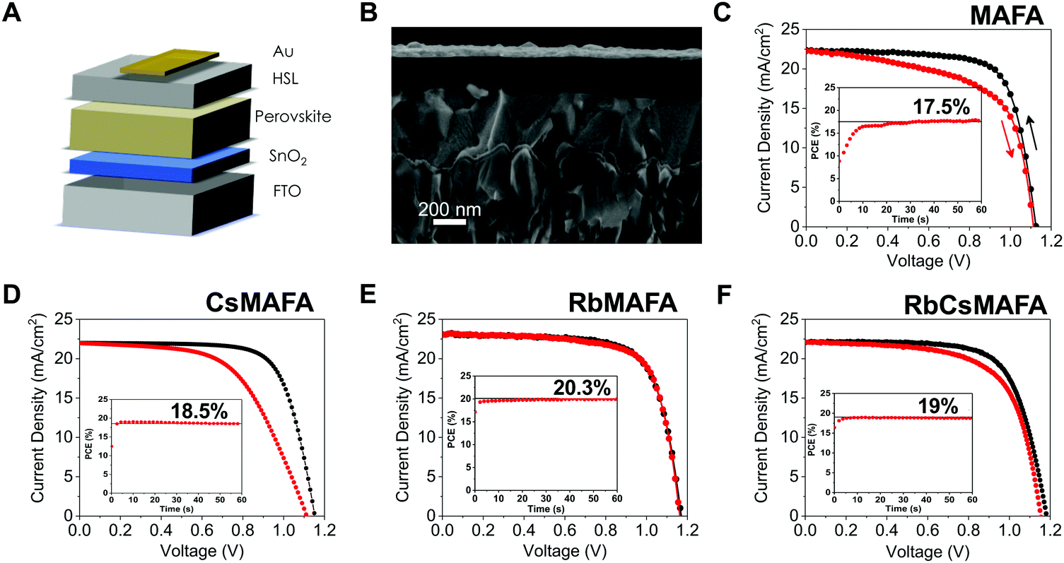 | ||
| Fig. 3 Performance metrics of planar perovskite solar cells based on different compositions. (A) Schematic and, (B) cross-sectional SEM of a typical planar perovskite solar cell FTO/SnOx/perovskite/spiro-MeOTAD/gold. (C) Current density–voltage characteristics for a PSC without Rb or Cs, (D) with 5% Cs in MAFA, (E) the champion PSC with 1% of Rb in MAFA and (F) with 5% Rb, 5% Cs in MAFA. All solar cells were measured at a scan rate of 10 mV s−1 and AM 1.5 G illumination with light intensity of 100 mW cm−2. Insets are the maximum power point tracking for each device and an active area for each pixel of 0.16 cm2. For statistics on all of these compositions see Fig. S3 and S4 (ESI†). | ||
The photovoltaic characteristics of the best PSCs for MAFA is plotted in Fig. 3C, where devices yielded 17.5% by MPPT, similar to earlier reports on ALD SnOx planar PSCs with that same composition.30 Large hysteresis is prevalent in the current–voltage curves. Upon addition of 5% Cs into the MAFA perovskite, the VOC is increased slightly as is the efficiency, which reaches 18.5% by MPPT (Fig. 3D), similar to the stabilized 19% obtained in our earlier work.32 Interestingly, no major difference is observed in hysteresis with the addition of Cs. We note that we showed similar behavior in our earlier study, if slightly less hysteretic, where a combination of ALD SnOx and CsMAFA also yielded relatively high hysteresis. Higher stabilized efficiencies for Rb-added samples were achieved, where the champion device yielded 20.3% for samples with 1% Rb (Fig. 3E) and 19% for samples with 5% Rb and 5% Cs in the MAFA mixtures (Fig. 3F).
The J–V characteristics for the 1% Rb show a high open circuit voltage of 1.17 V, a current density of 23.1 mA cm−2 (using an antireflective coating) and a very low hysteresis. We note that these devices are measured 1 or 2 days after preparation. In our previous work,30 we reported that in order to achieve the highest hysteresis-free efficiency, the samples were measured after 1 week or longer. Surprisingly, by adding only 1% Rb, the samples show significantly reduced hysteresis conditions without the time delay of days that is characteristic for MAFA perovskites.
While this work is based mostly on planar PSCs with SnOx selective contacts by ALD, we also prepared devices using a combination of spin-coating (SC) and chemical bath deposition (CBD), to understand the interactions of the contact and the perovskite composition.32 In our previous work we used CsMAFA perovskites as the photoabsorber and here, in an attempt to understand the role of Rb in other planar PSCs, we compare both SnOx deposition methods. Similar to the Rb effect in ALD SnOx, hysteresis is significantly changed upon addition of Rb to MAFA in SC-CBD-based devices (Fig. S3, ESI†). One important thing to note, is that the morphology of SnOx is very different depending on deposition method. While SnOx by ALD makes a smooth and conformal layer, by SC-CBD, the layer is rougher.30,32 Moreover, as we have reported, hysteresis can be affected by time scale,42 morphological features,36 energetics,30 and recombination.43 For that reason, we focus on the hysteresis behavior using only ALD as a highly controlled deposition technique, to avoid creating additional effects.
Photovoltaic parameters (more than 60 devices were made in total) for all compositions, using ALD, are shown in Fig. S4 (ESI†). We can observe that the VOC, JSC, and PCE increase when adding Cs to MAFA, and further when adding Rb to the CsMAFA perovskite. The addition of Rb to MAFA sees similar response to that of RbCsMAFA, regardless of the concentration of Rb introduced (up to 10% in solution). The increase in JSC can be attributed to the hysteresis effect, where scan rate can determine its magnitude, as has been shown in other works.29,35,36 Fill factor variations are difficult to assess due to severe changes between the backward and forward scan (hysteresis effect; the dependence of FF on scan rate in Fig. 4D and E). Interestingly, the formation of wider bandgap and layered RbPbI3 phase is not shown to significantly change recombination dynamics, and by proxy the VOC. On the other hand, the suppression of PbI2 and ∂-FAPbI3 impurities allows for higher VOC.
 | ||
| Fig. 4 Study of hysteresis for devices fabricated with different perovskite compositions. (A) Statistically-significant hysteresis (defined as the difference in efficiency between the backward and forward scan) for devices with different compositions. Here devices with perovskites containing Rb vs. those containing no Rb, are highlighted. (B) Intensity modulated photocurrent spectroscopy in the imaginary part of the current response,36 where the low frequency feature is highlighted for its relation to ionic movement. Current–voltage curves at different scan speeds for devices. (C) Effective THz carrier mobility for perovskite films on quartz slides. (D) Current–voltage plots at different scan rates without and (E) with 1% Rb. | ||
Hysteresis
To establish that Rb has such a significant effect on hysteresis and Cs alone does not, we collected over 60 device hysteresis metrics (Fig. 4A), defined as the difference in efficiency between the backward and forward scan. In Fig. S5 (ESI†), we show that although Rb concentration has a relatively small effect on the backward scan of statistically-significant device metrics, it does have a large effect on the stabilized efficiencies. This also exemplifies the need to use MPPT to measure devices, in addition to the ubiquitous J–V curve.We investigated the transient phenomena that define hysteresis. First, we measure the effect of RbI addition on the movement of ions. Fig. 4B presents the imaginary part of the current response to the intensity modulated photocurrent (IMPS) of devices with 1% and without RbI. The measurement shows that the slow component in the 0.1–100 Hz range is present for both types of devices. We attribute this to a response to light modulation which is due to ionic movement within the perovskite and it is in good agreement with our earlier work.36 This slow time component is strongly tied to hysteresis and it was shown that faster response (i.e. higher frequency) to light modulation is a sign of faster equilibration currents and therefore J–V hysteresis is unlikely to be detected at the scan speed typically used (10 mV s−1). From this analysis, devices with only 1% of RbI are expected to exhibit minimal hysteresis compared to the MAFA analogues.
We measured the effects of RbI addition to the charge carrier mobilities of the studied perovskites. We know that in PSCs, the electric field distribution is influenced by intrinsic mobile ionic defects, such as I vacancies, which tend to screen the electric field by accumulating at interfaces. Low carrier mobility causes ionic defects to respond slowly to voltage changes and are believed to be responsible for the hysteresis.42,44,45 The hysteresis occurs because the collection efficiency of photogenerated charge carriers is dependent on the applied voltage, and on the corresponding electric field. Therefore, hysteresis can be suppressed by increasing charge carrier mobility and extraction to make it less sensitive to the electric field.46 We studied the mobility of these perovskites with terahertz (THz) photoconductivity measurements. We found that charge carrier mobility increases with Rb concentration, which could also explain how devices reaches equilibrium currents faster and reduce hysteresis, as charges are collected faster than ions move. Fig. 4C shows effective charge carrier mobility results from 400 nm pump THz-probe transient photoconductivity measurements.47 Each 400 nm pump pulse excites n = 2 × 1019 cm−3 carriers in all samples. As the EQE (Fig. S6, ESI†) and absorption do not change with RbI addition (up to 5% Rb), and we obtain effective THz mobility by dividing measured photoconductivity (Δσ) by elementary charge q and n. The carrier mobility for Rb1MAFA improved by 8% with respect to Rb0MAFA. For Rb5MAFA, the carrier mobility increased even further by 25%, relative to Rb0MAFA. Additionally, the increased development of a photoinactive RbPbI3 phase (which appears at 1% RbI) did not seem to hinder the photoconductivity, at least up to 5% Rb. This increase in mobility could possibly be the result of increasingly larger grain size.
To further characterize and understand the changes in hysteresis we performed JV scans as a function of scan rate (Fig. 4D and E). We observe that the hysteresis increases for faster scans up to a certain scan rate before it decreases again, for the MAFA control, and it decreases regardless of scan rate for the RbMAFA device. This is consistent with previous studies, which explained this behavior with a characteristic response time of the slowly moving ions.42 Both, MAFA (Fig. 4D) and Rb1MAFA (Fig. 4E) devices show this trend, however on different time scales. Hysteresis is similarly pronounced for both systems when the scan is performed at 10 to 100 mV s−1 for MAFA and at 10![[thin space (1/6-em)]](https://www.rsc.org/images/entities/char_2009.gif) 000 mV s−1 for Rb1MAFA. This implies a response that is two to three orders of magnitude faster for the Rb1MAFA device, matching the results from IMPS (Fig. 4B). This trend in response time is also reflected in current transients obtained upon a voltage step from 0 or 1.15 V prebias to 1 V (Fig. S7, ESI†). Interestingly, instantaneously after switching the voltage from 0 to 1 V, the photocurrent is similarly low (almost 0), indicating that the ion distribution that was established at 0 V prebias affects both devices in the same way. However, the Rb1MAFA device reaches equilibrium currents much faster. Therefore, we conclude that addition of RbI, suppression of impurity phases and slightly larger grains allow for a fast redistribution of the ions and avoid unfavorable trapping of ionic charge, aided by the increase in mobility (Fig. 4C). This reduces hysteresis and allows for higher values of stabilized power.
000 mV s−1 for Rb1MAFA. This implies a response that is two to three orders of magnitude faster for the Rb1MAFA device, matching the results from IMPS (Fig. 4B). This trend in response time is also reflected in current transients obtained upon a voltage step from 0 or 1.15 V prebias to 1 V (Fig. S7, ESI†). Interestingly, instantaneously after switching the voltage from 0 to 1 V, the photocurrent is similarly low (almost 0), indicating that the ion distribution that was established at 0 V prebias affects both devices in the same way. However, the Rb1MAFA device reaches equilibrium currents much faster. Therefore, we conclude that addition of RbI, suppression of impurity phases and slightly larger grains allow for a fast redistribution of the ions and avoid unfavorable trapping of ionic charge, aided by the increase in mobility (Fig. 4C). This reduces hysteresis and allows for higher values of stabilized power.
Non-radiative recombination
With the addition of 1% or more RbI to the MAFA perovskite, a systematic increase in VOC was achieved. Fig. 5A shows the average and maximum VOC achieved for MAFA, 1%, 5%, and 10% RbI samples. With as little as 1% RbI, VOC increased by 15–20 mV. In Fig. 5B, all batches made with RbI showed higher VOC's compared with the MAFA controls, hinting at reduced non-radiative recombination. We performed time resolved photoluminescence (TRPL) studies to investigate the dynamics of recombination through lifetime of photoexcited carriers in the different materials (Fig. 5C). All compositions with RbI showed a long exponential PL decay tail with time constants above 1 μs, contrasting the short-lived traces for the MAFA reference yielding 0.55 μs (Table 1). This is in agreement with the higher voltages shown in Fig. 5A and B for the RbI-added samples. In addition to the increased lifetimes, we observed an increase in the number of detected photons, which is directly related to the radiative quantum yields of these materials, by a factor of 4, 12 and 17 for Rb1MAFA, Rb5MAFA, Rb10MAFA, respectively, when compared to Rb0MAFA (Table 1). Interestingly, the initial fast decay seems to follow a different trend. Samples with 1% RbI show a decrease of the quenched early time component, suggesting a more defect-free material than the original neat MAFA. This trend is reversed as RbI concentration is increased to 10% leading to further increase of quenching in this faster regime, without affecting the long-tail component. However, these early time dynamics do not appear to affect the VOC of the full devices significantly. We hypothesize that the δ-FAPbI3 is recombination active and drives the VOC down whereas the formation of the RbPbI3 phase (from XRD in Fig. 1) does not affect recombination significantly to dominate the change in VOC. | ||
| Fig. 5 Open-circuit voltage and charge carrier lifetimes (A). Average VOC for Rb0MAFA, Rb1MAFA, Rb5MAFA and Rb10MAFA and respective (B). VOC over six batches. (C) Time-resolved photoluminescence lifetimes for perovskite films on glass slides (measured through the glass side to avoid emission from air-exposed layers). | ||
| Sample | Total counts | Lifetime (μs) |
|---|---|---|
| Rb0MAFA | 1.48 × 10⁶ | 0.55 |
| Rb1MAFA | 6.35 × 10⁶ | 1.37 |
| Rb5MAFA | 1.79 × 10⁷ | 1.30 |
| Rb10MAFA | 2.56 × 10⁷ | 1.93 |
Conclusions
We have investigated the effects of RbI incorporation into a mixed ion perovskite solution containing FAPbI3 and MAPbBr3 (precursor solution composition of 83% and 17%, respectively). Addition of as little as 1% RbI in precursor solution, suppressed the yellow phase characteristic of FAPbI3, and the excess PbI2 found in the films. These improvements in the polycrystalline films led to significantly lower hysteresis for the Rb-containing films and higher stabilized efficiencies up to 20.35% for the 1% RbI samples. The mobility of the films was increased significantly, which we believe is instrumental for the suppression of hysteresis. In addition, the incorporation of RbI yielded longer charge carrier lifetimes and systematically higher VOC's. This work represents an important advancement in understanding and suppressing hysteresis to ultimately achieve planar perovskite solar cells beyond 21%.Materials and methods
Materials
All materials were purchased from Sigma-Aldrich and used as received, unless stated otherwise. The organic cation iodide salts were purchased from Dyesol; the lead compounds from TCI and the RbI from abcr GmbH.Lead halide perovskite precursor solutions
:DMSO 4:1 (v:v).
:99, 5:95 and 10:90, which is described in the text as 1%, 5% and 10%, respectively.
Solar cell preparation
:1) for 10 min. All substrates were further cleaned by UV-ozone for 15 min before deposition of SnO2.
Finally, 70–80 nm of gold top electrode was thermally evaporated under high vacuum.
Characterization
The solar cells were measured using a 450 W xenon light source (Oriel). A Schott K113 Tempax filter (Präzisions Glas & Optik GmbH) was used to reduce the spectral mismatches between AM 1.5G and the light source. A Si photodiode equipped with an IR-cutoff filter (KG3, Schott) was used as a reference. Current–voltage data were obtained by applying an external voltage bias and measuring the current response with a digital source meter (Keithley 2400). The voltage scan rate was set to 10 mV s−1. The photovoltaic data was collected without any device preconditioning, such as light soaking. In order to fix the active area of the devices and avoid artifacts produced by scattered light a black metal mask was used during the measurements. The IV data for champion devices gathered with antireflective coating on a 0.16 cm2 mask aperture whereas the data for the statistical analysis devices collected without antireflective coating.UV-vis measurements were performed on a Varian Cary 5. Scanning electron microscopy (SEM) was performed on a ZEISS Merlin HR-SEM. Secondary electron images were acquired with an EDX detector. X-ray powder diffractions (XRD) were recorded on an X’Pert MPD PRO (Panalytical) equipped with a ceramic tube (Cu anode, λ = 1.54060 Å), a secondary graphite (002) monochromator and a RTMS X’Celerator (Panalytical) in an angle range of 2θ = 5° to 60°. Photoluminescence spectra were obtained with Fluorolog 322 (Horiba Jobin Ybon Ltd) with the range of wavelength from 620 nm to 850 nm by exciting at 460 nm. The samples were mounted at 60° and the emission recorded at 90° from the incident beam path.
Transient PL lifetimes were obtained by time-correlated single photon counting (TCSPC). The sample was excited by a pulsed 405 nm wavelength laser (PicoQuant LDH-C 400) at an average incident power of 40 nW at a repetition rate of 200 kHz. Excess laser scatter was removed by a 405 notch filter, and 450 nm and 650 nm long-pass filters (ThorLabs). The emission was focused onto a silicon single-photon avalanche photodiode (Micro Photon Devices $PD-100-C0C) using reflective optics. Photon arrival times were recording using a PicoHarp 300 (PicoQuant). Charge carrier lifetimes are estimated by fitting the long-time component of the decay to a mono-exponential decay. The samples were prepared on cover microscope glass slides.
THz carrier mobility were obtained by transient terahertz photoconductivity measurements, monitoring the differences in THz transmission with and without optical excitation. Amplified femtosecond laser pulses (800 nm center wavelength, 1.7 mJ pulse energy, and 1 kHz repetition rate) were used for THz generation (1.2 THz), detection, and photoexcitation. Photoexcitation at 400 nm was generated by doubling the laser frequency with a thin beta barium borate crystal and then focused to 2 mm diameter on the sample at a fluence of 45 μJ cm−2. The THz probe pulses were generated from a two-color laser-induced gas plasma and focused to 1 mm in diameter on the sample. The transmitted THz pulses were detected by electro-optic sampling with a 1.0 mm thick 〈110〉 ZnTe crystal. Photoconductivity was calculated by  , where nSiO2 = 2.1 was the index of refraction of the quartz substrate, Z0 = 377 Ω was the impedance of free space, d = 50 nm was the depth of the excited carriers (taken to be the absorption depth), and ΔT was the change in THz transmission amplitude relative to its initial THz transmission T0. Effective carrier mobility μ was further obtained from Δσ = qnμ, where q was elementary charge, and n was excited carrier density. For this measurement the perovskite solution was deposited on quartz.
Conflicts of interest
There are no conflicts to declare.Acknowledgements
L. N. was supported as part of the Center for Excitonics, an Energy Frontier Research Center funded by the US Department of Energy, Office of Science, Office of Basic Energy Sciences under Award Number DE-SC0001088 (MIT). M. S. acknowledges the support from the co-funded Marie Skłodowska Curie fellowship, H2020 Grant agreement no. 665667. MG and MS acknowledge financial support from the European Union's Horizon 2020 research and innovation program under grant agreement No 687008 (GOTSolar).References
- H. J. Snaith, Perovskites: The Emergence of a New Era for Low-Cost, High-Efficiency Solar Cells, J. Phys. Chem. Lett., 2013, 4, 3623–3630 CrossRef CAS.
- N. Pellet, et al., Mixed-organic-cation perovskite photovoltaics for enhanced solar-light harvesting, Angew. Chem., Int. Ed., 2014, 53, 3151–3157 CrossRef CAS PubMed.
- G. E. Eperon, et al., Formamidinium lead trihalide: a broadly tunable perovskite for efficient planar heterojunction solar cells, Energy Environ. Sci., 2014, 7, 982–988 CAS.
- N. J. Jeon, et al., Compositional engineering of perovskite materials for high-performance solar cells, Nature, 2015, 517, 476–480 CrossRef CAS PubMed.
- C. Yi, et al., Entropic stabilization of mixed A-cation ABX3metal halide perovskites for high performance perovskite solar cells, Energy Environ. Sci., 2016, 9, 656–662 CAS.
- J. W. Lee, D. J. Seol, A. N. Cho and N. G. Park, High-efficiency perovskite solar cells based on the black polymorph of HC(NH2)2PbI3, Adv. Mater., 2014, 26, 4991–4998 CrossRef CAS PubMed.
- M. Saliba, et al., Cesium-containing triple cation perovskite solar cells: improved stability, reproducibility and high efficiency, Energy Environ. Sci., 2016, 9, 1989–1997 CAS.
- M. M. Lee, J. Teuscher, T. Miyasaka, T. N. Murakami and H. J. Snaith, Efficient hybrid solar cells based on meso-superstructured organometal halide perovskites, Science, 2012, 338, 643–647 CrossRef CAS PubMed.
- H. S. Kim, et al., Lead iodide perovskite sensitized all-solid-state submicron thin film mesoscopic solar cell with efficiency exceeding 9%, Sci. Rep., 2012, 2, 591 CrossRef PubMed.
- F. Hao, C. C. Stoumpos, D. H. Cao, R. P. H. Chang and M. G. Kanatzidis, Lead-free solid-state organic-inorganic halide perovskite solar cells, Nat. Photonics, 2014, 8, 489–494 CrossRef CAS.
- J. H. Noh, S. H. Im, J. H. Heo, T. N. Mandal and S. I. Seok, Chemical management for colorful, efficient, and stable inorganic-organic hybrid nanostructured solar cells, Nano Lett., 2013, 13, 1764–1769 CrossRef CAS PubMed.
- S. De Wolf, et al., Organometallic Halide Perovskites: Sharp Optical Absorption Edge and Its Relation to Photovoltaic Performance, J. Phys. Chem. Lett., 2014, 5, 1035–1039 CrossRef CAS PubMed.
- S. D. Stranks, et al., Electron-hole diffusion lengths exceeding 1 micrometer in an organometal trihalide perovskite absorber, Science, 2013, 342, 341–344 CrossRef CAS PubMed.
- G. Xing, et al., Long-range balanced electron- and hole-transport lengths in organic-inorganic CH3NH3PbI3, Science, 2013, 342, 344–347 CrossRef CAS PubMed.
- A. Kojima, K. Teshima, Y. Shirai and T. Miyasaka, Organometal halide perovskites as visible-light sensitizers for photovoltaic cells, J. Am. Chem. Soc., 2009, 131, 6050–6051 CrossRef CAS PubMed.
- M. A. Green, et al., Solar cell efficiency tables (version 49), Prog. Photovoltaics Res. Appl., 2017, 25, 3–13 CrossRef.
- W. S. Yang, et al., Iodide management in formamidinium-lead-halide–based perovskite layers for efficient solar cells, Science, 2017, 356, 1376–1379 CrossRef CAS PubMed.
- N. chart, http://www.nrel.gov/ncpv/images/efficiency_chart.jpg, 2016.
- J.-P. Correa-Baena, et al., The rapid evolution of highly efficient perovskite solar cells, Energy Environ. Sci., 2017, 10, 710–727 CAS.
- J. Burschka, et al., Sequential deposition as a route to high-performance perovskite-sensitized solar cells, Nature, 2013, 499, 316–319 CrossRef CAS PubMed.
- Z. G. Xiao, et al., Efficient, high yield perovskite photovoltaic devices grown by interdiffusion of solution-processed precursor stacking layers, Energy Environ. Sci., 2014, 7, 2619–2623 CAS.
- B. R. Li, et al., Chlorobenzene vapor assistant annealing method for fabricating high quality perovskite films, Org. Electron., 2016, 34, 97–103 CrossRef CAS.
- X. Li, et al., A vacuum flash-assisted solution process for high-efficiency large-area perovskite solar cells, Science, 2016, 353, 58–62 CrossRef CAS PubMed.
- H. Choi, et al., Cesium-doped methylammonium lead iodide perovskite light absorber for hybrid solar cells, Nano Energy, 2014, 7, 80–85 CrossRef CAS.
- J. W. Lee, et al., Formamidinium and Cesium Hybridization for Photo- and Moisture-Stable Perovskite Solar Cell, Adv. Energy Mater., 2015, 5, 1501310 CrossRef.
- C. Y. Yi, et al., Entropic stabilization of mixed A-cation ABX(3) metal halide perovskites for high performance perovskite solar cells, Energy Environ. Sci., 2016, 9, 656–662 CAS.
- Z. Li, et al., Stabilizing Perovskite Structures by Tuning Tolerance Factor: Formation of Formamidinium and Cesium Lead Iodide Solid-State Alloys, Chem. Mater., 2016, 28, 284–292 CrossRef CAS.
- M. Saliba, et al., Incorporation of rubidium cations into perovskite solar cells improves photovoltaic performance, Science, 2016, 354, 206–209 CrossRef CAS PubMed.
- J. Y. Seo, et al., Ionic Liquid Control Crystal Growth to Enhance Planar Perovskite Solar Cells Efficiency, Adv. Energy Mater., 2016, 6, 1600767 CrossRef.
- J. P. Correa Baena, et al., Highly efficient planar perovskite solar cells through band alignment engineering, Energy Environ. Sci., 2015, 8, 2928–2934 CAS.
- S. Albrecht, et al., Monolithic perovskite/silicon-heterojunction tandem solar cells processed at low temperature, Energy Environ. Sci., 2016, 9, 81–88 CAS.
- E. H. Anaraki, et al., Highly efficient and stable planar perovskite solar cells by solution-processed tin oxide, Energy Environ. Sci., 2016, 9, 3128–3134 CAS.
- H. Tan, et al., Efficient and stable solution-processed planar perovskite solar cells via contact passivation, Science, 2017, 355, 722–726 CrossRef CAS PubMed.
- K. A. Bush, et al., 23.6%-efficient monolithic perovskite/silicon tandem solar cells with improved stability, Nat. Energy, 2017, 2, 17009 CrossRef CAS.
- M. Hadadian, et al., Enhancing Efficiency of Perovskite Solar Cells via N-doped Graphene: Crystal Modification and Surface Passivation, Adv. Mater., 2016, 28, 8681–8686 CrossRef CAS PubMed.
- J. P. Correa-Baena, et al., Unbroken Perovskite: Interplay of Morphology, Electro-optical Properties, and Ionic Movement, Adv. Mater., 2016, 28, 5031–5037 CrossRef CAS PubMed.
- W. Nie, et al., Solar cells. High-efficiency solution-processed perovskite solar cells with millimeter-scale grains, Science, 2015, 347, 522–525 CrossRef CAS PubMed.
- T. Duong, et al., Structural engineering using rubidium iodide as a dopant under excess lead iodide conditions for high efficiency and stable perovskites, Nano Energy, 2016, 30, 330–340 CrossRef CAS.
- B. Philippe, et al., Chemical distribution of multiple cation (Rb+, Cs+, MA+, FA+) perovskite materials by photoelectron spectroscopy, Chem. Mater., 2017, 29, 3589–3596 CrossRef CAS.
- T. Matsui, J. Y. Seo, M. Saliba, S. M. Zakeeruddin and M. Gratzel, Room-Temperature Formation of Highly Crystalline Multication Perovskites for Efficient, Low-Cost Solar Cells, Adv. Mater., 2017, 1606258 CrossRef PubMed.
- Y. C. Shao, et al., Grain boundary dominated ion migration in polycrystalline organic-inorganic halide perovskite films, Energy Environ. Sci., 2016, 9, 1752–1759 CAS.
- W. Tress, et al., Understanding the rate-dependent J–V hysteresis, slow time component, and aging in CH3NH3PbI3 perovskite solar cells: the role of a compensated electric field, Energy Environ. Sci., 2015, 8, 995–1004 CAS.
- W. Tress, J. P. C. Baena, M. Saliba, A. Abate and M. Graetzel, Inverted Current–Voltage Hysteresis in Mixed Perovskite Solar Cells: Polarization, Energy Barriers, and Defect Recombination, Adv. Energy Mater., 2016, 6, 1600396 CrossRef.
- V. D’Innocenzo, et al., Excitons versus free charges in organo-lead tri-halide perovskites, Nat. Commun., 2014, 5, 3586 Search PubMed.
- E. L. Unger, et al., Hysteresis and transient behavior in current-voltage measurements of hybrid-perovskite absorber solar cells, Energy Environ. Sci., 2014, 7, 3690–3698 CAS.
- W. Tress, Metal Halide Perovskites as Mixed Electronic–Ionic Conductors: Challenges and Opportunities—From Hysteresis to Memristivity, J. Phys. Lett., 2017, 8, 3106–3114 CAS.
- M.-J. Sher, et al., Picosecond carrier recombination dynamics in chalcogen-hyperdoped silicon, Appl. Phys. Lett., 2014, 105, 053905 CrossRef.
Footnote |
| † Electronic supplementary information (ESI) available. See DOI: 10.1039/c7ee02901b |
| This journal is © The Royal Society of Chemistry 2018 |