
Tuning the electronic properties of bilayer group-IV monochalcogenides by stacking order, strain and an electric field: a computational study
Ze-Yu
Li
 a,
Ming-Yang
Liu
a,
Yang
Huang
a,
Qing-Yuan
Chen
a,
Chao
Cao
b and
Yao
He
*a
a,
Ming-Yang
Liu
a,
Yang
Huang
a,
Qing-Yuan
Chen
a,
Chao
Cao
b and
Yao
He
*a
aDepartment of Physics, Yunnan University, Kunming, Yunnan 650091, People's Republic of China. E-mail: yhe@ynu.edu.cn
bDepartment of Physics, Hangzhou Normal University, Hangzhou, Zhejiang 310036, People's Republic of China
First published on 23rd November 2017
Abstract
As the isoelectronic counterpart of phosphorene, monolayer group IV–VI binary MX (M = Ge, Sn; X = Se, S) compounds have drawn considerable attention in recent years. In this paper, we construct four high-symmetry stacking models for bilayer MX to tune their electronic properties. We systematically explore the dynamical and thermal stabilities of all bilayer MX. It is found that five of them are possible at room temperature. Then, we perform first-principles calculations to study how the bilayer structure affects their electronic properties. The results demonstrate that the electronic properties of MX materials can be modulated by forming bilayer structures. Their bandgap can be tuned over a wide range from 0.789 to 1.617 eV, and an indirect-to-direct transition occurs in three cases. Considering the flexibility of bilayer MX, we utilize in-plane uniaxial tensile strain to adjust their band structures and achieve much more indirect-to-direct bandgap transitions. The realization of direct bandgaps will be helpful for their application in next-generation high-efficiency modern nano-optoelectronic and photovoltaic devices. We also study the responses of different bilayer MX to an external vertical electric field. It is found that their bandgaps decrease rapidly with the increase of the electric field.
1 Introduction
With the diligent exploration of novel materials, binary group-IV monochalcogenide nanosheets have been regarded as an important class of emerging two-dimensional materials. Among them, MX (M = Ge, Sn; X = Se, S) materials are the most valuable members for their appealing superior properties, such as high carrier mobility, low lattice thermal conductivity and strong visible-light absorbance.1–9 These desirable capabilities imply their promising application potential in many fields that have been demonstrated through both experiments and theoretical calculations.10–15Their bulk counterparts crystallize into an orthorhombic structure and the space group is PNMA (No. 62). The vibrational, thermodynamic, electronic and optical properties of bulk MX materials have been studied sufficiently.16–18 All these bulk materials have a layered structure and weak van der Waals (vdW) bonds exist between the layers. Naturally, it is possible to obtain ultrathin two-dimensional MX materials via an advanced mechanical exfoliation approach, just like graphene.19 Recently, SnS nanosheets have been fabricated through liquid-phase exfoliation of tin(II) sulphide, which claims the advent of two-dimensional MX materials.20 For MX monolayers, their hexagonal monolayer structure usually can be assembled in three different geometrical configurations, namely planar, buckled and puckered structures. In these three hexagonal structures, the puckered configuration has been demonstrated to be the most stable structure in the free-standing state by theoretical research.2,21 Puckered monolayer MX are constructed from a hinge-like structure where the non-planar structure leads to flexibility and a deformation potential.22 In this configuration, each M(X) atom covalently bonds to three nearest neighbor X(M) atoms. Because of their heterogeneous components and puckered configuration, the anisotropy of these materials is conspicuous, endowing two-dimensional MX with excellent piezoelectric performance and thermoelectric effects.23,24 Some studies have indicated that their piezoelectric coefficients are 1–2 orders of magnitude higher than the values for h-BN and MoS2 sheets due to the scarcity of centrosymmetry in this structure.25
The isoelectronic counterparts of monolayer MX, i.e. black phosphorene and other group-V nanosheet materials, have been investigated systematically.26–33 It is well known that these materials exhibit notable thickness-dependent properties. Some studies have illustrated that forming bilayer structures of these materials is an effective way to adjust their electronic properties.34,35 Recently, some research studies have demonstrated that the direct bandgap of bilayer phosphorene can be changed from 0.78 to 1.04 eV in three different stacking orders. And different stacking orders influence the response of bilayer phosphorene to an external vertical electric field to different extents.36
Since monolayer MX possess a similar structure to black phosphorus, we try to modulate the properties of nanophase MX materials via a similar approach. Previous research studies have disclosed that monolayer MX materials are all narrow-bandgap semiconductors that cover parts of the visible and infrared spectra.37 A series of excellent photovoltaic and optoelectronic applications of nanophase GeSe have been realized owing to its direct bandgap and small carrier effective mass.4,19 The utilization of the remaining monolayer MX materials is impeded on account of their indirect bandgaps. It is worth looking for methods to generate direct bandgaps in MX materials. In reality, bilayer SnS nanosheets have been obtained successfully using growth and exfoliation experiments.20 It is meaningful to investigate the variation of their electronic structures by forming bilayer MX in different stacking orders. Moreover, previous studies have proved that two monolayer MX, namely SnS and SnSe, transform into direct bandgap semiconductors under a small mechanical strain (−3% ≤ ε ≤ 3%).2 Based on their ultrathin and flexible structure, applying uniaxial strain will also be a strategy to tune their electronic structures. In the end, we also investigate the response of bilayer MX to an external vertical electric field.
In this paper, our results indicate that forming bilayer MX is an effective method to tune the electronic properties of nanophase MX materials. When we apply uniaxial tensile strain to bilayer MX, many direct bandgaps emerge. Different stacking bilayer MX almost exhibit a strong response to an external vertical electric field. Their tunable bandgaps distribute over a relatively wide range on this occasion.
2 Methods
We use the Vienna ab initio simulation package (VASP) to perform first-principles calculations based on density functional theory to study the geometric and electronic properties of bilayer MX.38,39 The generalized gradient approximation (GGA) expressed by the PBE functional simulates the exchange correlation energy.40 Meanwhile, the interactions between valence electrons and ions are described by projector-augmented wave (PAW) potentials.41 We employ the Monkhorst–Pack scheme to sample the reciprocal space with a Γ-centered 10 × 10 × 1 grid for geometry relaxations.42 The plane-wave basis cutoff energy is set to be 500 eV. The convergence criterion is set to be 10−5 eV for energy in SCF cycles. And the full relaxation of bilayer MX is stopped until the residual force is less than 0.01 eV Å−1. We place the layered structure in the xy plane and add a 15.0 Å vacuum region for our slab model to remove spurious interactions originating from adjoining structures. The hybrid functional approximation of Heyd–Scuseria–Ernzerhof (HSE06) is applied to acquire more accurate band structures of monolayer and bilayer MX.43 In addition, Grimme's DFT-D2 method implemented in VASP is invoked to correct the vdW-like interaction existing in these systems.44 Moreover, we perform phonon dispersion and ab initio molecular dynamics (AIMD) simulations to examine the dynamical and thermal stabilities of artificial bilayer MX. At a temperature of 300 K, we construct 3 × 3 × 1 supercells to carry out AIMD simulations which endures 3 ps with a time step of 3 fs.3 Results and discussion
3.1 Geometric structures, binding energies, and dynamical and thermal stabilities
First of all, we carry out the structural optimization of monolayer MX to obtain the appropriate lattice constant. The structural parameters are summarized in Table 1. All of them are in good agreement with previous results obtained from both experimental and theoretical studies.2,45–47 The calculated electronic properties match well with previous results.2,7 Their electronic structures are shown in Fig. 1. In addition, we find that the underestimation of band gaps between the GGA and HSE06 levels is about 27–38%, as shown in Table 1. Except for single-layer GeSe, the other materials are all indirect-band-gap semiconductors with the valence band maxima (VBM) located between Y and Γ points and the conduction band minima (CBM) located between X and S points.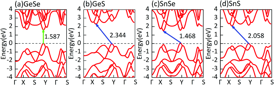 | ||
| Fig. 1 Band structures of monolayer MX in the puckered configuration. Direct and indirect bandgaps are highlighted by green and blue arrows respectively. The bandgap values at the HSE06 level are labeled around the arrows. | ||
Secondly, after the optimization, we turn to construct models of bilayer MX for further study. Through sufficient analysis, we choose four different high-symmetry stacking orders of bilayer MX. These four models are named after AA, AB, AC and AD, respectively, as depicted in Fig. 2. In the AA stacking order, without any change, the upper layer just stacks over the under layer directly. In the AB and AC stacking orders, the upper layer shifts along either the α or β direction by a half lattice constant, respectively. In the AD stacking order, the upper and under layers are the mirror images of each other, shifting one of them along both the α and β directions successively by a half lattice constant to build it. After full optimization, we calculated the relaxed lattice constants and nearest distances between the upper and under layers (dint) of these four structures, listed in Table 2 in order. It is obvious that the changes in lattice constants are mostly small compared with monolayer MX. And dint is larger than that of bulk MX, which can be ascribed to the change in interaction between interlayers. In the same stacking order, the different elementary compositions of MX induce relatively small differences of dint. However, in the same MX material, the differences of dint in the four stacking orders are remarkable.
 | ||
| Fig. 2 (a) The unit cell of bilayer MX. (b–e) Top and side views of the four possible stacking orders (AA, AB, AC, and AD) of bilayer MX. | ||
| AA | AB | AC | AD | |||||||||
|---|---|---|---|---|---|---|---|---|---|---|---|---|
| α (Å) | β (Å) | d int (Å) | α (Å) | β (Å) | d int (Å) | α (Å) | β (Å) | d int (Å) | α (Å) | β (Å) | d int (Å) | |
| GeSe | 3.932 | 4.138 | 3.004 | 3.894 | 4.339 | 3.019 | 3.946 | 4.201 | 3.091 | 3.943 | 4.202 | 3.524 |
| GeS | 3.681 | 4.291 | 3.227 | 3.666 | 4.363 | 2.793 | 3.713 | 4.234 | 2.963 | 3.675 | 4.330 | 3.458 |
| SnSe | 4.226 | 4.254 | 3.227 | 4.211 | 4.348 | 3.016 | 4.252 | 4.236 | 3.060 | 4.241 | 4.250 | 3.626 |
| SnS | 4.051 | 4.132 | 3.187 | 4.029 | 4.132 | 2.906 | 4.078 | 4.079 | 3.025 | 4.064 | 4.113 | 3.599 |
For example, dint ranges from 3.626 to 3.016 Å in the SnSe subsystem. It is clear that the dint is affected strongly by different interactions of stacking orders. In these four stacking orders, the dislocation of the upper and under layers in the AB and AC stacking orders gives more space to accommodate the host atoms. In contrast, the mirror images of each other in the AD stacking order mean the mutual competition of the same atoms having a relatively large incompatibility. Hence, in all structures, the biggest dint of these four MX materials is in AD stacking order without exception. At the same time, the smallest dint is almost in AB stacking order that has the strongest compatibility.
To evaluate the stability of bilayer MX, we calculate the binding energy (Eb), phonon dispersion spectrum, and AIMD to ensure their dynamical stability and thermal stabilities. We obtain the Eb according to the formula which is defined as
| Eb = Ebilayer − 2Emonolayer, | (1) |
| AA | AB | AC | AD | |
|---|---|---|---|---|
| GeSe | −27.534 | −27.935 | −28.473 | −17.081 |
| GeS | −18.867 | −29.385 | −25.508 | −14.705 |
| SnSe | −30.594 | −40.526 | −40.696 | −23.413 |
| SnS | −26.884 | −39.525 | 25.790 | −20.401 |
 | ||
| Fig. 3 (a and b) Side and top views of AC stacking SnS. (c) The charge density of AC stacking SnS. | ||
To check the practical possibility of these structures, we perform phonon dispersion and AIMD simulations. However, a further calculation of their phonon structures indicates that there are only nine structures existing at 0 K. None of them belongs to the GeSe subsystem. The phonon dispersion spectra based on PBE structural parameters are shown in Fig. 4. Furthermore, it is essential to ensure the stability of bilayer MX at finite temperature for their practical application. So the stability of these structures is further investigated by AIMD simulations at finite temperature (300 K) in 3 ps. The results elucidate that bilayer GeS structures are unstable at room temperature, which means that bilayer GeS material may not be synthesized. The AD stacking bilayer SnSe evolves into a new structure that is formed by shifting the upper layer along the α and β directions by a quarter lattice constant successively, as in Fig. 5. After the AIMD simulations, the AD stacking bilayer SnS is also transformed into an unstable structure. Thus, we confirm that five presupposed bilayer MX structures are stable for practical applications.
 | ||
| Fig. 4 Phonon dispersion spectra of stable bilayer MX with PBE optimized lattice parameters at 0 K. | ||
 | ||
| Fig. 5 (a and b) The oblique, top and side views of a new bilayer SnSe structure after the AIMD simulations. | ||
In these five stable structures, for the same MX material, a smaller binding energy tends to be related to a smaller dint illustrated by Tables 2 and 3. The magnitude of binding energy does not show an apparent sequence. Correspondingly, the most stable structure of bilayer MX appears alternately in AB or AC stacking order mainly because of the differences in the electronegativities and atomic radii of anions. The result implies that the staggered structure facilitates the buildup of bilayer MX. Therefore, these two stacking orders are the most reasonable constructions of bilayer MX.
3.2 Electronic structure of bilayer MX
Next, we pay attention to the electronic properties of bilayer MX in detail. The electronic band structures of all stable bilayer MX are shown in Fig. 6. Our calculations demonstrate that these bilayer MX materials are all semiconductors. The contours of their band structures have some change in all stacking orders which can be attributed to the interaction between layers. Fig. 6 indicates the notable decrease of all bandgaps relative to monolayer MX. These variations are consistent with the thickness-dependent bandgap law, which is a general principle for most two-dimensional materials.30,35 As depicted in Fig. 6, the construction of bilayer MX can modulate the bandgap over a wide range. Among them, AB stacking bilayer SnS has the largest bandgap (1.617 eV), while AA stacking bilayer SnSe (0.789 eV) has the smallest bandgap. For the same MX material, the differences between the largest and smallest bandgaps are 0.333 and 0.068 eV respectively. Table 4 lists the percentage relative decreases of bandgaps compared with their monolayer counterpart. We find the maximal decrease of bandgap is up to 46.253%. As a result, the bilayer MX can be used as potential resources for device design. In three cases, the VBM and CBM are located in the same momentum vectors, which is favourable for optical absorption. The direct bandgap is found in AB stacking order SnSe (1.122 eV) and SnS (1.617 eV) and AC stacking order SnSe (0.962 eV). It is well known that the optimal bandgap of a solar cell is about 1.5 eV, which matches well with the direct bandgaps of monolayer GeSe and AB stacking SnS.49 | ||
| Fig. 6 The vertical transitions from the local maxima of the valence band to the local minima of the conduction band are highlighted by green arrows. And the indirect bandgap is indicated by an oblique blue arrow. The values of the bandgaps are labeled around the arrows. The band structures of bilayer SnSe and SnS are aligned in the first and second rows respectively. | ||
| AA (%) | AB (%) | AC (%) | |
|---|---|---|---|
| SnSe | −46.253 | −23.569 | −34.469 |
| SnS | −24.733 | −21.429 | — |
There is another important result that the band structures of bilayer MX possess many conduction-band minima and valence-band maxima. We note that the energy difference between the indirect and direct band gaps is small in several bilayer MX. The values of direct and indirect bandgaps and their absolute differences are given in Table 5. It will be meaningful to accomplish an indirect to direct bandgap transition in these bilayer MX by appropriate external influences.
| AA | AB | AC | |||||||
|---|---|---|---|---|---|---|---|---|---|
| Bandgap | Indirect (eV) | Direct (eV) | Diff (eV) | Indirect (eV) | Direct (eV) | Diff (eV) | Indirect (eV) | Direct (eV) | Diff (eV) |
| SnSe | 0.789 | 0.814 | 0.025 | 1.232 | 1.122 | 0.110 | 1.101 | 0.962 | 0.139 |
| SnS | 1.549 | 1.620 | 0.071 | 1.659 | 1.617 | 0.042 | — | — | — |
In consideration of the flexibility of bilayer MX, like other two-dimensional materials, we achieve indirect-to-direct bandgap transitions by applying a small in-plane uniaxial tensile strain (−3% ≤ ε ≤ 3%) to bilayer MX. For example, 2% or 3% tensile strain along the α direction converts AA and AB stacking bilayer SnS into direct bandgap semiconductors. In the SnSe system, the uniaxial tensile strain is also able to convert indirect into direct bandgaps as illustrated in Fig. 7. From Fig. 7, we find that all direct bandgaps lie in the region between Y and Γ points because of the shift of the CBM.
 | ||
| Fig. 7 Under in-plane uniaxial tensile strain, the direct bandgaps of bilayer MX are all highlighted by green arrows. | ||
These results suggest that the direct bandgap tends to emerge from the configurations possessing approximate lattice constants, i.e. α ≈ β. According to the definition of the structure anisotropy factor κ,
| κ = (α − β)/(α + β) | (2) |
3.3 Response of bilayer MX to an external electric field
As we all know, the properties of two-dimensional materials can be tuned by an external potential field, such as an electric field. Previous theoretical and experimental studies have confirmed that applying a vertical electric field is an effective way to adjust the band structure of two-dimensional materials.50,51 So we focus on the effect of a small external vertical electric field. In view of the limitation of computational resources and the heavy computational cost of the HSE06 method, we determine the electronic properties of bilayer MX just at the PBE level. In bilayer MX, the electronic structure is affected by the potential difference between two MX layers, providing a chance to modulate the bandgap via an external electric field. Meanwhile, when an external electric field is introduced, the band structure will be strongly influenced because of the significant effect of the external electric field on the localized atomic orbitals of bilayer MX. It is interesting to explore the response of bilayer MX to a small external vertical electric field. The responses of different stacking bilayer MX are shown in Fig. 8. We can see that the responses of different stacking bilayer MX are as strong as bilayer phosphorene.36 The external electric field actually provides a way to realize a widely tunable bandgap. The bandgaps of bilayer MX almost decrease linearly with the increase of the vertical electric field, which explicitly indicates the sensitivity of bilayer MX towards the vertical electric field. For bilayer SnSe, when the electric field increases by 0.1 eV Å−1, the bandgap decreases by about 0.3 eV. In bilayer SnS, the rate of bandgap decrease is analogous to that of bilayer SnSe. As depicted in Fig. 8, bilayer MX with wider bandgaps can endure larger electric fields up to 0.35 eV Å−1, but only 0.1 eV Å−1 for the narrow ones. The mechanism behind this phenomenon can be understood as follows. The electronic levels of bilayer MX are split by the external electric field. With the increase of the electronic field, the splitting of conduction bands (CDs) and valence bands (VBs) is enhanced significantly. The initial bandgap is gradually compensated for by the increased split, and even vanishes at some electronic field strength. The widely tunable bandgap under the electric field can be attributed to the giant Stark effect, which has been reported in similar two-dimensional materials, such as black phosphorus, bilayer transition-metal dichalcogenides and boron-phosphide.52–55 In addition, the binary components of bilayer MX can create an internal polar electric field that enhances the potential difference relative to the homogeneous bilayer phosphorene. The interactions in different stacking orders further enhance this effect, which makes bilayer MX more vulnerable to the electric field. According to these results, it can be said that the vertical electric field is able to tune the band structure of bilayer MX over a wide range, which can be utilized in electronic devices. | ||
| Fig. 8 (a) Schematic illustration of the configuration to apply an external vertical electric field to bilayer MX. (b and c) The bandgaps of bilayer MX as a function of the applied external vertical electric field. (a and b) Changes in the bandgaps of bilayer SnSe and SnS under different external vertical electric fields. | ||
4 Conclusions
We have systematically investigated the electronic properties of bilayer MX and the electric-field effect on bilayer MX by performing density functional theory calculations. For each MX material, we construct four stacking models to study the effect of different stacking orders. After careful examination of their dynamical and thermal stabilities, we confirm that five bilayer structures are possible at room temperature. The magnitude of Eb reveals that the force maintaining bilayer MX is beyond pure vdW-like interaction in most situations. The most stable stacking model is found to be of AB or AC stacking order for different MX materials.The electronic structures display a wide bandgap range which is from 0.789 to 1.617 eV for different stacking bilayer MX. The bandgap covers more regions of the visible and infrared spectra. At the same time, an effective approach is proposed to achieve an indirect-to-direct bandgap transition by applying an in-plane uniaxial strain (−3% ≤ ε ≤ 3%). These direct bandgaps are also located over a wide range from 0.902 to 1.624 eV. This result will be beneficial to fabricate high-efficiency modern nano-optoelectronic and photovoltaic devices.
When an external vertical electric field is applied to bilayer MX, the bandgap can be tuned effectively like bilayer phosphorene. The responses of most bilayer MX show poor endurance against the external electric field. Their bandgaps decrease quickly and vanish at some electric field value. This result suggests that both stacking orders and electric field can help in promoting their potential application in nanoelectronics. Combined with the breakthrough in experiment, it is expected that bilayer MX may become promising 2D materials for high-efficiency modern electronic devices in the future.
Conflicts of interest
There are no conflicts to declare.Acknowledgements
This work was supported by the National Natural Science Foundation of China (Grant No. 61366007), the Program of High-End Scientific and Technological Talents in Yunnan Province (Grant No. 2013HA019), and the Program for Excellent Young Talents in Yunnan University. Computational resources were provided by the High Performance Computing Center of Yunnan University.References
- G. Qin, Z. Qin, W. Z. Fang, L. C. Zhang, S. Y. Yue, Q. B. Yan, M. Hu and G. Su, Nanoscale, 2016, 8, 11306–11319 RSC.
- C. Kamal, A. Chakrabarti and M. Ezawa, Phys. Rev. B: Condens. Matter Mater. Phys., 2016, 93, 125428 CrossRef.
- L. C. Gomes, P. E. Trevisanutto, A. Carvalho, A. S. Rodin and A. H. Castro Neto, Phys. Rev. B: Condens. Matter Mater. Phys., 2016, 94, 155428 CrossRef.
- L. C. Gomes, A. Carvalho and A. H. Castro Neto, Phys. Rev. B, 2016, 94, 054103 CrossRef.
- Y. Ding and Y. Wang, Phys. Chem. Chem. Phys., 2016, 18, 23080–23088 RSC.
- G. S. Shi and E. Kioupakis, Nano Lett., 2015, 15, 6926–6931 CrossRef PubMed.
- L. C. Gomes and A. Carvalho, Phys. Rev. B: Condens. Matter Mater. Phys., 2015, 92, 085406 CrossRef.
- A. K. Singh and R. G. Hennig, Appl. Phys. Lett., 2014, 105, 042103 CrossRef.
- A. Shafique and Y. H. Shin, Sci. Rep., 2017, 7, 506 CrossRef PubMed.
- D. J. Xue, S. C. Liu, C. M. Dai, S. Chen, C. He, L. Zhao, J. S. Hu and L. J. Wan, J. Am. Chem. Soc., 2017, 139, 958–965 CrossRef CAS PubMed.
- Y. Zhou, J. Mater. Chem. A, 2016, 4, 10906–10913 CAS.
- P. Ramasamy, D. Kwak, D.-H. Lim, H.-S. Ra and J.-S. Lee, J. Mater. Chem. C, 2016, 4, 479–485 RSC.
- S. Karmakar, C. Chowdhury and A. Datta, J. Phys. Chem. C, 2016, 120, 14522–14530 CAS.
- L. Shi, Y. Li and Y. Dai, ChemPlusChem, 2015, 80, 630–634 CrossRef CAS.
- D. Vaughn, D. Sun, S. M. Levin, A. J. Biacchi, T. S. Mayer and R. E. Schaak, Chem. Mater., 2012, 24, 3643–3649 CrossRef CAS.
- V. L. Deringer, R. P. Stoffel and R. Dronskowski, Phys. Rev. B: Condens. Matter Mater. Phys., 2014, 89, 094303 CrossRef.
- P. C. Kemeny, J. Azoulay, M. Cardona and L. Ley, II, Nuovo Cimento B, 1977, 39, 709–714 CrossRef.
- R. Eymard and A. Otto, Phys. Rev. B: Condens. Matter Mater. Phys., 1977, 16, 1616 CrossRef CAS.
- Y. Hu, S. Zhang, S. Sun, M. Xie, B. Cai and H. Zeng, Appl. Phys. Lett., 2015, 107, 122107 CrossRef.
- J. R. Brent, D. J. Lewis, T. Lorenz, E. A. Lewis, N. Savjani, S. J. Haigh, G. Seifert, B. Derby and P. O'Brien, J. Am. Chem. Soc., 2015, 137, 12689–12696 CrossRef CAS PubMed.
- T. Hu and J. Dong, Phys. Chem. Chem. Phys., 2016, 18, 32514–32520 RSC.
- L. Xu, M. Yang, S. J. Wang and Y. P. Feng, Phys. Rev. B: Condens. Matter Mater. Phys., 2017, 95, 235434 CrossRef.
- T. Hu and J. M. Dong, Phys. Chem. Chem. Phys., 2016, 18, 32514–32520 RSC.
- L. D. Zhao, S. H. Lo, Y. Zhang, H. Sun, G. Tan, C. Uher, C. Wolverton, V. P. Dravid and M. G. Kanatzidis, Nature, 2014, 508, 373–377 CrossRef CAS PubMed.
- R. Fei, W. Li, J. Li and L. Yang, Appl. Phys. Lett., 2015, 107, 173104 CrossRef.
- S. Y. Ma, P. Zhou, L. Z. Sun and K. W. Zhang, Phys. Chem. Chem. Phys., 2016, 18, 8723–8729 RSC.
- C. Kamal and M. Ezawa, Phys. Rev. B: Condens. Matter Mater. Phys., 2015, 91, 085423 CrossRef.
- T. Hu and J. Dong, Phys. Rev. B: Condens. Matter Mater. Phys., 2015, 92, 064114 CrossRef.
- Q. Wei and X. Peng, Appl. Phys. Lett., 2014, 104, 251915 CrossRef.
- H. Liu, A. T. Neal, Z. Zhu, Z. Luo, X. F. Xu, D. Tomanek and P. D. Ye, ACS Nano, 2014, 8, 4033–4041 CrossRef CAS PubMed.
- J. Guan, Z. Zhu and D. Tomanek, Phys. Rev. Lett., 2014, 113, 046804 CrossRef PubMed.
- S. Das, W. Zhang, M. Demarteau, A. Hoffmann, M. Dubey and A. Roelofs, Nano Lett., 2014, 14, 5733–5739 CrossRef CAS PubMed.
- D. Warschauer, J. Appl. Phys., 1963, 34, 1853–1860 CrossRef CAS.
- V. Tran, R. Soklaski, Y. F. Liang and L. Yang, Phys. Rev. B: Condens. Matter Mater. Phys., 2014, 89, 235319 CrossRef.
- J. S. Qiao, X. H. Kong, Z. X. Hu, F. Yang and W. Ji, Nat. Commun., 2014, 5 CAS.
- J. Dai and X. C. Zeng, J. Phys. Chem. Lett., 2014, 5, 1289–1293 CrossRef CAS PubMed.
- L. C. Gomes and A. Carvalho, Phys. Rev. B: Condens. Matter Mater. Phys., 2015, 92 Search PubMed.
- G. Kresse and J. Furthmüller, Phys. Rev. B: Condens. Matter Mater. Phys., 1996, 54, 11169 CrossRef CAS.
- W. Kohn and L. J. Sham, Phys. Rev. B: Condens. Matter Mater. Phys., 1965, 140, A1133–A1138 Search PubMed.
- J. P. Perdew, K. Burke and M. Ernzerhof, Phys. Rev. Lett., 1997, 78, 1396 CrossRef CAS.
- P. E. Blöchl, Phys. Rev. B: Condens. Matter Mater. Phys., 1994, 50, 17953 CrossRef.
- H. J. Monkhorst and J. D. Pack, Phys. Rev. B: Solid State, 1976, 13, 5188 CrossRef.
- J. Heyd, G. E. Scuseria and M. Ernzerhof, J. Chem. Phys., 2003, 118, 8207–8215 CrossRef CAS.
- S. Grimme, J. Comput. Chem., 2006, 27, 1787–1799 CrossRef CAS PubMed.
- L. Huang, F. Wu and J. Li, J. Chem. Phys., 2016, 144, 114708 CrossRef PubMed.
- D. D. Vaughn, R. J. Patel, M. A. Hickner and R. E. Schaak, J. Am. Chem. Soc., 2010, 132, 15170–15172 CrossRef CAS PubMed.
- H. Wiedemeier, H. Georg and V. Schnering Georg, Z. Kristallogr. – Cryst. Mater., 1978, 148, 295 CrossRef CAS.
- T. Bjorkman, A. Gulans, A. V. Krasheninnikov and R. M. Nieminen, Phys. Rev. Lett., 2012, 108, 235502 CrossRef CAS PubMed.
- J. Nelson, The physics of solar cells, Imperial College Press, 2003 Search PubMed.
- Y. B. Zhang, T. T. Tang, C. Girit, Z. Hao, M. C. Martin, A. Zettl, M. F. Crommie, Y. R. Shen and F. Wang, Nature, 2009, 459, 820–823 CrossRef CAS PubMed.
- T. Ohta, A. Bostwick, T. Seyller, K. Horn and E. Rotenberg, Science, 2006, 313, 951–954 CrossRef CAS PubMed.
- X. Chen, C. Tan, Q. Yang, R. Meng, Q. Liang, J. Jiang, X. Sun, D. Q. Yang and T. Ren, Phys. Rev. B: Condens. Matter Mater. Phys., 2016, 18, 16229–16236 CAS.
- Q. Wu, L. Shen, M. Yang, Y. Cai, Z. Huang and Y. P. Feng, Phys. Rev. B: Condens. Matter Mater. Phys., 2015, 92 CAS.
- T. Wang, Y. Liu, Q. Guo, B. Zhang, K. Sheng, C. Li and Y. Yin, J. Korean Phys. Soc., 2015, 66, 1031–1034 CrossRef CAS.
- A. Ramasubramaniam, D. Naveh and E. Towe, Phys. Rev. B: Condens. Matter Mater. Phys., 2011, 84 Search PubMed.
| This journal is © the Owner Societies 2018 |