
Electronic band structures of undoped and P-doped Si nanocrystals embedded in SiO2
E.
Arduca
 *a,
G.
Seguini
a,
C.
Martella
ab,
A.
Lamperti
a,
E.
Napolitani
c,
D.
De Salvador
c,
G.
Nicotra
d,
M.
Scuderi
d,
C.
Spinella
d and
M.
Perego
*a
*a,
G.
Seguini
a,
C.
Martella
ab,
A.
Lamperti
a,
E.
Napolitani
c,
D.
De Salvador
c,
G.
Nicotra
d,
M.
Scuderi
d,
C.
Spinella
d and
M.
Perego
*a
aLaboratorio MDM, IMM-CNR, via C. Olivetti 2, 20864 Agrate Brianza (MB), Italy. E-mail: elisa.arduca@mdm.imm.cnr.it; michele.perego@mdm.imm.cnr.it
bISC-CNR, via dei Taurini 19, I-00185, Roma, Italy
cDipartimento di Fisica e Astronomia, Universita degli Studi di Padova and MATIS IMM-CNR, via Marzolo 8, I-35131 Padova, Italy
dIMM-CNR, Z. I. VIII Strada 5, I-95121 Catania, Italy
First published on 27th November 2017
Abstract
Due to their interesting optical and electronic properties, silicon nanocrystals (Si NCs) are the subject of intense research activity. The definition of their electronic structure is not trivial, neither from a theoretical nor from an experimental point of view. In fact, the models and methodologies developed for bulk materials cannot be directly applied to study these nanostructures where size-related effects, like quantum confinement (QC) and surface related phenomena, play a major role. In this work, X-ray Photoelectron Spectroscopy (XPS) was used to study the electronic structure of Si NCs embedded in SiO2. The energy differences among Si0+ 2s and Si0+ 2p core levels and the valence band maximum (VBM) were monitored. XPS data were combined with a direct measurement of the energy band gap by photoluminescence analysis, providing a complete picture of the electronic structure of Si NCs as a function of their size. Experimental data indicate a progressive reduction of energy differences among core levels and the VBM when decreasing the average diameter of the Si NCs. No concomitant shift of the conduction band minimum (CBM) was observed. The electronic structure of P-doped Si NCs was investigated as well, showing a concurrent shift of the VBM and the CBM as a function of P concentration.
Introduction
Silicon nanocrystals (Si NCs) are particularly appealing for applications in several fields such as microelectronics, optoelectronics, photovoltaics, plasmonics and thermoelectrics.1–4 Their electronic structure is very different compared to the case of bulk silicon due to size-related effects. From a conceptual point of view, Hapala et al.5 demonstrated that the band structure concept is applicable to Si NCs only when their diameter is larger than 2 nm. Below this threshold value, atomic discrete features dominate. As a general principle, Si NCs with at least one dimension smaller than twice the Bohr radius of the exciton in bulk materials exhibit significant modification of their electronic structure, as a consequence of quantum confinement (QC).6–9 Moreover, important competitive effects have to be taken into account, such as the presence of surface induced defects10 and different surface passivation effects.11From an experimental point of view, a clear and complete picture of the electronic structure of Si NCs is still missing. The variation of the band gap, i.e. the relative energy difference between the valence band maximum (VBM) and the conduction band minimum (CBM), was investigated as a function of Si NC size and surface termination. For Si NCs with a diameter smaller than 10 nm, theoretical and experimental work predicts a progressive increase of the band gap as the dimension of Si NCs decreases due to QC.12–15 For Si NCs with fixed diameters, photoluminescence (PL) peaks exhibit a shift toward higher energies changing from the Ar- to the N-terminated surface.16 Several theoretical studies addressed this specific issue and confirmed the influence of interface bonds on the electronic structure of Si NCs.11,17,18 The competition between these two distinct phenomena was systematically addressed.19,20 According to theoretical simulations, for H-terminated Si NCs QC dominates irrespective of their sizes. However, for OH-terminated Si NCs or for Si NCs embedded in a SiO2 matrix, surface effects override QC when their diameter decreases below 2 nm.19
Experimentally, modification of the band gap in very small Si NCs has been widely studied as a function of their size in the case of freestanding Si NCs as well as in the case of Si NCs embedded in a SiO2 matrix.14,21–23 However, very few experimental studies discussed the band alignment of Si NCs in a SiO2 matrix.10,24 Existing data indicated that by reducing the size of Si NCs the variation of the CBM is quite limited, while the shift of the VBM progressively increases. This trend results in a quite symmetrical distribution of the band gap opening for very small Si NCs.
The expected positions of the VBM and the CBM with respect to the vacuum level were calculated in the framework of Density Functional Theory (DFT).11,17,18,25 Interestingly, as a consequence of the different termination of the Si NC surface, theoretical simulations predicted a “drag-down” effect on the VBM of Si NCs, leading to an energetic downshift of the VBM with respect to the vacuum level.11,17,18
More recently, doping of Si NCs was the subject of extensive research activity. As a matter of fact, both n-type (P, As) and p-type (B) impurities were successfully introduced in very small Si NCs by means of different experimental approaches.26–29 However, it is still unclear whether the incorporation of impurities in Si NCs corresponds to effective generation of free charge carriers.30,31 Among all the possible dopants for Si NCs, P represents by far the most common choice in theoretical as well as in experimental work. DFT calculations allowed the investigation of the effect of P incorporation on the Si NCs band structure as a function of different surface termination and different dopant locations.31–33 For P doped Si NCs smaller than 2 nm and covered by OH, interstitial P impurities were predicted to induce deep defect states in the band gap.32 For Si NCs embedded in SiO2, PL experiments were performed to address the modification of the band gap induced by P incorporation. The PL intensity exhibits a clear dependence on the concentration of P incorporated atoms.34–36 In particular, doping with P concentration up to 3 × 1019 cm−3 leads to the enhancement of PL, followed by a progressive PL intensity decrease for higher P concentration.35 At first, on the basis of data reported by Fujii et al.,36 PL enhancement was assumed to be associated with P surface passivation, while the decrease in the PL intensity was attributed to Auger recombination due to P incorporation inside Si NCs.37 Recently, a non-radiative recombination via interstitial P inducing deep defect states in the band gap was proposed as the PL quenching mechanism.33 On the other hand, the energy of the PL emission spectrum exhibits negligible variation as a function of P concentration.34–36 The evolution of the band gap as a function of Si NC size was studied for free-standing Si NCs co-doped with P and B.38 By reducing the size of co-doped Si NCs, the variation of the CBM and of the VBM progressively increases, resulting in a symmetrical distribution of the band gap opening. However, experimental results on the real energy position of the VBM and the CBM after P doping with respect to the energy position in un-doped Si NCs are missing.
In this work, X-ray Photoelectron Spectroscopy (XPS) was used to study the electronic structures of Si NCs embedded in SiO2. The evolution of the electronic structure as a function of Si NC size was characterized for undoped Si NCs, providing information about the alignment of the VBM with respect to Si bulk that was used as reference. XPS data were complemented by PL spectra to obtain a complete picture of the electronic structure of Si NCs with an average dimension ranging from 2.5 to 4.2 nm. The evolution of the electronic structure as a function of the amount of P impurities incorporated in the Si NCs was investigated as well.
Experimental
Si NCs embedded in the SiO2 film were prepared by e-beam evaporation of SiO2 (10 nm)/SiO/SiO2 (10 nm) multilayer structures on Si(100) substrates and subsequent annealing at high temperature in a tubular furnace (1150 °C, 60 min, N2 flux).39 Samples with four different Si NC sizes were prepared varying the thickness of the SiO layer from 2 to 10 nm. During thermal treatment, the SiO film undergoes phase separation, resulting in the nucleation and growth of a 2 dimensional array of Si NCs embedded in the SiO2 matrix.12,30,40 A sample with Si NCs having an average size of 4.2 nm was doped introducing P atoms by means of a solid-state diffusion process. In more detail, the incorporation of P atoms was promoted after the formation of Si NCs by delivering a controlled amount of P atoms from a spatially separated diffusion source.39,41,42 P diffusion sources (P δ-layers) were synthesized by molecular doping (MLD). This methodology allowed the formation of a self-assembled monolayer of dopant-containing molecules on top of the SiO2 film after the formation of NCs. MLD was performed using diethyl 1-propylphosphonate (DPP, Alfa Aesar, purity 97%) as P-containing molecules and mesitylene (Alfa Aesar, purity 98+%) as the solvent.43 The samples were immersed in a solution of mesitylene and DPP (25![[thin space (1/6-em)]](https://www.rsc.org/images/entities/char_2009.gif) :1) and subsequently thermally processed. Annealing was performed at 165 °C for 3 h. After δ-layer formation, samples were capped with 10 nm thick SiO2 films by e-beam evaporation. To promote P diffusion and trapping in Si NCs, the samples were thermally treated in a conventional tubular furnace at 1100 °C for 4 and 8 h.
:1) and subsequently thermally processed. Annealing was performed at 165 °C for 3 h. After δ-layer formation, samples were capped with 10 nm thick SiO2 films by e-beam evaporation. To promote P diffusion and trapping in Si NCs, the samples were thermally treated in a conventional tubular furnace at 1100 °C for 4 and 8 h.
Energy filtered transmission electron microscopy (EFTEM) plan view images of the samples were obtained by using a Cs-probe-corrected JEOL JEM ARM200CF microscope at a primary beam energy of 200 keV operated with the energy image filter-tuned-up at 16 eV corresponding to the Si plasmon oscillation energy and an energy window of 5 eV.
A dual beam ION-TOF IV system was used for Time of Flight Secondary Ion Mass Spectrometry (ToF-SIMS). Sputtering was performed by Cs+ ions at 1 keV and 50 nA, rastering over a 250 × 250 μm2 area. The analysis was carried out in negative polarity by using Ga+ ions operating at 25 keV and 1 pA, rastering over a 50 × 50 μm2 area. Accurate time-to-depth conversion was performed by measuring the average sputter rate in reference Si oxide samples. 31P− signals were calibrated using the protocol reported by M. Mastromatteo et al.41
XPS measurements were performed on a PHI 5600 instrument equipped with a monochromatic Al Kα X-ray source (1486.6 eV) and a concentric hemispherical analyzer with a nominal energy resolution of 0.5 eV. The spectra were collected using a bandpass energy filter at 11.75 eV and a take-off angle of 75°. Polycrystalline Au, Ag, Cu samples were used for energy calibration.
Photoluminescence (PL) measurements were carried out by means of a PL/microRaman system (Renishaw InVia) using the 633 nm line (1.95 eV) of a HeNe laser. The laser radiation was focused on the sample by means of a 100× Leica objective (0.85 numerical aperture), maintaining the incident laser power below 5 mW to avoid sample damage.
Results and discussion
EFTEM analysis of the SiO2/SiO/SiO2 multilayer structures upon high temperature thermal treatment was performed to highlight the formation of Si NCs and to obtain information about their structural characteristics. In Fig. 1 the upper row shows the EFTEM plan view images of the samples having 10 nm (a), 8 nm (b), 6 nm (c), and 4 nm (d) thick deposited SiO layers. The images show the presence of Si NCs in the SiO2 matrix; they can be observed as a bright area over a dark background. NCs are uniformly distributed in the plane they form. In Fig. 1 bottom row, NC size distributions of the samples having 10 nm (e), 8 nm (f), 6 nm (g), and 4 nm (h) thick deposited SiO layers are reported. Data show clear Gaussian like distributions. The average diameters, the standard deviations for the Gaussian like size distributions and the average areal densities determined from the EFTEM plan view are gathered in Table 1. The average size increases from 2.5 to 4.2 nm as the initial SiO layer thickness increases from 2 to 10 nm. The areal density increases as the average dimension of the Si NCs decreases consistently with previous observations reported in the literature.40,44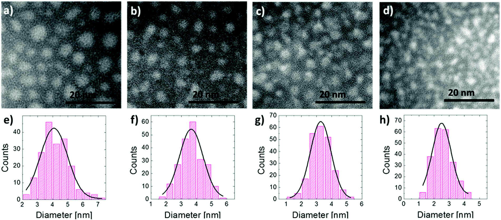 | ||
| Fig. 1 First row, EFTEM plan view images of the samples having 10 nm (a), 8 nm (b), 6 nm (c), and 4 nm (d) thick deposited SiO layers. EFTEM images were acquired upon annealing for 1 h at 1150 °C to induce phase separation and Si NC formation. Second row, NC size distributions of the samples having 10 nm (e), 8 nm (f), 6 nm (g), and 4 nm (h) thick deposited SiO layers. | ||
| Deposited SiO [nm] | Average size [nm] | Density [NCs per nm2] |
|---|---|---|
| 10 | 4.2 ± 0.9 | 0.023 ± 0.002 |
| 8 | 3.6 ± 0.8 | 0.029 ± 0.002 |
| 6 | 3.2 ± 0.7 | 0.038 ± 0.002 |
| 4 | 2.5 ± 0.6 | 0.052 ± 0.002 |
The band structure of Si NCs as a function of their average size was characterized by XPS. Prior to XPS analysis, the thickness of the SiO2 capping layers was reduced to about 2 nm by calibrated HF etching, reducing the distance between the sample surface and the Si NC layer. In this way, photoelectrons directly emitted from the Si NCs could be detected, optimizing the signal to noise ratio in the high-resolution XPS spectra. The full set of the high-resolution spectra of Si 2s, Si 2p core levels and VB regions is reported in Fig. 2.
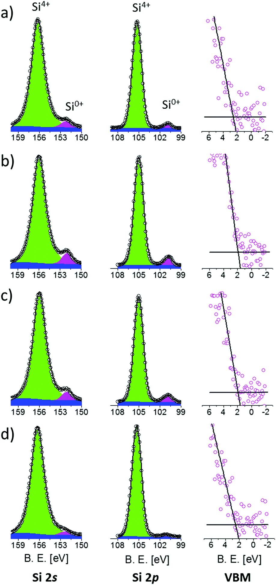 | ||
| Fig. 2 XPS high-resolution spectra of Si 2s, Si 2p and VB regions of the samples having an average Si NC size of 4.2 (a), 3.6 (b), 3.2 (c) and 2.5 nm (d). | ||
Si 2s spectra were fitted with two Voigt functions corresponding to the Si4+ and Si0+ valence states, respectively. A Shirley background function was used to correct the background for the effect of inelastic photoelectron scattering. The Si4+ signals are related to Si atoms in SiO2 while Si0+ signals are related to Si atoms inside a Si matrix. Since the Si NCs layer is spatially separated from the Si substrate by a 10 nm thick SiO2 film, we can exclude contribution to the Si0+ signals associated with photoelectrons emitted from the Si substrate. Therefore, the Si0+ signal entirely originates from Si NCs.45 For all the samples, the position and the FWHM of both signals are in good agreement with data available in the literature.46 The error in peak positioning is estimated to be around 0.05 eV. Actually, Si0+ signals from Si NCs are slightly larger than the ones obtained from crystalline Si bulk. This effect is related to the broadening of the spectra induced by the small size and various orientations of the crystal lattice in Si.42 Moreover, Si4+ signals are shifted with respect to the SiO2 bulk value because of differential charging phenomena occurring during XPS analysis.46
Similarly, after Shirley background subtraction, Si 2p spectra were fitted with a single Voigt function for the Si4+ signal and a doublet of Voigt functions for the Si0+ signal. The doublet of Voigt functions corresponding to Si 2p3/2 and Si 2p5/2 has a spin–orbit splitting of 0.6 eV and a branching ratio of 0.5. For all the samples, the peak position and FWHM are in quite good agreement with data available in the literature.46,49–51 Again, as already observed for the Si 2s spectra, Si0+ peaks from Si NCs result to be slightly larger than those from crystalline Si.47 Interestingly, the energy difference ΔESi 2p–Si 2s between the Si0+ components of the Si 2p and Si 2s core levels is constant within the experimental error. ΔESi 2p–Si 2s is found to be 51.35 ± 0.07 eV irrespective of the Si NC size, indicating that the electronic core levels of Si atoms forming the Si NCs are not significantly affected by QC phenomena. Thus, they can be used as an internal reference to evaluate possible variations in the electronic structure of valence and conduction bands induced by size related effects.
The position of the VBM was determined by the so-called Kraut's methodology, following the standard procedure based on a simple linear extrapolation,52,53 as shown in Fig. 2, right column. Using this approach, the error in VBM positioning is 0.05 eV. The energy difference ΔESi 2p-VBM between the Si0+ components of the Si 2p core levels and the VBM exhibits a progressive reduction with decreasing Si NC size, indicating the evolution of the electronic structure of the valence band due to size-related phenomena. Similar evolution of the energy difference ΔESi 2s-VBM between the Si0+ components of the Si 2s core levels and the VBM is observed.
PL analysis enables to obtain information on the evolution of the band gap of Si NCs as a function of Si NC size. An evident blue shift of PL peaks from 1.1 ± 0.1 to 1.5 ± 0.2 eV is observed with the decrease of the average size of the Si NCs as a consequence of QC.6–9 As noticed by Garrido et al., the emission energy is affected by a Stokes shift of 0.26 ± 0.03 eV with respect to the absorption energy irrespective of the size of Si NCs.54 Thus, the effective band gap value is reported to vary from 1.4 ± 0.1 to 1.8 ± 0.2 eV for the Si NCs with an average diameter corresponding to 4.2 ± 0.9 and 2.5 ± 0.6 nm, respectively. The energy difference ΔESi 2p-CBM between the CBM and the Si0+ component of the Si 2p core level is determined as the sum of ΔESi 2p-VBM obtained by XPS analysis and the band gap value obtained by PL measurements.
In Fig. 3, reconstruction of the Si NC band structure as a function of Si NC size is depicted. Black squares refer to the energy differences ΔESi 2p-VBM/CBM between the Si0+ component of the Si 2p core level and the VBM/CBM in the Si NCs. Data are plotted as a function of Si NC size (left axis). The black dotted lines indicate the ΔESi 2p-VBM/CBM reference values for crystalline Si bulk, ΔESi 2p-CBM was obtained by adding the tabulated Si band gap energy55 to the measured ΔESi 2p-VBM value. On the right axis, the ΔESi 2p-VBM/CBM values are rescaled using the VBM of crystalline Si bulk as a reference for the energy scale. For the Si NCs with an average size of 4.2 nm, the ΔESi 2p-VBM value is equal to the value in bulk crystalline Si, while ΔESi 2p-CBM shifts towards higher energy. A gradual decrease of the ΔESi 2p-VBM values as a function of Si NC size is measured, pointing out the progressive influence of QC effects on the VBM.6–9 The corresponding ΔESi 2p-CBM value remains roughly constant within the experimental error, irrespective of Si NC size. This corresponds to an average CBM shift of 0.58 ± 0.09 eV with respect to the CBM in bulk Si. The solid black line corresponds to the average position of the CBM in the Si NCs. It is worth comparing our results with those reported in the literature for similar systems. For Si NCs embedded in SiO2 and synthesized by ion implantation, Barbagiovanni et al.48 claimed that ΔESi 2p-VBM does not change as a function of Si NC size. However Barbagiovanni et al.48 did not directly measure the dimension of Si NCs. They simply calculated the average diameter of Si NCs from the PL peak position comparing various theoretical models. As clearly highlighted in their original manuscript, each model gives a very different Si NC average size for a single set of experimental data. For example, the calculated average Si NC diameter for the sample with the smallest Si NCs varies from 1.55 nm up to 8 nm, depending on the specific theoretical model used to determine the size. This uncertainty in determining the Si NC size makes quite difficult the comparison with data reported by Barbagiovanni et al.48 For Si NCs synthesized by thermal vaporization of Si in an Ar buffer, Van Buuren et al.56 measured a variation of ΔESi 2p-VBM as a function of Si NC size. Their results are in perfect agreement with data presented in Fig. 3. On the other hand, they measured a small CBM variation of 0.1–0.2 eV with respect to the CBM of Si bulk, which is significantly lower than 0.58 ± 0.09 eV measured here. Similarly, the values of ΔESi 2p-VBM as a function of Si NC size that we obtained are perfectly consistent with data reported by Hori et al.18 for B and P co-doped colloidal Si NCs with an average diameter ranging from 2 to 4.5 nm. The variation of the CB offset in these co-doped Si NCs is around 0.1–0.2 eV in agreement with the data reported by Van Buuren et al. It is worth noting that in our case, the position of the CBM was determined combining XPS data to determine ΔESi 2p-VBM and PL measurements to obtain information on band gap evolution as a function of Si NC size. PL emission energies were corrected by a Stokes shift of 0.26 ± 0.03 eV with respect to the absorption energy irrespective of the size of the Si NCs.54 If we neglect this correction the shift of the CBM that we measured is perfectly consistent with those reported by Van Buuren et al. and by Hori et al. in their manuscripts. This discrepancy with respect to our experimental results could be ruled out considering that in this work we focused on Si NCs embedded in the SiO2 matrix, while the manuscripts by Van Buuren et al. and by Hori et al. focused on H-terminated freestanding Si NCs. As was previously demonstrated, the Si NC surface plays an important role in determining the electronic structure of Si NCs.11,16–18,25 Thus, the difference in surface termination could be responsible for the variation in CBM evolution.
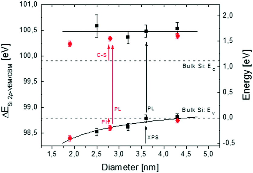 | ||
| Fig. 3 Reconstruction of the Si NC band structure as a function of Si NC size. Black squares refer to the energy difference ΔESi 2p-VBM/CBM as a function of Si NC size (left axis). Error bars refer to the experimental error of XPS and PL analyses. The black dotted lines indicate the reference band structure for a crystalline Si bulk. Red points refer to Seguini et al. (right axis)10 where independent measurements of the CBM and VBM energy positions with respect to the SiO2 matrix were acquired by means of PI and C-S, respectively. | ||
In previous work, Seguini et al.10 measured the evolution of the band structure as a function of Si NC size for Si NCs embedded in SiO2 by means of electro-optical characterization techniques. Independent measurements of the CBM and VBM energy positions with respect to the SiO2 matrix were acquired by means of photo-ionization (PI) and capacitance spectroscopy (C-S), respectively. Data obtained by Seguini et al. are plotted in Fig. 3 (red points, right axis). These data are in very good agreement with those of the present work. By decreasing the size of Si NCs, three different regimes were identified; at first, QC affects the CB that shifts to high energy values, then surface effects pin the conduction states, and finally QC modifies the VB with a shift towards low energy values.10 The first two effects are clearly confirmed by our experiments, while the third cannot be addressed because it is out of our Si NC size range. The overall picture obtained by the comparison between our experimental findings and literature data suggests that the position of the VBM is merely determined by QC effects while the CBM position is significantly affected by surface states determining a significant variation of the CBM shift.
The effect of the incorporation of P impurity atoms in Si NCs with an average size of 4.2 nm was then investigated in detail. P was introduced in Si NCs by delivering a controlled amount of dopant atoms from a spatially separated diffusion source.39,41,42 The diffusion source was synthesized by MLD on top of the SiO2 matrix and then capped with a 10 nm layer of SiO2.43 In order to promote P diffusion and its trapping in Si NCs without perturbing the equilibrium structure of the Si NCs, thermal treatments for P diffusion were performed at 1100 °C. This temperature is significantly lower than the one used for the synthesis of Si NCs. The effective stability of Si NCs during high temperature thermal treatments for P diffusion and incorporation has already been demonstrated.39 For this experiment different annealing times corresponding to 4 and 8 h were considered, reaching two different doping concentration levels in Si NCs.
Fig. 4(a) shows a representative ToF-SIMS depth profile of the sample upon annealing for 4 h at 1100 °C. The secondary ion signals were normalized on the average value of the 30Si− signal in the SiO2 substrate, to remove variations of the signal intensity due to fluctuations of the Ga+ current. 28Si2− and 28SiO3− normalized profiles are reported to describe the sample structure (left axis). The 28SiO3− signal is indicative of the oxide matrix. The 28Si2− signal shows a peak at a depth of 30 nm that is used as a marker of the presence of an excess of silicon associated with the Si NCs within the SiO2 matrix.57,58 ToF-SIMS data confirm that the Si NC plane is embedded in the SiO2 matrix and is spatially separated from the Si substrate by a 10 nm thick SiO2 layer. The FWHM of the 28Si2− peak is correlated with the average size of Si NCs and results to be 3.3 ± 0.2 nm.58 The stability of the Si NC structure during the doping process was further checked monitoring the FWHM of the 28Si2− peak. FWHM values are constant, within the experimental error, irrespective of thermal treatment. The calibrated P depth profile is reported as well (violet line, right axis). P signal calibration was performed following a previously defined protocol.41 ToF-SIMS data show that, upon thermal treatment, P atoms diffuse in the SiO2 and accumulate in the Si NC region. No P accumulation in the SiO2 layer between the Si NCs and the Si substrate is observed. The same behaviour was observed for the sample annealed at 1100 °C for 8 h. Different P concentration levels were observed in the Si NCs.
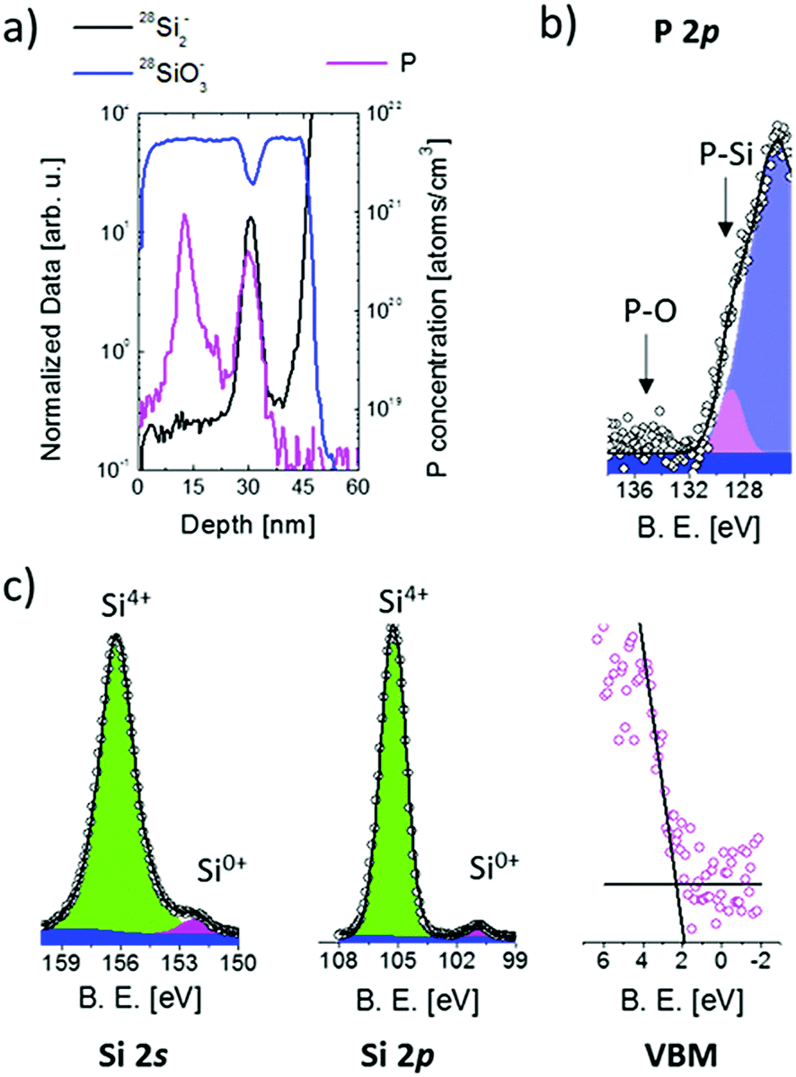 | ||
| Fig. 4 (a) ToF-SIMS calibrated P depth profile of the sample having average Si NC size of 4.2 nm upon annealing for 4 h at 1100 °C (violet line, right axis). 28Si2− and 28SiO3− normalized depth profiles are reported either (black and blue lines, left axis); XPS high-resolution spectra of the P 2p region (b) and of Si 2s, Si 2p and VB regions (c) for the same sample. | ||
In Fig. 4(b) the XPS high-resolution spectrum of the P 2p core level is reported for the same sample with Si NCs having an average size of 4.2 nm. The spectrum was acquired upon thermal treatment at 1100 °C for 4 h. The thickness of the SiO2 capping layer was reduced to 2 nm by calibrated HF etching before XPS analysis. The fitting of the experimental data was performed considering a simple Voigt function to fit the P 2p spectral line (pink peak) and a Gaussian curve for the loss structure (violet peak) of the intense Si 2p signal located at 100 eV following the procedure reported elsewhere.29,39 The FWHM of the Gaussian curve was fixed equal to the Gaussian curve's FWHM experimentally determined for the sample without P (data not shown). The P 2p signal is centered at ∼129 eV corresponding to P atoms in a Si matrix.59 On the basis of XPS data, we can safely assume that all P atoms are trapped inside Si NCs consistently with our previous findings on similar systems.39 Starting from this assumption it is possible to determine from ToF-SIMS P depth profiles the effective concentration of P atoms in Si NCs (cNCsP). cNCsP reached values as high as 1.9%.
XPS high-resolution spectra of Si 2s, Si 2p and the VB region for the sample annealed at 1100 °C for 4 h are reported in Fig. 4(c). The spectra were analysed following the procedure described in the previous paragraphs to determine the energy differences ΔESi 2p-VBM and ΔESi 2s-VBM. The energy difference ΔESi 2p–Si 2s between the Si0+ components of the Si 2p and Si 2s core levels is constant irrespective of cNCsP. A progressive decrease of ΔESi 2p-VBM and ΔESi 2s-VBM is observed upon increasing P concentration in the Si NCs. PL analysis was performed on the sample with the higher P concentration. No difference in the PL peak position before and after doping was found, as reported in the literature for doped Si NCs embedded in a SiO2 matrix.34–36
In Fig. 5, reconstruction of the Si NC band structure as a function of cNCsP is depicted combining XPS and PL data. The black dotted lines indicate the reference band structure for a crystalline bulk Si.
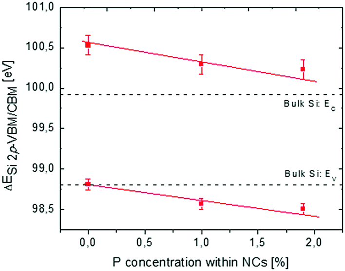 | ||
| Fig. 5 Reconstruction of the electronic band structure for Si NCs having an average size of 4.2 nm as a function of cNCsP. Red squares refer to the difference ΔESi 2p-VBM/CBM. Error bars refer to experimental errors of XPS and PL analyses. The black dotted lines indicate the reference band structure for a crystalline Si bulk. | ||
Collected data indicate a significant decrease of the energy difference ΔESi 2p-VBM/CBM as the cNCsP increase. This effect is unexpected and cannot be simply explained as a direct consequence of P-doping of the Si NCs. In bulk semiconductors doping would correspond to a rigid shift of the electronic band structure and core levels determined by the different Fermi level of the system. The shift of the VBM and the CBM with respect to the Si 2p core level suggests a different scenario.
This shift of the VBM and the CBM as a function of cNCsP could be related to the higher electronegativity (EN) and ionization energy (Eion) of P with respect to Si. The higher the EN, the higher the ionicity of the bond between P and Si, suggesting preferential localization of the bonding-electrons on P atoms. Collected data suggest that the Eion value of P could locally govern the energetic structure of Si NCs. In our systems, P atoms could influence the entire energetic structure of Si NCs, as the cNCsP are very high considering that the solid solubility of P in Si is about 1%.60 As a result, a “drag-down” effect on the NC energy levels with lower binding energies is observed. Conversely, the electrons of Si atomic core levels are not affected by the doping, probably because of their proximity with the atomic core levels and their weak interaction with the P impurities introduced in the Si NCs. In the framework of DFT, a similar “drag-down” effect was predicted for Si NCs terminated with X elements more electronegative than Si and with a Eion higher than that of Si.11,17,18,25 It is worth saying that the comparison between those theoretical results and collected data is not trivial. First, the simulated Si NCs are smaller than the one synthesized for this work. Second, in the DFT framework Si NCs are fully covered by X elements, while data presented here refer to the Si NCs containing P in the interior. Moreover, for simulated Si NCs, the percentage concentration of X atoms in Si NC (cNCsX) is more than five times higher than the measured cNCsP.
On the other hand, it is worth noting that the possibility to reach high cNCsP values has already been investigated by several authors, showing the capability to reach impurity levels even higher than 10%.33,61–63 Such high concentrations of P are well above P solubility in the bulk silicon and are commonly explained assuming the formation of the Si–P alloy.33,61 Interestingly, DFT calculations predicted significant modification of the band structure of a crystalline Si3P4 alloy, with respect to the crystal Si case.64 In principle, the observed variation of the band structure in P-doped Si NCs could be related to the modification of the VB and CB localized state induced by Si–P alloying. Actually, these high levels of impurities are not relevant for electronic doping, as most impurities are electrically inactive, though there is broad interest in the peculiar plasmonic properties of these nanostructures.61,63
The real nature of the shifts of the VBM and the CBM with respect to the Si 2p core level is not clear yet and the present data do not allow discriminating among the different hypotheses. Further work is necessary to elucidate this point and provide proper interpretation of the experimental data reported herein.
Conclusions
The evolution of the electronic structure as a function of Si NCs size was characterized in undoped Si NCs with an average size ranging from 2.5 to 4.2 nm. In particular, we observed that the electronic structure of core levels is not affected by QC effects. On the other hand, clear variations of the VBM are recorded as a function of Si NC size. The evolution of the electronic structure as a function of cNCsP was investigated for P-doped Si NCs having an average size of 4.2 nm. Upon increasing cNCsP, the VBM and the CBM shift towards higher binding energy indicating that P impurity atoms play an important role in the definition of the electronic band structure of Si NCs.Conflicts of interest
There are no conflicts of interest to declare.Acknowledgements
The authors would like to acknowledge Stefano Danesi (Universita degli Studi di Padova), for his help on the synthesis of P δ-layers by MLD, and Mario Alia (Laboratorio MDM, IMM-CNR) for technical support. This research has been partially supported by the Italian MIUR project Beyond-Nano (PON a3_00363).References
- M. C. Beard, K. P. Knutsen, P. Yu, J. M. Luther, Q. Song, W. K. Metzger, R. J. Ellingson and A. J. Nozik, Nano Lett., 2007, 7, 2506–2512 CrossRef CAS PubMed.
- J. Tang, H. T. Wang, D. H. Lee, M. Fardy, Z. Huo, T. P. Russell and P. Yang, Nano Lett., 2010, 10, 4279–4283 CrossRef CAS PubMed.
- F. Priolo, T. Gregorkiewicz, M. Galli and T. F. Krauss, Nat. Nanotechnol., 2014, 9, 19–32 CrossRef CAS PubMed.
- R. Gresback, N. J. Kramer, Y. Ding, T. Chen, U. R. Kortshagen and T. Nozaki, ACS Nano, 2014, 8, 5650–5656 CrossRef CAS PubMed.
- P. Hapala, K. Kusova, I. Pelant and P. Jelinek, Phys. Rev. B: Condens. Matter Mater. Phys., 2013, 87, 1954 CrossRef.
- Q. Xu, J. W. Luo, S. S. Li, J. B. Xia, J. Li and S. H. Wei, Phys. Rev. B: Condens. Matter Mater. Phys., 2007, 75, 235304 CrossRef.
- M. G. Mavros, D. a. Micha and D. S. Kilin, J. Phys. Chem. C, 2011, 115, 19529–19537 CAS.
- A. M. Hartel, D. Hiller, S. Gutsch, P. Löper, S. Estradé, F. Peiró, B. Garrido and M. Zacharias, Thin Solid Films, 2011, 520, 121–125 CrossRef CAS.
- J. H. Warner, A. Hoshino, K. Yamamoto and R. D. Tilley, Angew. Chem., Int. Ed., 2005, 44, 4550–4554 CrossRef CAS PubMed.
- G. Seguini, C. Castro, S. Schamm-Chardon, G. Benassayag, P. Pellegrino and M. Perego, Appl. Phys. Lett., 2013, 103, 23103 CrossRef.
- D. König, J. Rudd, M. A. Green and G. Conibeer, Phys. Rev. B: Condens. Matter Mater. Phys., 2008, 78, 35339 CrossRef.
- L. Mangolini, J. Vac. Sci. Technol., B: Microelectron. Nanometer Struct.–Process., Meas., Phenom., 2013, 31, 20801 Search PubMed.
- T. Shimizu-Iwayama, N. Kurumado, D. E. Hole and P. D. Townsend, J. Appl. Phys., 1998, 83, 6018–6022 CrossRef CAS.
- M. Zacharias, J. Heitmann, R. Scholz, U. Kahler, M. Schmidt and J. Blasing, Appl. Phys. Lett., 2002, 80, 661–663 CrossRef CAS.
- S. Furukawa and T. Miyasato, Phys. Rev. B: Condens. Matter Mater. Phys., 1988, 38, 5726–5729 CrossRef CAS.
- D. König, D. Hiller, S. Gutsch and M. Zacharias, Adv. Mater. Interfaces, 2014, 1, 1400359 CrossRef.
- F. A. Reboredo and G. Galli, J. Phys. Chem. B, 2005, 109, 1072–1078 CrossRef CAS PubMed.
- A. Carvalho, S. Öberg, M. J. Rayson and P. R. Briddon, Phys. Rev. B: Condens. Matter Mater. Phys., 2012, 86, 45308 CrossRef.
- R. Guerra, E. Degoli and S. Ossicini, Phys. Rev. B: Condens. Matter Mater. Phys., 2009, 80, 155332 CrossRef.
- M. Bürkle, M. Lozac’h, C. Mcdonald, D. Mariotti, K. Matsubara and V. Švrček, Adv. Funct. Mater., 2017, 1701898, 1–7 Search PubMed.
- T. Nozaki, K. Sasaki, T. Ogino, D. Asahi and K. Okazaki, Nanotechnology, 2007, 18, 235603 CrossRef.
- J. Choi, N. S. Wang and V. Reipa, Langmuir, 2007, 23, 3388–3394 CrossRef CAS PubMed.
- B. Garrido Fernandez, M. López, C. García, A. Pérez-Rodríguez, J. R. Morante, C. Bonafos, M. Carrada and A. Claverie, J. Appl. Phys., 2002, 91, 798–807 CrossRef CAS.
- G. Seguini, S. Schamm-Chardon, P. Pellegrino and M. Perego, Appl. Phys. Lett., 2011, 99, 82107 CrossRef.
- A. Gali, M. Vörös, D. Rocca, G. T. Zimanyi and G. Galli, Nano Lett., 2009, 9, 3780–3785 CrossRef CAS PubMed.
- F. Ruffino, L. Romano, E. Carria, M. Miritello, M. G. Grimaldi, V. Privitera and F. Marabelli, J. Nanotechnol., 2012, 2012, 1–6 CrossRef.
- M. Fujii, S. Hayashi and K. Yamamoto, J. Appl. Phys., 1998, 83, 7953–7957 CrossRef CAS.
- H. Gnaser, S. Gutsch, M. Wahl, R. Schiller, M. Kopnarski, D. Hiller and M. Zacharias, J. Appl. Phys., 2014, 115, 34304 CrossRef.
- M. Perego, C. Bonafos and M. Fanciulli, Nanotechnology, 2010, 21, 25602 CrossRef PubMed.
- S. Gutsch, J. Laube, D. Hiller, W. Bock, M. Wahl, M. Kopnarski, H. Gnaser, B. Puthen-Veettil and M. Zacharias, Appl. Phys. Lett., 2015, 106, 113103 CrossRef.
- D. König, S. Gutsch, H. Gnaser, M. Wahl, M. Kopnarski, J. Göttlicher, R. Steininger, M. Zacharias and D. Hiller, Sci. Rep., 2015, 5, 9702 CrossRef PubMed.
- Z. Ni, X. Pi and D. Yang, Phys. Rev. B: Condens. Matter Mater. Phys., 2014, 89, 35312 CrossRef.
- D. Hiller, J. López-Vidrier, S. Gutsch, M. Zacharias, K. Nomoto and D. König, Sci. Rep., 2017, 7, 863 CrossRef PubMed.
- G. A. Kachurin, S. G. Yanovskaya, D. I. Tetelbaum and A. N. Mikhailov, Semiconductors, 2003, 37, 713 CrossRef CAS.
- A. L. Tchebotareva, M. J. A. De Dood, J. S. Biteen, H. A. Atwater and A. Polman, J. Lumin., 2005, 114, 137–144 CrossRef CAS.
- M. Fujii, A. Mimura, S. Hayashi and K. Yamamoto, Appl. Phys. Lett., 1999, 75, 184 CrossRef CAS.
- A. Mimura, D. Kovalev and F. Koch, Phys. Rev. B: Condens. Matter Mater. Phys., 2000, 62, 625–627 CrossRef.
- Y. Hori, S. Kano, H. Sugimoto, K. Imakita and M. Fujii, Nano Lett., 2016, 16, 2615–2620 CrossRef CAS PubMed.
- M. Perego, G. Seguini, E. Arduca, J. Frascaroli, D. De Salvador, M. Mastromatteo, A. Carnera, G. Nicotra, M. Scuderi, C. Spinella, G. Impellizzeri, C. Lenardi and E. Napolitani, Nanoscale, 2015, 7, 14469–14475 RSC.
- J. Heitmann, F. Müller, M. Zacharias and U. Gösele, Adv. Mater., 2005, 17, 795–803 CrossRef CAS.
- M. Mastromatteo, E. Arduca, E. Napolitani, G. Nicotra, D. De Salvador, L. Bacci, J. Frascaroli, G. Seguini, M. Scuderi, G. Impellizzeri, C. Spinella, M. Perego and A. Carnera, Surf. Interface Anal., 2014, 46, 393–396 CrossRef CAS.
- M. Mastromatteo, E. Arduca, E. Napolitani, G. Nicotra, D. De Salvador, L. Bacci, J. Frascaroli, G. Seguini, M. Scuderi, G. Impellizzeri, C. Spinella, M. Perego and A. Carnera, J. Mater. Chem. C, 2016, 4, 3531 RSC.
- E. Arduca, M. Mastromatteo, D. De Salvador, G. Seguini, C. Lenardi and E. Napolitani, Nanotechnology, 2016, 27, 75606 CrossRef PubMed.
- B. Han, Y. Shimizu, G. Seguini, E. Arduca, C. Castro, G. Ben Assayag, K. Inoue, Y. Nagai, S. Schamm-Chardon and M. Perego, RSC Adv., 2016, 6, 3617–3622 RSC.
- S. Kim, M. C. Kim, S. H. Choi, K. J. Kim, H. N. Hwang and C. C. Hwang, Appl. Phys. Lett., 2007, 91, 14–17 Search PubMed.
- S. Iwata and A. Ishizaka, J. Appl. Phys., 1996, 79, 6653–6713 CrossRef CAS.
- D. Briggs and M. P. Seah, Pratical Surface Analysis. Volume 1: Auger and X-ray Photoelectron Spectroscopy, 1990 Search PubMed.
- E. Barbagiovanni, L. Goncharova and P. Simpson, Phys. Rev. B: Condens. Matter Mater. Phys., 2011, 83, 35112 CrossRef.
- A. Dane, U. K. Demirok, A. Aydinli and S. Suzer, J. Phys. Chem. B, 2006, 110, 1137–1140 CrossRef CAS PubMed.
- K. S. Min, K. V. Shcheglov, C. M. Yang, H. A. Atwater, M. L. Brongersma and A. Polman, Appl. Phys. Lett., 1996, 69, 2033–2035 CrossRef CAS.
- T. P. Chen, Y. Liu, C. Q. Sun, M. S. Tse, J. H. Hsieh, Y. Q. Fu, Y. C. Liu and S. Fung, J. Phys. Chem. B, 2004, 108, 16609–16612 CrossRef CAS.
- E. A. Kraut, R. W. Grant, J. R. Waldrop and S. P. Kowalczyk, Phys. Rev. B: Condens. Matter Mater. Phys., 1983, 28, 1965–1977 CrossRef CAS.
- M. Perego and G. Seguini, J. Appl. Phys., 2011, 110, 53711 CrossRef.
- B. Garrido, M. López, O. González, A. Pérez-Rodríguez, J. R. Morante and C. Bonafos, Appl. Phys. Lett., 2000, 77, 3143 CrossRef CAS.
- D. Kovalev, H. Heckler, M. Ben-Chorin, G. Polisski, M. Schwartzkopff and F. Koch, Phys. Rev. Lett., 1998, 81, 2803–2806 CrossRef CAS.
- T. van Buuren, L. Dinh, L. Chase, W. Siekhaus and L. Terminello, Phys. Rev. Lett., 1998, 80, 3803–3806 CrossRef CAS.
- M. Perego, S. Ferrari, S. Spiga, E. Bonera, M. Fanciulli and V. Soncini, Appl. Phys. Lett., 2003, 82, 121–123 CrossRef CAS.
- M. Perego, S. Ferrari, M. Fanciulli, G. Ben Assayag, C. Bonafos, M. Carrada and A. Claverie, Appl. Surf. Sci., 2004, 231–232, 813–816 CrossRef CAS.
- A. I. Kovalev, D. L. Wainstein, D. I. Tetelbaum, W. Hornig and Y. N. Kucherehko, Surf. Interface Anal., 2004, 36, 959–962 CrossRef CAS.
- P. Pichler, Intrinsic Point Defects, Impurities, and Their Diffusion in Silicon, Springer, Wien, 2004, ch. 5 Search PubMed.
- S. Zhou, X. Pi, Z. Ni, Y. Ding, Y. Jiang, C. Jin and C. Delerue, ACS Nano, 2015, 9, 378–386 CrossRef CAS PubMed.
- R. Khelifi, D. Mathiot, R. Gupta, D. Muller, M. Roussel and S. Duguay, Appl. Phys. Lett., 2013, 102, 13116 CrossRef.
- D. J. Rowe, J. S. Jeong, K. A. Mkhoyan and U. R. Kortshagen, Nano Lett., 2013, 13, 1317 CrossRef CAS PubMed.
- M. Huang, Y. P. Feng, A. T. L. Lim and J. C. Zheng, Phys. Rev. B: Condens. Matter Mater. Phys., 2004, 69, 54112 CrossRef.
| This journal is © The Royal Society of Chemistry 2018 |