
Solution-processed N-trialkylated triindoles for organic field effect transistors†
C.
Ruiz
a,
I.
Arrechea-Marcos
b,
A.
Benito-Hernández
a,
E.
Gutierrez-Puebla
 a,
M. A.
Monge
a,
J. T.
López Navarrete
b,
M. C.
Ruiz Delgado
b,
R. Ponce
Ortiz
b and
Berta
Gómez-Lor
*a
a,
M. A.
Monge
a,
J. T.
López Navarrete
b,
M. C.
Ruiz Delgado
b,
R. Ponce
Ortiz
b and
Berta
Gómez-Lor
*a
aMaterials Science Factory, Instituto de Ciencia de Materiales de Madrid, CSIC, C/Sor Juana Inés de la Cruz 3, Cantoblanco, Madrid 28049, Spain. E-mail: bgl@icmm.csic.es
bDepartamento de Química Física, Facultad de Ciencias, Universidad de Málaga, Campus de Teatinos, 29071, Málaga, Spain
First published on 28th November 2017
Abstract
Three crystalline N-trialkyltriindoles in which the length of the alkyl chains attached to the nitrogen has been enlarged from a methyl to a butyl and to a hexyl group have been investigated in the search for semiconducting triindole easy to process from solution. We have found that the number of carbon atoms of the N-alkyl chains has a significant impact on how these molecules interact with each other in the bulk materials and it strongly influences the final morphology of the crystals, which grow as long crystalline wires, cubes or microbelts. Single crystal analysis allows us to recognize the contribution of several cooperative CH–π interactions to guide the self-assembly of these types of molecules. In addition, alkyl chain engineering allows triindole derivatives processable for solution, which render OFETs showing field effect mobilities of 0.03 cm2 V−1 s−1 and 6 × 10⁻³ cm2 V−1 s−1 when vapor deposited and drop casted, respectively. The results of this study represent a step forward towards the rational control of the supramolecular arrangement of this high performance semiconducting platform, this being a key fact for designing efficient solution-processed organic semiconductors.
Introduction
The use of molecular semiconductors for low-cost, flexible and large-area electronic devices1,2 has expanded impressively in the last few years. The great expectations devoted to organic materials lately rely on their electronic and mechanical properties and the possibility of fine-tuning their key properties through a convenient molecular design. Extended aromatic systems are desirable because they provide a number of “mobile” π-electrons and their electronic properties can be readily modulated by the introduction of functional groups into defined positions of the molecules.3 However, the fundamental properties of molecular materials are governed not only by those of individual molecules but also by their spatial ordering in the bulk.Electronic devices involve charge transport as their main operation process and charge transport is highly dependent on electronic coupling between neighbouring units, which in turn depend on the intermolecular order.4–7 In fact, highest mobilities have been determined in perfectly ordered crystalline materials. Unfortunately, organic single crystals are fragile and difficult to process, and their incorporation into devices often requires manual selection and handling of individual crystals. Alternatively, crystalline semiconductors have been incorporated into devices as films prepared by vaporization and condensation onto the desired substrate. However, the need of an evaporation step eliminates the easy-to-process advantages of organic electronics. At this stage, solution processability is an indispensable requirement for large area low cost mass production.
There is therefore, much interest in functional molecules able to self-organize through the action of intermolecular interactions, providing bulk ordered materials upon solution evaporation, which requires a deep knowledge of the non-covalent interactions existing among the molecules. This is usually a challenging task as intermolecular interactions involving π-conjugated systems are weak in nature and act in a cooperative way but often in opposite directions complicating their understanding.8–11 Single crystal analysis provides invaluable information on the nature of intermolecular interactions among neighbouring units and offers an excellent opportunity to investigate the molecular arrangement dependent properties.
In this context we became interested in the electron-rich 10,15-dihydro-5H-diindolo[3,2-a:3′,2′-c]carbazole (triindole) as a self-assembling p-type organic semiconductor. This molecule has been shown to have a strong tendency to self-assemble into one-dimensional superstructures both in solution12 and in the bulk.13 Triindole-based single crystalline or liquid crystalline materials have been found to exhibit very high hole mobilities since they combine the good intrinsic charge transport properties with a high tendency to organize in stacked supramolecular arrangements providing a path for charge carriers. In fact, triindole-based liquid crystals present hole mobilities above 2 cm2 V−1 s−1 qualifying triindoles among the highest hole mobility semiconducting mesogens.14 Crystalline triindoles have shown mobility values of up to 0.4 cm2 V−1 s−1 as determined by SCLC on single crystals of N-trimethyltriindole13 and up to 3 × 10⁻² cm2 V−1 s−1 when this compound was incorporated as a sublimed thin film in a field effect transistor.15 However, efficient triindole-based transistors processed from solution are still lacking.16,17
We approach here the study of a family of triindole semiconductors functionalized with different lengths of N-alkyl chains in order to shed light on the effect that these chains exert on the organization preferences and electronic properties of N-alkyl triindoles towards the development of solution processed OFETs. Attaching alkyl chains to improve solution-processability of semiconducting molecules is a common design strategy, however the effect of the alkyl chains in their self-assembly is not always evident.5 The investigation of the crystal structures of different N-trialkylated single crystalline triindoles demonstrates that the size of the alkyl chains has an important effect on their tendency to self-assemble, and points towards cooperative CH–π interactions in the origin of the different superstructures observed. The influence of the diverse alkyl chains on the electrical performance and processability of these materials have been evaluated by incorporating them into OFET devices both by evaporation and solution processes. DFT calculations help us to rationalize the role played by the N-alkyl chains in the electronic properties by analysing the changes in the main molecular charge-transport parameters as a function of the length of the alkyl chain (Fig. 1).
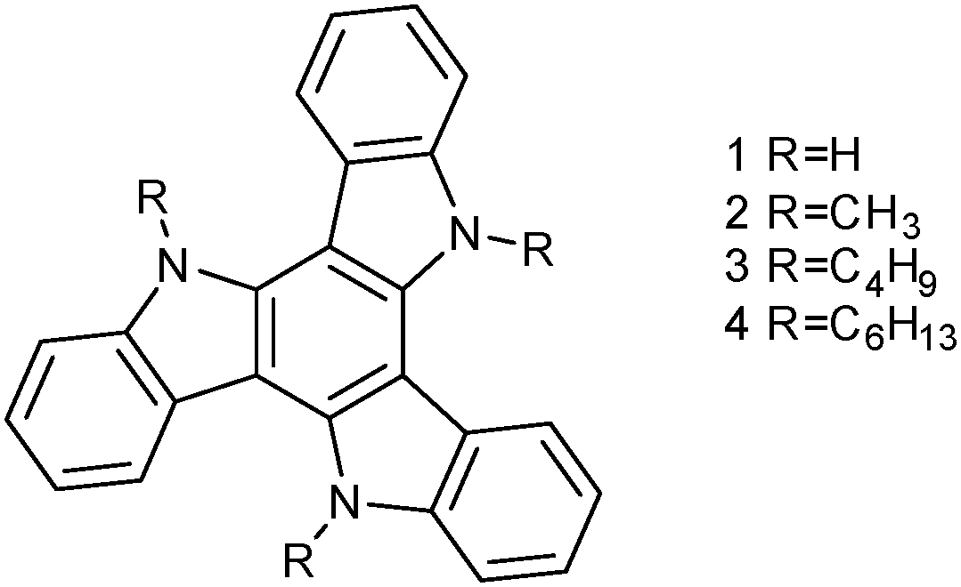 | ||
| Fig. 1 Chemical structure of N-trialkylsubstituted triindoles 1–4. | ||
Results and discussion
Synthesis and electronic properties
Compounds 2–4 can be readily obtained by alkylation of triindole 1 in the presence of a phase transfer catalyst as previously reported.13,18,19 The length of the alkyl chains does not affect significantly their electronic properties. In solution the UV-vis spectra and cyclic voltammograms of 2–4 are nearly identical (see the ESI†). All of these derivatives oxidize readily and reversibly which qualify them as promising candidates for hole injection and transport. The effect of different alkyl chains on the π-conjugational properties of the triindole platform in the solid state was evaluated using Raman spectroscopy of polycrystalline 2–4 (Fig. 2). Note that the degree of conjugation in triindole derivatives can be estimated by the analysis of the I1607/∼I1568 band intensity ratio.20 In this doublet, the former band arises from a CC mode (i.e., mode 8a of benzene) mostly involving the external benzene rings, while the band located at ∼1567 cm−1 entails the same CC vibration but located on the central benzene ring. Comparison of the FT-Raman spectra recorded for 2–4 shows a clear decrease in the I1607/∼I1568 intensity ratio, accompanied by an enhancement of the bands appearing at ∼1200–1300 cm−1 and the one recorded at ∼1480 cm−1 arising from non-conjugated CH2 bending vibrations (γ(CH2)) (Fig. S3, ESI†). These two effects indicate that the most efficient system in terms of π-conjugation would be the triindole substituted with three butyl groups. Considering that the introduction of alkyl chains with different lengths has not a noticeable impact on the electronic properties (see above), the changes in π-conjugation are probably due to molecular structural changes induced by the accommodation of the alkyl chains in the solids. This is supported by crystallographic single crystal data (Fig. S4, ESI†), where moderate changes in the triindole dihedral angles are observed when comparing semiconductors 2–4.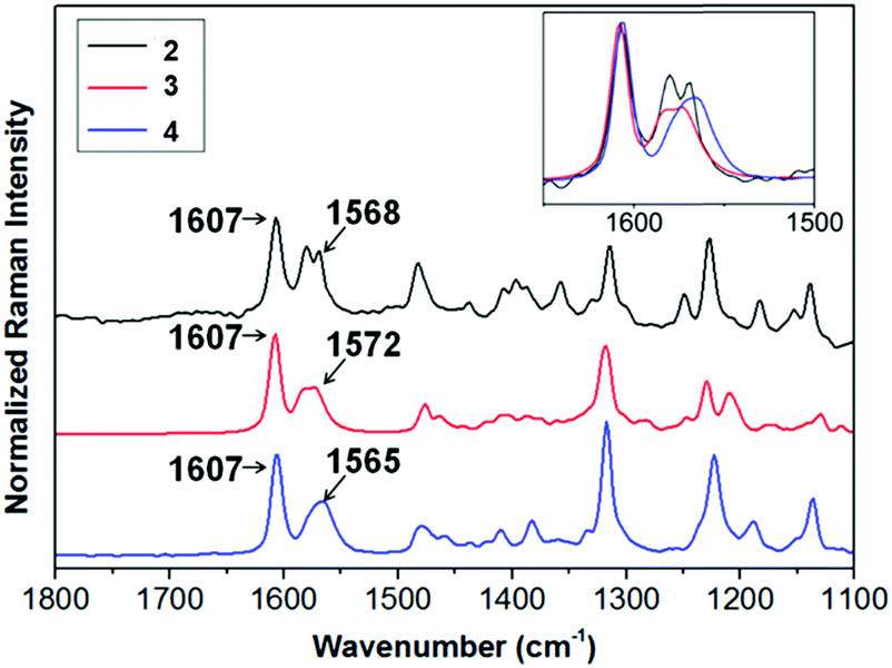 | ||
| Fig. 2 Comparison of the FT-Raman spectra normalized with respect to the 1607 cm−1 band, recorded for 2, 3 and 4. Inset: Zoom of the 1650–1500 cm−1 region. | ||
Self-assembly and crystal structure
The influence of the lengths of the alkyl chains on the self-assembly tendencies of these molecules was initially investigated using Field Emission Scanning Electron Microscopy (FE-SEM). Dip-coating of a substrate in a CH2Cl2![[thin space (1/6-em)]](https://www.rsc.org/images/entities/char_2009.gif) :CH3CN (1:1) solution of 2 renders highly aligned microwires that can reach a length up to some centimetres and only a few micrometers of diameter as could be determined using scanning electron microscopy (Fig. 3a). As can be observed in the inset of Fig. 3a, the wires show a perfect hexagonal cross-section. The formation of crystals of 3 and 4 can be readily accomplished by aging a CH2Cl2:CH3CN (1:1) solution of each compound for a few minutes until a turbidity is clearly observed. The resulting aggregates were deposited on a silicon substrate and visualized using a FE-SEM.
:CH3CN (1:1) solution of 2 renders highly aligned microwires that can reach a length up to some centimetres and only a few micrometers of diameter as could be determined using scanning electron microscopy (Fig. 3a). As can be observed in the inset of Fig. 3a, the wires show a perfect hexagonal cross-section. The formation of crystals of 3 and 4 can be readily accomplished by aging a CH2Cl2:CH3CN (1:1) solution of each compound for a few minutes until a turbidity is clearly observed. The resulting aggregates were deposited on a silicon substrate and visualized using a FE-SEM.
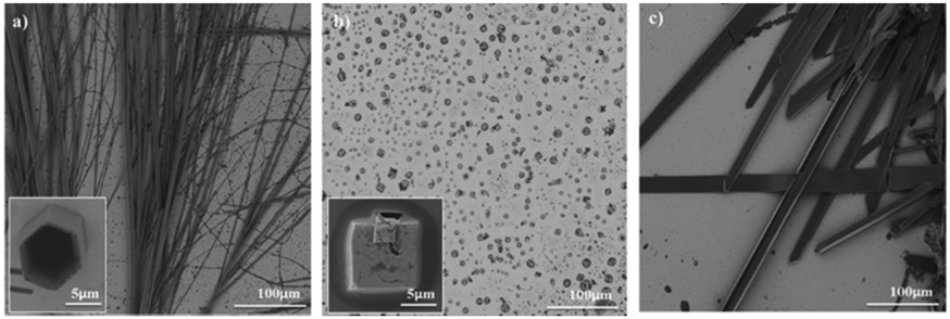 | ||
| Fig. 3 (a) Images of the crystalline structures of 2 (inset: view of the cross section) formed by dip-coating a silicon substrate on a concentrated 1:1 CH2Cl2:CH3CN solution. (b and c) Images of the crystalline structures of 3 (two different amplifications), and 4 obtained by ageing a 1:1 CH2Cl2:CH3CN solution of the corresponding compound and deposition of the crystalline material formed on a silicon substrate. | ||
The images show that the size of the alkyl chains has a dramatic influence on the crystalline characteristics of these compounds: thus, while compounds 2 and 4 show a preference to grow into anisotropic shapes forming long crystalline wires or microbelts, the tributyl derivative (3) grow as cubes.
In order to gain insight into the origin of these different crystalline characteristics and macroscopic morphologies, we have obtained crystals with sufficient sizes and quality for X-ray single crystal analysis of 3 and 4 by slow evaporation of 1:1 CH2Cl2:CH3CN solutions of the corresponding compounds. The crystal structure of 2 has been previously reported by us.13 Simulated powder diffraction patterns of the bulk crystals of 2–4 match well with those obtained for the aggregates deposited on substrates confirming that they correspond to the same crystal phase (see Fig. S5–S7, ESI†). An analysis of the crystal packing shows that compounds 2 and 4 crystallize as columnar assemblies, favouring the one-dimensional macroscopic growth; in sharp contrast, the tributyl derivative 3 crystallizes as dimers that pack in a herringbone-like array resulting in no preferred growth direction.
To understand the origin of these different packing tendencies we have traced how molecules interact with each other by establishing close contacts in the structures.
In the crystals, of 2, molecules pack forming stacks along the crystallographic c-axis (Fig. 4) which is coincident with the longest dimension of the crystal. In the structure of 2, each methyl group is involved in CH–π interactions with the aromatic rings that lie above and below it (contact distances: 2.935 Å and 2.985 Å). Fig. 5a depicts the unique interactions of 2, but considering the hexagonal symmetry of the crystals, all the methyl groups are involved in the stabilization of the column.
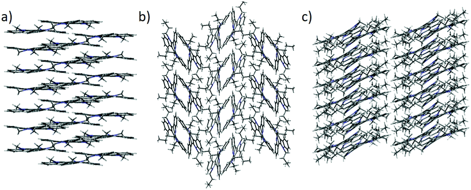 | ||
| Fig. 4 Different crystal packings shown by (a) 2 view along (a and b) 3 view along (a, and c) 4 view along b. | ||
 | ||
| Fig. 5 Depiction of the intermolecular CH–π interactions that stabilize the arrangement into columns of (a) 2 and (b) 4 (ring centroids are represented as red balls). Only unique interactions are shown, but the packing is stabilized by a number of additional interactions related by crystal symmetry. | ||
It should be noted that although these types of interactions are individually quite weak, their effects are additive and therefore their influence can be really powerful.21,22 This network of interactions explains the one-dimensional growth of these molecules. It has long been accepted that the growth rate of a facet is directly related to its attachment energy, which is considered as the energy necessary to split a slide of a facet. In this case cooperative interactions can be observed along the [001] direction crossing the most energetic plane.23 No interaction can be observed which would justify the growth direction of other facets of the crystal.24,25
By elongating the chain, we increase the number of potential CH-donors resulting in the columnar slipped arrangement found in the crystallographic packing of 4. In fact, as shown in Fig. 5b, in this derivative, one of the alkyl chains of the molecule interacts with different 5 and 6 membered rings of the heptacyclic platform below it (contact distances: 2.820 Å, 2.810 Å, 2.713 Å and 2.774 Å) while another chain is involved in several CH–π interactions with the molecule located above it (contact distances: 2.599 Å and 3.049 Å). Again no interactions can be traced between different stacks, which explains the anisotropic growth of these structures.
Molecules of 3 arrange in the crystal as dimers that pack in a herringbone-like array. The different packing tendency exhibited by 3 can also be ascribed to the cooperation of a number of CH–π interactions. An analysis of the close contacts in its crystal packing evidences that each molecule interacts with the other component of the dimer (contact distances: 2.621 Å and 2.981 Å) but also with molecules of two adjacent dimers (contact distances: 2.714 Å) placed in planes above and below. These results in a 3D network of interactions which would explain the cube-like morphology observed (Fig. 6).
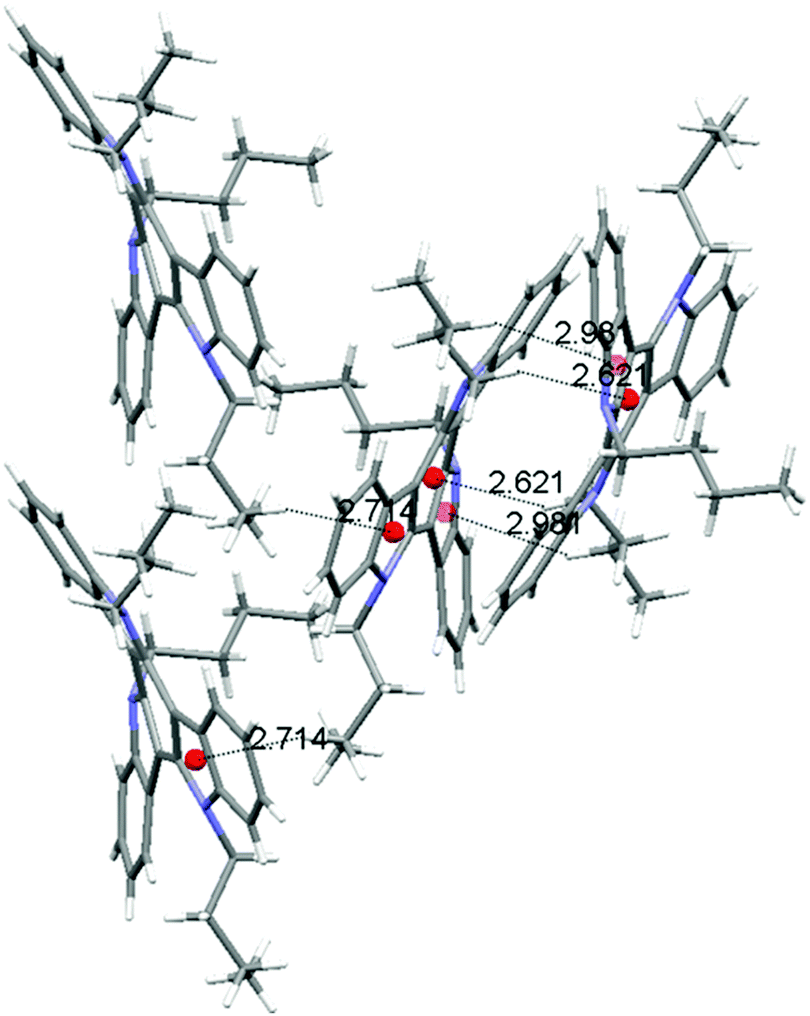 | ||
| Fig. 6 Depiction of the intermolecular CH–π interactions established between the molecules of 3 within the dimers and among neighboring dimers (ring centroids are represented as red balls). Only unique interactions are shown, but the packing is stabilized by a number of additional interactions related by crystal symmetry. | ||
Electrical characterization and charge transport parameters
On the basis of the evidence of different crystal packings and crystal morphologies, determined by diverse alkyl chains, and considering the acceptable mobility values observed for 2 as previously determined by SCLC13 and FET15 measurements, we have fabricated field effect transistors of 3 and 4 to gather information on how the length of the alkyl chains influences the electrical performance.To this end, 3 and 4-based field effect transistors with a vacuum-deposited active layer in standard bottom gate-top contact architecture were fabricated. Prior to device fabrication the active films were characterized using X-ray diffraction techniques. Simulated powder diffraction patterns of the bulk crystals of N-tributyltriindole (3) and N-trihexyltriindole (4) match well with those obtained for the thermal sublimed thin films, as determined using grazing incidence X-ray diffraction (GIXRD). Fig. 7 shows the comparison between the simulated power diffraction data and the GIXRD spectra of sublimed films of 4 on bare Si/SiO2 substrates, chosen as a reference. Note that only two peaks are observed in the experimental spectrum, corresponding to the ones indexed as (100) and (300) in the simulated spectrum, which indicates a highly aligned crystalline film with the columns parallel to the surface.
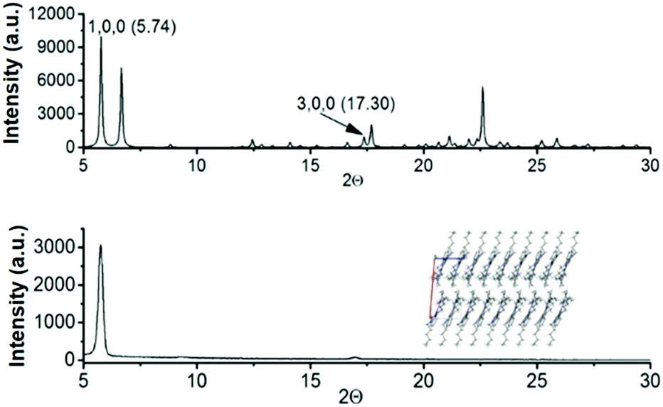 | ||
| Fig. 7 Powder X-ray diffractograms obtained from the single crystal data (above) and the experimental GIXRD of N-trihexyltriindole 4 deposited by slow sublimation under vacuum conditions (below). The inset images show the molecular packing in the thin films, with the plane (100) that indicates the orientation of the molecules parallel to the substrate. | ||
Curiously, only the devices fabricated with N-hexyltriindole 4 were active, despite its less conjugated skeleton as evidenced using Raman spectroscopy. This highlights the importance of a favourable supramolecular arrangement for achieving efficient charge transport. Note that the alkyl chain length not only affects the molecular structure but also significantly influences crystal packing as demonstrated in the previous section.
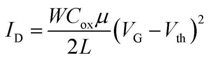
Fig. 8 shows the transfer and output characteristics of 4-based devices. Charge transport evaluation was carried out via analysis of the OFET current–voltage response in the saturation regime with the hypothesis of conventional transistor theory, following eqn:
 | ||
| Fig. 8 (a) Transfer characteristics of N-hexyltriindole 4 measured at a source–drain voltage of −80 V. (b) Output curves of N-hexyltriindole measured at gate voltages from 20 to −80 V in intervals of 20 V. | ||
These conditions were chosen after evaluating different temperatures and surface treatments that, as can be observed in Table 1, induce important differences in the extracted electrical data. Thus, higher preheating temperature results into two orders of magnitude lower mobility while devices deposited on HMDS substrates were inactive and those devices deposited on bare Si/SiO2 substrates presented hole mobilities one order of magnitude lower.
| Subst. treatment | Substrate temp. (°C) | μ (cm2 V−1 s−1) | V T (V) | I ON/IOFF |
|---|---|---|---|---|
| OTS | 80 | 2.8 × 10⁻⁴ | −27 | 8 × 10² |
| 60 | 3.0 × 10⁻² | −34 | 2 × 10⁴ | |
| 25 | 1.7 × 10⁻² | −6 | 2 × 10⁴ | |
| HMDS | 80 | N.A. | N.A. | N.A. |
| 60 | N.A. | N.A. | N.A. | |
| 25 | N.A. | N.A. | N.A. | |
| No treatment | 80 | N.A. | N.A. | N.A. |
| 60 | 2.4 × 10⁻³ | −21 | 2 × 10⁴ | |
| 25 | 4.6 × 10⁻⁵ | −2 | 7 × 101 | |
To understand the differences observed in the mobility values obtained under different conditions, the effects of temperature and surface treatment on thin film crystallinity and morphology were evaluated with the help of AFM. Thermal treatments were performed at temperatures significantly below the melting points (see the corresponding differencial scanning calorimetry traces in Fig. S8, ESI†), thus temperature induced differences expected to derive from morphological changes. As shown in Fig. 9 for OTS-treated substrates, belt-like structures similar to those found in single crystals are recorded for 60 °C temperature, while on bare and HMDS-treated substrates, round-like grains are formed, which are less efficient for charge transport. Note that the non active or poorly performing films, either deposited on HMDS-treated substrates and/or deposited at high temperatures, show a remarkable roughness of 0.5–2 μm s, which probably contributes to the low performances.
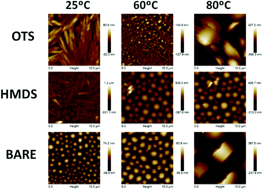 | ||
| Fig. 9 Tapping mode AFM images (10 μm × 10 μm) of thermally evaporated 4-films on substrates preheated at the indicated temperatures. OTS: octadecyltrichlorosilane- and HMDS: hexamethyldisilazane-treated substrates. | ||
In an attempt to give a step forward to the practical applications of these materials, OFETs were also fabricated by drop-casting ∼2.5 mg ml−1 solutions of 2–4 in chloroform. Again only devices prepared with semiconductor 4 as an active layer presented the field effect behaviour. Curiously in spite of the good results previously obtained for 2 in evaporation processed OFETs, solution processed devices prepared with this compound were inactive, probably due to the formation of poor quality films; AFM images indicate the appearance of non well-interconnected crystalline wires, probably hindering efficient charge transport between wires in the device channel (Fig. S7, ESI†). In contrast, AFM images of solution processed 4 samples show quite homogeneous films, highlighting the remarkable processability modulation by increasing the N-alkyl chain length from methyl to hexyl groups.
Prior to device fabrication, the active films were again characterized using X-ray diffraction techniques. The GIXRD spectrum recorded for film 4 rendering the best performance in OFETs shows, as in sublimed films, two peaks corresponding to the ones indexed as (100) and (300) in the simulated spectrum, indicating comparable crystalline phases (Fig. S8, ESI†).
Hole mobilities of up to 6.4 × 10⁻³ cm2 V−1 s−1 with a threshold voltage of ∼−31 V were obtained for a 4-based OFET annealed at 80 °C, with a bottom gate-top contact architecture, and using HMDS-treated Si/SiO2 substrates as gate/dielectric layers (see Table 2). Note that despite the fact that this value is around one order of magnitude smaller than the values recorded for vacuum-deposited films, to the best of our knowledge this is the highest value reported so far for solution processed triindole-based semiconductors in organic field effect transistors.
| Subst. treatment | Annealing temp. (°C) | μ (cm2 V−1 s−1) | V T (V) | I ON/IOFF |
|---|---|---|---|---|
| OTS | 120 | 4.5 × 10⁻⁴ | −32 | 1 × 10⁴ |
| 80 | 1.5 × 10⁻³ | −37 | 2 × 10³ | |
| 60 | 1.7 × 10⁻³ | −38 | 4 × 10⁴ | |
| HMDS | 80 | 6.4 × 10⁻³ | −31 | 3 × 10³ |
| 60 | 2.6 × 10⁻³ | −12 | 5 × 10² | |
In order to rationalize the effect of the length of the N-alkyl chains on the charge transport properties of triindoles we have theoretically predicted the fundamental charge transport parameters, such as intramolecular reorganization energies (λh), electronic coupling (or transfer integrals) and mobilities. As expected, the structural reorganization needed to accommodate a charge is not affected by the length of the N-alkyl groups and very similar λh values are found for 2–4 (∼235 meV). However, significant differences are found when comparing the transfer integrals for hole transport (th) for dimers extracted from the experimental single crystal data of 2–4. Our results show: (i) larger th values for 2 (−41 meV), which is driven by efficient HOMO–HOMO overlap due to its intermolecular columnar organization. (ii) Slightly lower th values (−28 meV) for dimers along the columns of 4, with the slipped columnar arrangement and the larger number of CH–π interactions likely decreasing wave function overlap. (iii) Moderate th values (−23 meV) between cofacial dimers of 3 extracted from the crystal, with th values that drop to −3 meV between molecules of two adjacent dimers in a herringbone-like configuration. This result underlines the strong impact of the intermolecular packing on the transport properties. Considering that the calculated reorganization energies in triindoles 2–4 are much larger than the electronic coupling, charge localization takes place and transport is expected to occur via a charge-hopping mechanism. We calculated the intrinsic hole mobilities by assuming the charge hopping regime in the context of the semiclassical Marcus theory.26 Mobilities of 0.140 and 0.067 cm2 V−1 s−1 were estimated for 2 and 4 (note the good agreement between experimental and theoretical values for 4, being 0.03 and 0.067 cm2 V−1 s−1 respectively).
Experimental
SEM Characterization
Scanning electron microscopy (SEM) images were obtained on a Nova NanoSEM 230 FEI field-emission scanning electron microscope using a vCD detector operating at low pressure with an accelerating voltage of 5 kV.X-ray structure
A colorless crystal of 3 showing well defined faces were mounted on a Bruker Smart CCD diffractometer equipped with a normal focus, 2.4 kW sealed-tube X-ray source (MoKα radiation, λ = 0.71067 Å) operating at 50 kV and 30 mA. Data were collected over a hemisphere of the reciprocal space by a combination of three exposure sets. Each exposure of 10 s covered 0.3° in ω over the range 2.5° <θ < 28°. The first 100 frames were recollected at the end of the data collection to monitor crystal decay.A colorless crystal of 4 showing well defined faces was mounted on a Bruker four circle kappa-diffractometer equipped with a Cu INCOATED microsource, operated at 30 W power (45 kV, 0.60 mA) to generate CuKα radiation (λ = 1.54178 Å), and a Bruker VANTEC 500 area detector (microgap technology). Diffraction data were collected exploring over a hemisphere of the reciprocal space in a combination of φ and ω scans to reach a resolution of 0.86 Å, using a Bruker APEX2 software suite (each exposure of 40 s covered 1o in ω or φ). Unit cell dimensions were determined for the least-squares fit of reflections with I > 20σ. A semi-empirical absorption and scale correction based on equivalent reflection was carried out using SADABS APEX. The structures were solved using direct methods. The final cycles of refinement were carried out by full-matrix least-squares analyses with anisotropic thermal parameters of all non-hydrogen atoms. The hydrogen atoms were fixed at their calculated positions using distance and angle constraints. All calculations were performed using SMART27 and APEX228 software for data collection and for data reduction; SHELXS29 and SHELXL30 to resolve and refine the structures using Olex2.31 CCDC 1021612 and 1446933 for 3 and 4 respectively.†
Vibrational spectroscopy
FT-Raman spectra with 1064 nm excitation were recorded using a FT Raman accessory kit (RamII) of a Bruker Vertex 70 FT-IR interferometer and a continuous-wave Nd:YAG laser. A germanium detector working at liquid-nitrogen temperature was used, the Raman scattering radiation being collected in a back-scattering configuration with a 4 cm−1 spectral resolution. An average of 1000 scans was used in the reported spectra.OFET fabrication
Field effect transistors were fabricated with a vacuum-deposited active layer or solution-processed film in a standard bottom gate-top contact architecture. First, the gate/dielectric substrates (Si/300 nm SiO2) were double-cleaned in an ultrasonic bath with ethanol prior to drying under a flow of nitrogen. Next, the surface was functionalized with a self-assembled monolayer of either hexamethyldisilazane (HMDS) or octadecyltrichlorosilane (OTS) to minimize interfacial trapping sites.32 Then, thin films of 2–4 were prepared by slow sublimation under vacuum conditions on preheated substrates at different temperatures or by drop casting a 2.5 mg ml−1 solution in chloroform, followed by an annealing treatment. Finally, 30 nm gold source and drain electrodes were thermally evaporated through a shadow mask. Devices were tested under vacuum by using an EB-4 Everbeing probe station with a 4200-SCS/C Keithley semiconductor characterization system and a customized vacuum probe station.DFT calculations
The molecular geometries of the neutrals and radical-cation states of compounds 2–4 were calculated at the Density Functional Theory (DFT) level using the hybrid, generalized gradient approximation (GGA) functional B3LYP33,34 and a 6-31G** basis35,36 set, as implemented in the GAUSSIAN09 program.37 For the neutral state C3 symmetry constraints were imposed for triindoles 2–4 during the optimization processes. On the resulting ground-state optimized geometries, harmonic frequency calculations were performed to ensure the finding of the global minimum. The reorganization energies associated with hole transfer were calculated directly from the relevant points on the potential energy surfaces using the standard procedure detailed in the literature.38The HOMO transfer integrals (tHomo,Homo, referred to in the text as th) for the nearest-neighbour pairs of molecules taken out of the 2–4 crystal structures were calculated at the B3LYP/6-31G(d,p) level, according to the approach described by Valeev et al.39 with the corresponding matrix elements evaluated with Gaussian 09. Note that the coupling values depend on the functional used and generally increase with the increasing percentage of Hartree–Fock exchange in the functional.40 For molecule 2, where a two-fold degenerate HOMO is observed on isolated molecules at the geometry of the crystal, the HOMO−1 transfer integrals (tHomo−1) were also calculated in order to recalculate average th values as [(tHomo,Homo2+ tHomo−1,Homo−12 + tHomo−1,Homo2 + tHomo,Homo−12)/2]1/2. However, no difference is found between the average th values and the previously calculated tHomo,Homo values.
Conclusions
The relationship between the length of the N-alkyl chains and organizational preferences and device performance of a series of N-trialkyl triindoles has been investigated through an experimental and theoretical approach. We have found that the length of the N-alkyl chains in this semiconducting platform strongly influences on how these molecules interact with each other in bulk materials and points towards cooperative CH–π interactions in the origin of the different superstructures observed. The results of this study highlight the extreme impacts that subtle modifications in the triindole platform have on device performance and show that through an adequate functionalization we can modulate both material processability and supramolecular organization towards its incorporation into OFETs. In particular, the application of N-trihexyltriindoles in evaporated OFETs presenting mobilities of around 0.03 cm2 V−1 s−1 and in solution processed devices showing comparable metrics confirms triindole-based molecules as promising easy-to-process hole transport materials.Conflicts of interest
There are no conflicts to declare.Acknowledgements
This work was financially supported by the MINECO of Spain (CTQ2015-66897, MAT2016-78465-R and CTQ2016-78557-R) and the Comunidad de Madrid S2013/MIT-2740 and Junta de Andalucía (FQM-159).Notes and references
- H. Klauk, Organic Electronics: Materials, Manufacturing and Applications, Wiley-VCH, Weinheim, 2006 Search PubMed.
- H. Klauk, Organic Electronics: More Materials and Applications, Wiley-VCH, Weinheim, 2012 Search PubMed.
- Special issue on π-functional materials for organic electronics: Chem. Mater., 2011, 23, 309–922.
- M. Mas-Torrent and C. Rovira, Chem. Rev., 2011, 111, 4833–4856 CrossRef CAS PubMed.
- J. Mei, Y. Diao, A. L. Appleton, L. Fang and Z. Bao, J. Am. Chem. Soc., 2013, 135, 6724–6746 CrossRef CAS PubMed.
- C. Wang, H. Dong, W. Hu, Y. Liu and D. Zhu, Chem. Rev., 2012, 112, 2208–2267 CrossRef CAS PubMed.
- C. Ruiz, E. García Frutos, G. Hennrich and B. Gómez-Lor, J. Phys. Chem. Lett., 2012, 3, 1428–1436 CrossRef CAS PubMed.
- E. R. T. Tiekink, The Importance of π-Interactions in Crystal Engineering: Frontiers in Crystal Engineering, John Wiley & Sons, Ltd, Chichester, UK, 2012 Search PubMed.
- L. M. Salonen, M. Ellermann and F. Diederich, Angew. Chem., Int. Ed., 2011, 50, 4808–4842 CrossRef CAS PubMed.
- G. R. Desiraju, J. Am. Chem. Soc., 2013, 135, 9952–9967 CrossRef CAS PubMed.
- S. E. Wheeler and J. W. G. Bloom, J. Phys. Chem. A, 2014, 118, 6133–6147 CrossRef CAS PubMed.
- E. M. García-Frutos, G. Hennrich, E. Gutierrez, A. Monge and B. Gómez-Lor, J. Org. Chem., 2010, 75, 1070–1076 CrossRef PubMed.
- E. M. García-Frutos, E. Gutierrez-Puebla, M. A. Monge, R. Ramírez, P. D. Andrés, A. D. Andrés, R. Ramírez and B. Gómez-Lor, Org. Electron., 2009, 10, 643–652 CrossRef.
- A. Benito-Hernández, U. K. Pandey, E. Cavero, R. Termine, E. M. García-Frutos, J. L. Serrano, A. Golemme and B. Gómez-Lor, Chem. Mater., 2013, 25, 117–121 CrossRef.
- M. Reig, J. Puigdollers and D. Velasco, J. Mater. Chem. C, 2015, 3, 506–513 Search PubMed.
- R. A. Valentine, A. Whyte, K. Awaga and N. Robertson, Tetrahedron Lett., 2012, 53, 657–660 CrossRef CAS.
- The only contribution reported to date on triindole-based solution processed thin film transistors (OFETs) is for a triphenylene-fused triindole systems with hole mobility determined of 10−4 cm2 V−1 s−1: C. Ruiz, U. K. Pandey, R. Termine, E. M. García-Frutos, G. López-Espejo, R. P. Ortiz, W. Huang, T. J. Marks, A. Facchetti, M. C. Ruiz Delgado, A. Golemme and B. Gómez-Lor, ACS Appl. Mater. Interfaces, 2016, 8, 26964–26971 CAS.
- M.-S. Yuan, T.-B. Li, W.-J. Wang, Z.-T. Du, J.-R. Wang and Q. Fang, Spectrochim. Acta, Part A, 2012, 96, 1020–1024 CrossRef CAS PubMed.
- W. Y. Lai, Q. Y. He, R. Zhu, Q. Q. Chen and W. Huang, Adv. Funct. Mater., 2008, 18, 265–276 CrossRef CAS.
- C. Ruiz, E. García Frutos, D. A. da Silva Filho, J. López Navarrete, M. C. Ruiz Delgado and B. Gómez-Lor, J. Phys. Chem. C, 2014, 118, 5470–5477 CAS.
- M. Nishio, M. Hirota and Y. Umezawa, The CH/π interaction. Evidence, Nature and Consequences, Wiley-VCH, New York, 1998 Search PubMed.
- M. Nishio, CrystEngComm, 2004, 6, 130–158 RSC.
- A. Bacchi, G. Cantoni, D. Cremona, P. Pelagatti and F. Ugozzoli, Angew. Chem., Int. Ed., 2011, 50, 3198–3201 CrossRef CAS PubMed.
- F. R. Massaro, M. Moret, M. Bruno and D. Aquilano, Cryst. Growth Des., 2013, 13, 1334–1341 CAS.
- P. Hartman and P. Bennema, J. Cryst. Growth, 1980, 49, 145–156 CrossRef CAS.
- R. A. Marcus, Rev. Mod. Phys., 1993, 65, 599–610 CrossRef CAS.
- Software for the SMART system, V.5.04, Bruker-Siemens Analytical X-ray Instruments, Inc., Madison, WI, USA, 1998 Search PubMed.
- APEX2, Bruker-AXS, Madison, WI, 2006 Search PubMed.
- G. Sheldrick, Acta Crystallogr., Sect. A: Found. Crystallogr., 2008, 64, 112–122 CrossRef CAS PubMed.
- G. Sheldrick, Acta Crystallogr., Sect. C: Cryst. Struct. Commun., 2015, 71, 3–8 CrossRef PubMed.
- O. V. Dolomanov, L. J. Bourhis, R. J. Gildea, J. A. K. Howard and H. Puschmann, J. Appl. Crystallogr., 2009, 42, 339–341 CrossRef CAS.
- M.-H. Yoon, C. Kim, A. Facchetti and T. J. Marks, J. Am. Chem. Soc., 2006, 128, 12851–12869 CrossRef CAS PubMed.
- A. D. Becke, J. Chem. Phys., 1993, 98, 5648–5652 CrossRef CAS.
- C. T. Lee, W. T. Yang and R. G. Parr, Phys. Rev. B: Condens. Matter Mater. Phys., 1988, 37, 785–789 CrossRef CAS.
- P. C. Hariharan and J. A. Pople, Theor. Chim. Acta, 1973, 28, 213–222 CrossRef CAS.
- W. J. Hehre, R. Ditchfield and J. A. Pople, J. Chem. Phys., 1972, 56, 2257 CrossRef CAS.
- M. J. Frisch, et al., Gaussian 09, Wallingford, CT, 2009 Search PubMed.
- J.-L. Brédas, D. Beljonne, V. Coropceanu and J. Cornil, Chem. Rev., 2004, 104, 4971–5004 CrossRef PubMed.
- E. F. Valeev, V. Coropceanu, D. A. da Silva, S. Salman and J. L. Bredas, J. Am. Chem. Soc., 2006, 128, 9882–9886 CrossRef CAS PubMed.
- G. Sini, J. S. Sears and J.-L. Brédas, J. Chem. Theory Comput., 2011, 7, 602–609 CrossRef CAS PubMed.
Footnote |
| † Electronic supplementary information (ESI) available: Cyclic voltamograms and UV spectra of 2–3, DFT theoretical eigenvectors for the Raman bands and GIXRD and AFM of solution processed films, explanation to checkCIF alerts. CCDC 1021612(3) and 1446933(4). For ESI and crystallographic data in CIF or other electronic format see DOI: 10.1039/c7tc03866f |
| This journal is © The Royal Society of Chemistry 2018 |