 Open Access Article
Solution-processed Er3+-doped As3S7 chalcogenide films: optical properties and 1.5 μm photoluminescence activated by thermal treatment
L.
Strizik†
 *a,
T.
Wagner†
 *ab,
V.
Weissova
a,
J.
Oswald
 c,
K.
Palka
 ab,
L.
Benes
d,
M.
Krbal
 b,
R.
Jambor
a,
C.
Koughia
e and
S. O.
Kasap
 e
e
aDepartment of General and Inorganic Chemistry, University of Pardubice, Studentska 573, 53210 Pardubice, Czech Republic. E-mail: lukas.strizik@upce.cz; tomas.wagner@upce.cz; Tel: +420-466037000 Tel: +420-466037144
bCenter of Materials and Nanotechnologies, University of Pardubice, nam. Cs. legii 565, 53002 Pardubice, Czech Republic
cInstitute of Physics of the AS CR, v.v.i., Cukrovarnicka 10, 16200 Prague, Czech Republic
dJoint Laboratory of Solid State Chemistry, University of Pardubice, Studentska 95, 53210 Pardubice, Czech Republic
eDepartment of Electrical Engineering, University of Saskatchewan, Campus Dr. 57, Saskatoon, Canada
First published on 24th July 2017
Abstract
We report on the optical properties of Er-doped As3S7 chalcogenide films prepared using the two step dissolution process utilizing the As3S7 glass dissolved with propylamine and by further addition of the tris(8-hydroxyquinolinato)erbium(III) (ErQ) complex acting as an Er3+ precursor. Thin films were deposited by spin-coating, thermally stabilized by annealing at 125 °C and further post-annealed at 200 or 300 °C. The post-annealing of films at 200 °C and 300 °C densifies the films, improves their optical homogeneity, and moreover activates the Er3+:4I13/2 → 4I15/2 (λ ≈ 1.5 μm) PL emission at pumping wavelengths of 808 and 980 nm. The highest PL emission intensity was achieved for As3S7 films post-annealed at 300 °C and doped with ≈1 at% of Er which is beyond the normal Er3+ solubility limit of As–S melt-quenched glasses. The solution-processed deposition of the rare-earth-doped chalcogenide films utilizing the organolanthanide precursors has much potential for application in printed flexible optoelectronics and photonics.
Introduction
Rare-earth(RE)-doped chalcogenide glasses (ChGs) have attracted attention due to their application in optoelectronics and photonics such as optical amplifiers,1–3 waveguides,4,5 sensors,6–8 displays,9–11 and bioimaging devices.12 Chalcogenide glasses have the advantage that they can be fabricated in arbitrary shapes.13 In contrast to amorphous oxides and fluorides, ChGs are covalently bonded semiconductors,14,15 which leads to their broad transparency from the visible to mid-infrared spectral region and large linear and nonlinear refractive index.13 These unique properties singled them out as good host matrices for RE3+ ions due to suppressed multiphonon relaxation and enhanced optical confinement and radiative recombination.13,16,17Another interesting area of research has been the fabrication of amorphous chalcogenide films, which can be relatively easily prepared using straight forward physical vapor deposition techniques18 and some of them using sol–gel processes such as spin-coating.19–26 Above all, the solution-based processing of chalcogenides allows their printing onto flexible substrates, which significantly expands their applicability.24–36 However, the solubility of chalcogenides is limited due to their covalent bonding.37 There have been several reports on deposition of chalcogenides using solution-based processes, utilizing NH2-based solvents (propylamine and hydrazine);19,24–26,35–37 sometimes in combination with SH-based (ethanedithiol) solvents.38 However, poor solubility (slurry formation) or inertness of the RE-doped chalcogenides to NH2-based solvents basically prevents them from forming homogenous solutions. Moreover, it should be mentioned that the RE-doped melt-quenched ChGs usually contain Ga which improves the solubility of RE ions39 from ∼0.1 at% (e.g. As2S3:Er40) to ∼1 at% (e.g. Ge–Ga–Se:Er41). Unfortunately, the solubility of RE-doped ChGs containing Ga in NH2-based solvents is still as poor as ChGs without Ga.
To the best of our knowledge, to date there has been no report on the compact RE-doped chalcogenide films prepared using the sol–gel process (except for quantum dots42). In this work, we demonstrate a two-step solution-processed deposition of the RE-doped chalcogenide films which can overcome the aforementioned difficulty. First, an undoped As3S7 chalcogenide glass was dissolved with propylamine (PA) and second the tris(8-hydroxyquinoline)erbium(III) complex (ErQ) acting as a Er3+ precursor was added to the previous solution.
The Er3+ precursor ErQ has been chosen due to the following two reasons: (1) the Er3+-doped materials have been studied extensively due to the strong and sharp ≈1.5 μm photoluminescence emission matching the telecommunication C-band. Thus, one of the critical material issues for the C-band telecommunications is the highest achievable Er3+ solubility in a host matrix with a high photoluminescence performance.43 (2) The ErQ complex has been shown to be a promising material for organic light-emitting diodes (OLEDs)44,45 and the ≈1.5 μm optical amplifiers.44,46–49
We demonstrate that the use of organolanthanide precursors allows one to incorporate higher concentrations of RE ions into chalcogenides (∼1 at% Er in As3S7) in comparison with the RE-doped melt-quenched glasses (∼0.1 at% Er in As2S3).40 The optical properties and the 4I13/2 → 4I15/2 photoluminescence (PL) emission at ≈1.5 μm of the As3S7:ErQ films annealed at 125, 200 or 300 °C are presented. Annealing of the As3S7:ErQ films leads to the activation of the ≈1.5 μm PL emission and an improvement of the optical homogeneity of the films. The strongest ≈1.5 μm PL emission was observed in As3S7 films annealed at 300 °C containing ≈1 at% of Er3+ which is beyond the Er3+ solubility limit of the melt-quenched As–S glass.40
The present work that utilizes the dissolution of pure chalcogenide glasses and the organolanthanide precursors of RE3+ ions opens up a new route for the manufacturing of functional RE-doped chalcogenides using the low-cost and low-temperature solution-based deposition process.
Experimental
Synthesis of As3S7 bulk glass
As3S7 chalcogenide glass was synthesized using the standard melt-quenching technique from high purity elements of As (5N) and S (4N5) which were weighted under an inert atmosphere of N2 in a glove box with concentrations of H2O and O2 < 1 ppm. An ampoule loaded with raw elements (10 g batch) was sealed at a pressure of ∼10−3 Pa and heated in a rocking furnace at 650 °C for 12 h. The As3S7 glass was then obtained by the quenching of the ampoule with melt in air.Preparation of solutions
1 g of the crushed As3S7 glass was dissolved with 6 mL of propylamine (PA); Sigma-Aldrich, 98% purity, CAS: 107-10-8. Then, the Er3+ precursor was added in the form of the commercially available tris(8-hydroxyquinolinato)erbium(III) complex; Sigma-Aldrich, 97% purity, CAS: 23606-16-8. These mixtures were filtered through a 0.23 μm syringe filter to remove possible big particles. Three yellow-orange PA solutions were prepared: (I) As3S7, (II) As3S7/ErQ = 20 roughly corresponding to As3S7:5 mol% ErQ, and (III) As3S7/ErQ = 10 roughly corresponding to As3S7:10 mol% ErQ, where As3S7/ErQ is the molar ratio (mol/mol).Deposition of thin films
As3S7:ErQ films were deposited by a spin-coating technique using the above mentioned PA solutions. The deposition was carried out by dropping of ≈300 μL of the solution onto pre-cleaned microscopic glasses (25 × 25 mm2) followed by a three-step spinning protocol: (1) spreading out the solution over a substrate by spinning at a spin speed of 500 rpm for 10 s, and an acceleration of 300 rpm2, (2) deposition of the films at 3000 rpm for 30 s and an acceleration of 4000 rpm2, and (3) final drying of the deposited films at 750 rpm for 10 s and an acceleration of 10![[thin space (1/6-em)]](https://www.rsc.org/images/entities/char_2009.gif) 000 rpm2. The as-deposited chalcogenide films were stabilized by annealing at 125 °C for 12 h under a reduced pressure of ≈10 Pa. Further post-annealing of the films was carried out under an inert Ar atmosphere at 200 °C for 30 min or at 300 °C for 5 min. The average thickness of the films is ≈3 μm. Table 1 presents the labelling of all the studied As3S7:ErQ films annealed at various temperatures.
000 rpm2. The as-deposited chalcogenide films were stabilized by annealing at 125 °C for 12 h under a reduced pressure of ≈10 Pa. Further post-annealing of the films was carried out under an inert Ar atmosphere at 200 °C for 30 min or at 300 °C for 5 min. The average thickness of the films is ≈3 μm. Table 1 presents the labelling of all the studied As3S7:ErQ films annealed at various temperatures.
As3S7![[thin space (1/6-em)]](https://www.rsc.org/images/entities/char_2009.gif) : :![[thin space (1/6-em)]](https://www.rsc.org/images/entities/char_2009.gif) ErQ ratio (mol%) ErQ ratio (mol%) |
Annealing temperature (°C) | ||
|---|---|---|---|
| 125 | 200 | 300 | |
| Undoped | 0ErQ-125 | 0ErQ-200 | 0ErQ-300 |
| 20 | 5ErQ-125 | 5ErQ-200 | 5ErQ-300 |
| 10 | 10ErQ-125 | 10ErQ-200 | 10ErQ-300 |
Characterization methods
The amorphous vs. crystalline state of the deposited films was investigated by the X-ray diffraction (XRD) analysis using the Bruker AXS D8-Advance with Cu Kα radiation and a secondary graphite monochromator in the range of 2θ from 10° to 65°. The chemical composition was analyzed at an acceleration voltage of 20 kV using an energy-dispersive X-ray (EDX) microanalyzer AZtec X-Max 20, Oxford Instruments, which is a part of the scanning electron microscope LYRA 3, Tescan. The films for EDX spectroscopy were overcoated by a very thin (≈10 nm) film Cr to ground the sample during the EDX measurements. The microscopic homogeneity of the films was studied using an Olympus optical microscope, modelBX51TF. The transmittance of both the As3S7:ErQ PA solutions and the deposited films was measured using a double-beam UV-Vis-NIR spectrophotometer Jasco V-570 in the spectral region of wavelength λ from 400 to 2500 nm with a 2 nm step. The transmittance measurements of the PA solutions were carried out in SiO2 cuvettes with an optical path of 10 mm. Absorption coefficients and refractive indices of the thin films were determined using a modified Swanepoel method.50–52 Spectral dependence of transmittance T(λ) of a uniform film on the substrate can be expressed as: | (1) |
 | (2) |
When the films exhibit nonuniformity not only in the thickness but also in n, and also exhibit scattering (e.g. due to voids or inclusions) eqn (2) needs a new interpretation and modification. Firstly, the variation (gradation) of the refractive index through the thickness of the film can be solved by interpreting d and Δd as an effective thickness and an effective thickness variation, respectively. Secondly, when the light scattering effect is present, the absorption coefficient α of eqn (2) represents an effective loss coefficient composed of the absorption coefficient αabs and the scattering coefficient αsi.e., α = αabs + αs. To fit eqn (2) experimental T(λ) data, one needs to choose appropriate values of d and Δd as well as reasonable approximations for the spectral dependencies of all other parameters in the model i.e., n, αabs and αs. The one-pole Sellmeier equation (eqn (3)) has been used for the dispersion of the refractive index n(λ):53
 | (3) |
 | (4) |
| αs(E) = rE4, | (5) |
Overall, to fit the experimental data 9 parameters have been used: d, Δd, n0, BS, CS, Eg, ΔE, a and r. In addition to the Swanepoel method, the refractive index of the thin films was determined from spectroscopic ellipsometry experiments using a J.A. Woollam, Co Inc. instrument and VASE® software. Measurement was carried out in the spectral range of 0.54–2.0 eV with a 0.03 eV step and at angles of light incidence at 65°, 70° and 75°. Chalcogenide films were parameterized using the model “Substrate|Graded As3S7:ErQ Thin Film|Roughness”. The dispersion of the refractive index of the As3S7:ErQ films in the transparent spectral region was described using the Cauchy model n(λ) = AC + BC/λ2 + CC/λ4.55 However, in the case of films annealed at 200 °C and 300 °C, the additional Urbach absorption was added according to eqn (9) in ref. 56. The roughness layer is represented by the effective medium approximation according to Bruggeman composed of 50 vol% of voids and 50 vol% of As3S7:ErQ film.57 The good match between the experimental data and the chosen model was found when the As3S7:ErQ layer is graded in the refractive index. This observation corresponds with the outlined assumptions above for the Swanepoel analysis.
The Er3+:4I13/2 → 4I15/2 (λ ≈ 1.5 μm) PL emission spectra of the thin films were recorded using a photoluminescence spectroscope set-up at pumping wavelengths of 808 and 980 nm (an excitation power density of ≈9.5 W cm−2) using a 1/2 m double monochromator and a liquid nitrogen cooled Ge detector. The signal was processed through a computer-controlled preamplifier and a lock-in amplifier. The emission spectra were recorded in the spectral range of 1430 to 1650 nm with a 0.5 nm step and at room temperature.
Results and discussion
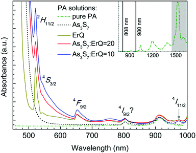
The absorption spectra of the PA, the PA + ErQ, the PA + As3S7 and the PA + As3S7 + ErQ solutions referenced to empty SiO2 cuvettes are presented in Fig. 1. PA itself possesses numerous absorption bands in the near infrared spectral region (inset of Fig. 1) with a strong absorption band at ≈1.5 μm which overlaps the spectral region of the Er3+:4I13/2 → 4I15/2 PL emission. Therefore, it is crucial to remove the PA solvent from the spin-coated films in order to obtain the intense ≈1.5 μm PL emission. The addition of As3S7 to the PA solvent leads to the appearance of the strong absorption roughly at λ ≈ 0.5 μm which originates from the fundamental absorption of the solvated As–S-based clusters.58 Further addition of ErQ to PA + As3S7 solution leads to the formation of new absorption bands centered approximately at ≈520, ≈545, ≈650 and ≈975 nm. These bands correspond to the Er3+ intra-4f ground state absorption (GSA) electronic transitions to 2H11/2, 4S3/2, 4F9/2 and 4I11/2 levels which is confirmed by the absorption spectrum of the PA + ErQ solution. However, the expected Er3+ GSA bands at ≈810 nm (4I9/2) and at ≈1.5 μm (4I13/2) are masked by the strong PA absorption.All spin-coated As3S7:ErQ thin films were thermally stabilized at 125 °C under a residual pressure of ≈10 Pa, resulting in yellow-orange films. The post-annealing of these films was carried out at 200 or 300 °C in an Ar inert atmosphere leading to their significant darkening (see photographs in Fig. 4). The 200 and 300 °C post-annealing temperatures were selected to be still below the softening temperature Ts ≈ 225 °C of the As3S7 glass59 and around the melting (decomposition) point Tm ≈ 300 °C of ErQ,60 respectively. Nevertheless, the optical microscopic inspection of the prepared films in Fig. 2 revealed that the ErQ-free As3S7 films were already damaged upon annealing at both post-annealing temperatures. Observed defects can be attributed to the evaporation of the volatile sulfide-based compounds such as H2S at temperatures above 150 °C.21 Strikingly, the ErQ-doped As3S7 films seem to be resistant to the thermal treatment with no significant evidence of surface damage after post-annealing, even at 300 °C.
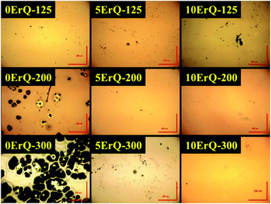 | ||
| Fig. 2 The optical microscopy photographs of the As3S7:ErQ spin-coated and annealed thin films; red bars correspond to size of 250 μm. | ||
The observed darkening of the post-annealed films at 200 °C or 300 °C can be related to (1) evaporation of the sulfur-based volatile compounds, (2) densification of the prepared films due to the removal of the PA solvent, and (3) to some extent to the decomposition of the ErQ complex. The first two cases are corroborated using EDX spectroscopy in Table 2 where one can see increasing As:S atomic ratio and decreasing nitrogen content in films with increasing annealing temperature. However, even annealing at 300 °C did not lead to PA-free films, which is in agreement with the previously reported results on spin-coated As–S21 and As–Se films.22 Moreover, the addition of ErQ to As3S7 increases the PA content in films probably due to the high binding affinity of PA for ErQ, but the exact mechanism remains unclear.
| Sample | As (at%) | S (at%) | N (at%) | Er (at%) | As:S (at%/at%) |
|---|---|---|---|---|---|
| 0ErQ-theor | 30.(0) | 70.(0) | 0 | 0 | 0.429 |
| 0ErQ-125 | 27.(8) | 63.(2) | 9.(0) | 0 | 0.440 |
| 0ErQ-200 | 30.(0) | 62.(8) | 7.(8) | 0 | 0.478 |
| 0ErQ-300 | — | — | — | — | — |
| 5ErQ-theor | 29.(4) | 68.(6) | 1.(5) | 0.(5) | 0.429 |
| 5ErQ-125 | 26.(5) | 60.(0) | 13.(2) | 0.(2) | 0.442 |
| 5ErQ-200 | 29.(6) | 59.(6) | 10.(6) | 0.(3) | 0.497 |
| 5ErQ-300 | 32.(4) | 59.(8) | 7.(5) | 0.(3) | 0.542 |
| 10ErQ-theor | 28.(8) | 67.(3) | 2.(9) | 1.(0) | 0.429 |
| 10ErQ-125 | 25.(3) | 58.(6) | 15.(7) | 0.(4) | 0.432 |
| 10ErQ-200 | 28.(1) | 56.(5) | 15.(0) | 0.(5) | 0.497 |
| 10ErQ-300 | 30.(7) | 55.(0) | 13.(7) | 0.(6) | 0.558 |
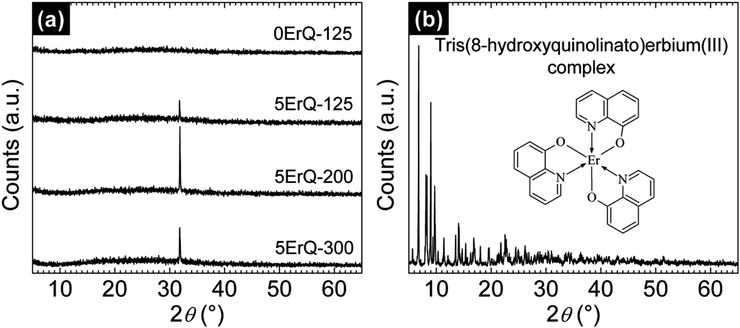
From the structural point of view, the undoped As3S7 thin film was amorphous which was confirmed by the Bragg diffraction pattern in Fig. 3(a). However, the sharp diffraction peak at 2θ ≈ 31.83° was observed for ErQ-doped As3S7 thin films (Fig. 3(a)), which manifests their partially crystalline state. This peak cannot simply be assigned to the ErQ structure since there is no obvious diffraction peak in the powder X-ray diffractogram of pure ErQ presented in Fig. 3(b). The position of the diffraction peak could correspond to some of the S–Er–O miscellaneous compounds such as Er2S2O61 and Er2O2S62 or the ErAs cubic (Fm![[3 with combining macron]](https://www.rsc.org/images/entities/char_0033_0304.gif) m) phase,63 all suggesting that the reaction of ErQ with the As–S glass occurs in a PA environment. It is fair to stress that when ErQ was fully dissolved in the As3S7–PA solution, yellow precipitates appeared after ca. ∼1 h as a consequence of the chemical reaction of both components. Therefore, we can assume that the yellow precipitates can be connected to the separation of the 8-hydroxyquinoline ligands and to the reaction of the Er-based compound in the As3S7–PA environment. We observed that the precipitation is accelerated at higher temperatures or in an ultrasonication bath. Thus, the solutions were immediately filtered, spin-coated and annealed at 125 °C prior to the observation of the precipitates.
m) phase,63 all suggesting that the reaction of ErQ with the As–S glass occurs in a PA environment. It is fair to stress that when ErQ was fully dissolved in the As3S7–PA solution, yellow precipitates appeared after ca. ∼1 h as a consequence of the chemical reaction of both components. Therefore, we can assume that the yellow precipitates can be connected to the separation of the 8-hydroxyquinoline ligands and to the reaction of the Er-based compound in the As3S7–PA environment. We observed that the precipitation is accelerated at higher temperatures or in an ultrasonication bath. Thus, the solutions were immediately filtered, spin-coated and annealed at 125 °C prior to the observation of the precipitates.
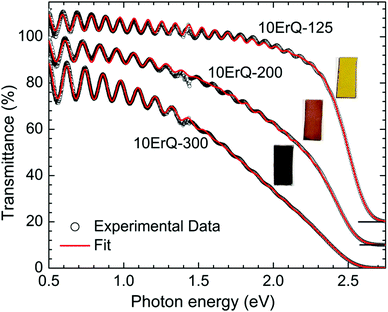
Typical transmittance spectra of the As3S7:ErQ films annealed at various temperatures are shown in Fig. 4 for 10ErQ films. Spectra were fitted using eqn (2)–(5) from which the refractive index n0, optical band gap energy Eg (eV) at α = 103 cm−1 and scattering parameter r (cm−1 eV−4) were calculated and are presented in Table 3. The transmittance spectra of the undoped As3S7 films annealed at 200 °C or 300 °C were not analyzed due to their insufficient optical quality as was observed under an optical microscope, which is previously shown in Fig. 2.
| Sample | 0ErQ-125 | 5ErQ-125 | 5ErQ-200 | 5ErQ-300 | 10ErQ-125 | 10ErQ-200 | 10ErQ-300 |
|---|---|---|---|---|---|---|---|
| n 0 | 2.15 | 1.87 | 1.89 | 2.23 | 1.82 | 1.91 | 2.05 |
| r (cm−1 eV−4) | 29 | 16 | 33 | 217 | 13 | 108 | 217 |
| E g (eV) | 2.36 | 2.42 | 2.38 | 2.35 | 2.43 | 2.37 | 2.34 |
Refractive index n0 increases (Table 3 and Fig. 5) and the absorption edge is red shifted with increasing annealing temperature. This trend is in good agreement with the aforementioned assumption that the annealing process densifies the As3S7:ErQ films due to the evaporation of the residual PA solvent along with a few sulfur-based volatile compounds and Q ligands. The slow increase in the transmittance of samples (∼2.5–1.5 eV) annealed at 300 °C compared to those annealed at 125 °C (Fig. 4) indicates the presence of light scattering. This is supported by the observed increase in the scattering parameter r with annealing temperature in Table 3. The origin of the scattering centres can be assigned to the presence of crystallites (Fig. 3) and/or to the void formation during the PA and H2S evaporation.21 On the other hand, the addition of ErQ to As3S7 decreases the refractive index n0 and increases the optical band gap energy Eg (Table 3 and Fig. 5). This is due to the incorporation of larger and lighter molecules of organic Q ligands (in ErQ) into heavier As3S7 which reduces the optical density of the films.
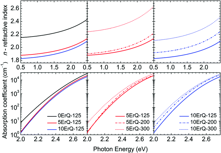 | ||
| Fig. 5 Refractive indices and absorption coefficients of the 0ErQ-125 and As3S7:ErQ films annealed at various temperatures. | ||
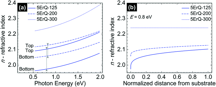
The spectroscopic ellipsometry revealed that the As3S7:ErQ films are transversally graded in the refractive index after annealing at 125 or 200 °C which is shown in Fig. 6 in the case of 5ErQ films. However, the gradation in the refractive index gradually disappears with increasing annealing temperature (Fig. 6) and completely disappears when samples are annealed at 300 °C which is above the softening temperature of the As3S7 glass. At the same time, the refractive index increases with increasing annealing temperature which is given by the densification of the films upon thermal treatment. The transversal gradation of the refractive index can be attributed to the decreasing content of PA from the bottom to the top part of the films. The increasing refractive index from the bottom to the top part of the films shown in Fig. 6(b) suggests that the PA solvent is predominantly evaporated from the top part of the films leading to the densification of this top sublayer. Subsequently, the densified surface can act as a diffusion barrier for further evaporation of PA embedded inside of the films. As already mentioned, even post-annealing of samples at 300 °C does not provide PA-free films.
The Er3+:4I13/2 → 4I15/2 (≈1.5 μm) photoluminescence emission spectra of all the ErQ-doped As3S7 films under 980 nm laser excitation are presented in Fig. 7. The ≈1.5 μm PL intensity is very weak in the case of samples annealed at 125 °C but increases significantly with the annealing temperature and the content of ErQ. It was reported that the ≈1.5 μm PL emission was not observed at a pumping wavelength of 980 nm in hybrid films of organic oxysilanes doped with ErQ in ref. 64 which was ascribed to the low concentration of active Er3+-based PL centres. We assume that the ≈1.5 μm PL emission is not observed in moderately annealed samples due to the presence of the Q ligands (and partially due to the PA content) around Er3+ which can quench the population of the Er3+:4I13/2 level via the multiphonon relaxation such as by the vibrational quanta of the O–H,65 N–H21,22 or C–H21,22,66 groups.
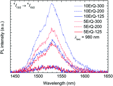 | ||
| Fig. 7 Er3+ ≈1.5 μm PL emission spectra of the As3S7:ErQ films excited with 980 nm laser and annealed at various temperatures. | ||
Moreover, as was mentioned above the Er3+ ≈1.5 μm PL emission band interferes with the strong PA absorption, therefore it is crucial to reduce the PA content to the lowest possible level. Since the content of the nitrogen atoms is very similar in samples annealed at 200 or 300 °C, we can suppose that the increase of the PL emission intensity can be ascribed to the formation of the new PL active centres around Er3+. These centres can originate from the decomposition of the Q ligands around Er3+ and the subsequent evolution of the new O–Er–S or Er–As bonds which suppress more effectively the multiphonon relaxation.
The ≈1.5 μm PL emission recorded for As3S7:ErQ films was successfully observed as well at a pumping wavelength of 808 nm which is the other common diode-laser source. These normalized spectra are compared in Fig. 8 to those monitored at an excitation wavelength of 980 nm. The full width at half maximum (FWHM) of the ≈1.5 μm PL emission is ≈60 nm which is higher than in Er3+-the implanted As–S films67 (FWHM ≈ 45 nm) and lower than in the ErQ films44 (FWHM ≈ 76 nm). Moreover, it seems that the ≈1.5 μm PL emission spectra of the 300 °C post-annealed sample compared to the sample that is post-annealed at 200 °C are slightly shifted to longer wavelengths. This can be related to the reduction of the absorption at this spectral region due to the decomposition of the ErQ complex and possibly to the changes in the Stark splitting due to the increasing effective crystal field around Er ions.68 In other words, the Er3+ local environment is changed and the new optically active centres promoting the ≈1.5 μm PL emission are created.
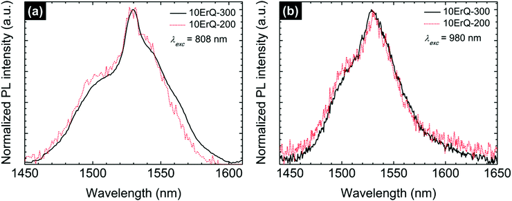 | ||
| Fig. 8 Normalized Er3+ ≈1.5 μm PL emission spectra of the 10ErQ-200 and 10ErQ-300 films excited with (a) 808 nm and (b) 980 nm laser. | ||
The present study shows that the highest PL intensity is achieved for the sample 10ErQ-300, i.e. annealed at 300 °C and doped with ∼10 mol% of ErQ (Fig. 7). Such an ErQ concentration corresponds to ≈1 at% of Er which is beyond the Er solubility limit for the melt-quenched As2S3 glass (∼0.1 at%).44 However, this statement is valid only if all the Er centres are assumed to be PL active which may not be true in real cases such as due to incomplete full ionization of all Er atoms to Er3+ or incomplete decomposition of Q ligands around Er. Anyway, the present approach of two step dissolution of ChGs (As3S7) together with organolanthanide precursors (ErQ) promises the possibility of introducing a significantly higher content of RE3+ ions into chalcogenide films over the solubility limit for bulk glasses which is desired in many applications.
Conclusions
We have successfully spin-coated the As3S7:Er3+ thin films using a two-step solution-based process by (1) dissolving the As3S7 chalcogenide glass with propylamine (PA) and (2) further adding the tris(8-hydroquinoline)erbium(III) complex (ErQ) as an Er3+ precursor. The As3S7:ErQ films were deposited using the spin-coating technique. Spin-coated films were subsequently thermally stabilized at 125 °C and post-annealed at 200 or 300 °C. It was revealed that the presence of ErQ in As3S7 improves the resistance of the films against thermal treatment. Films annealed at temperatures of 125 and 200 °C were graded in the refractive index, however, their post-annealing at 300 °C resulted in homogeneous ungraded films. The gradation in the refractive index was assigned to the transversal distribution of the PA solvent through the As3S7:ErQ films. Even annealing at 300 °C did not lead to the PA-free films which significantly reduces the Er3+:4I13/2 → 4I15/2 (≈1.5 μm) photoluminescence (PL) emission because of the strong PA absorption in this spectral region. Moreover, the presence of Q ligands (from ErQ) may quench the population of the 4I13/2 level via multiphonon relaxation. Thus, negligible ≈1.5 μm PL emission was observed in samples annealed at 125 °C. However, the Er3+ ≈1.5 μm PL emission is promoted with increasing annealing temperature with the most intense PL emission achieved for the As3S7 films annealed at 300 °C, and doped with ≈1 at% of Er. This was attributed not only to the reduction of the PA content in films but also to the appearance of new PL active centres around Er3+ as a consequence of the decomposition of the Q ligands. The Er3+ doping concentration of ≈1 at% in the As3S7:ErQ spin-coated films exceeds the solubility limit in As–S melt-quenched glasses. However, the reduction of the PA solvent from the films remains a crucial issue for PL applications, which can be overcome by using other more volatile or less chemically bonded solvents. The searching for the other combinations of highly transparent chalcogenide host matrixes and decomposable organolanthanide complexes could be beneficial as well. Nevertheless, the solution-processed rare-earth-doped chalcogenide films utilizing the organolanthanide precursors are promising candidates for low-cost and low-temperature production of efficient PL materials in photonics and optoelectronics.Conflicts of interest
There are no conflicts of interest to declare.Acknowledgements
Authors gratefully acknowledge the financial support from the Czech Science Foundation, project No. 15-07912S. Present work was supported by the project CZ.1.05/4.1.00/11.0251 and by project LM2015082 from Center of Materials and Nanotechnologies from the Czech Ministry of Education, Youth and Sports of the Czech Republic. Karel Palka acknowledges the financial support from the Czech Science Foundation, project No. 16-13876S.References
- Y. Ohishi, A. Mori, T. Kanamori, K. Fujiura and S. Sudo, Appl. Phys. Lett., 1994, 65, 13–15 CrossRef CAS.
- C. Koughia, M. G. Brik, G. Soundararajan and S. Kasap, J. Non-Cryst. Solids, 2013, 377, 90–94 CrossRef CAS.
- M. De Sario, L. Mescia, F. Prudenzano, F. Smektala, F. Deseveday, V. Nazabal, J. Troles and L. Brilland, Opt. Laser Technol., 2009, 41, 99–106 CrossRef CAS.
- J. A. Frantz, L. B. Shaw, J. S. Sanghera and I. D. Aggarwal, Opt. Express, 2006, 14, 1797–1803 CrossRef CAS PubMed.
- M. R. E. Lamont, B. Luther-Davies, D. Y. Choi, S. Madden and B. J. Eggleton, Opt. Express, 2008, 16, 14938–14944 CrossRef CAS PubMed.
- J. S. Sanghera and I. D. Aggarwal, J. Non-Cryst. Solids, 1999, 256, 6–16 CrossRef.
- F. Starecki, F. Charpentier, J. L. Doualan, L. Quetel, K. Michel, R. Chahal, J. Troles, B. Bureau, A. Braud, P. Camy, V. Moizan and V. Nazabal, Sens. Actuators, B, 2015, 207, 518–525 CrossRef CAS.
- A. L. Pelé, A. Braud, J. L. Doualan, R. Chahal, V. Nazabal, C. Boussard-Plédel, B. Bureau, R. Moncorgé and P. Camy, Opt. Express, 2015, 23, 4163–4172 CrossRef PubMed.
- J. Planelles-Aragó, B. Julián-López, E. Cordoncillo, P. Escribano, F. Pellé, B. Viana and C. Sanchez, J. Mater. Chem., 2008, 18, 5193–5199 RSC.
- P. F. Smet, I. Moreels, Z. Hens and D. Poelman, Materials, 2010, 3, 2834–2883 CrossRef CAS.
- J. F. Suijver, Luminescence: From theory to applications, Wiley-VCH Verlag GmbH & Co. KGaA, Weinheim, 2008, ch. 6, Upconversion phosphors, pp. 133–177 Search PubMed.
- C. Chen, X. He, L. Gao and N. Ma, ACS Appl. Mater. Interfaces, 2013, 5, 1149–1155 CAS.
- A. Zakery and S. R. Elliott, J. Non-Cryst. Solids, 2003, 330, 1–12 CrossRef CAS.
- N. F. Mott and E. A. Davis, Electronic processes in non-crystalline materials, Clarendon Press, Oxford University Press, Oxford, 1979 Search PubMed.
- K. Tanaka and K. Shimakawa, Amorphous chalcogenide semiconductors and related materials, Springer, New York, 2011 Search PubMed.
- S. Kasap, K. Koughia, G. Soundararajan and M. G. Brik, IEEE J. Sel. Top. Quantum Electron., 2008, 14, 1353–1360 CrossRef CAS.
- S. O. Kasap, K. Koughia, M. Munzar, D. Tonchev, D. Saitou and T. Aoki, J. Non-Cryst. Solids, 2007, 353, 1364–1371 CrossRef CAS.
- J. Orava, T. Kohoutek and T. Wagner, Deposition techniques for chalcogenide thin films, in Chalcogenide glasses: Preparation, properties and applications, ed. J.-L. Adam and X. Zhang, Woodhead Publishing, Daryaganj, 2014, ch. 9, pp. 265–309 Search PubMed.
- D. B. Mitzi, J. Mater. Chem., 2004, 14, 2355–2365 RSC.
- M. Yuan and D. B. Mitzi, Dalton Trans., 2009, 6078–6088 RSC.
- S. Song, J. Dua and C. B. Arnold, Opt. Express, 2010, 18, 5472–5480 CrossRef CAS PubMed.
- Y. Zou, H. Lin, O. Ogbuu, L. Li, S. Danto, S. Novak, J. Novak, J. D. Musgraves, K. Richardson and J. Hu, Opt. Mater. Express, 2012, 2, 1723–1732 CrossRef CAS.
- S. Slang, P. Janicek, K. Palka and M. Vlcek, Opt. Mater. Express, 2016, 6, 1973–1985 CrossRef CAS.
- M. Waldmann, J. D. Musgraves, K. Richardson and C. B. Arnold, J. Mater. Chem., 2012, 22, 17848–17852 RSC.
- M. Yuan, D. B. Mitzi, W. Liu, A. J. Kellock, S. J. Chey and V. R. Deline, Chem. Mater., 2010, 22, 285–287 CrossRef CAS.
- D. J. Milliron, D. B. Mitzi, M. Copel and C. E. Murray, Chem. Mater., 2006, 18(3), 587–590 CrossRef CAS.
- Y. Ma, M. Liu, A. Jaber and R. Y. Wang, J. Mater. Chem. A, 2015, 3, 13483–13491 CAS.
- D. B. Mitzi, L. L. Kosbar, C. E. Murray, M. Copel and A. Afzali, Nature, 2004, 428, 299–303 CrossRef CAS PubMed.
- D. B. Mitzi, M. Copel and S. J. Chey, Adv. Mater., 2005, 17, 1285–1289 CrossRef CAS.
- W. Liu, D. B. Mitzi, M. Yuan, A. J. Kellock, S. Jay Chey and O. Gunawan, Chem. Mater., 2010, 22, 1010–1014 CrossRef CAS.
- J. B. Seon, S. Lee, J. M. Kim and H. D. Jeong, Chem. Mater., 2009, 21, 604–611 CrossRef CAS.
- T. Todorov and D. B. Mitzi, Eur. J. Inorg. Chem., 2010, 17–28 CrossRef CAS.
- R. Y. Wang, J. P. Feser, X. Gu, K. M. Yu, R. A. Segalman, A. Majumdar, D. J. Milliron and J. J. Urban, Chem. Mater., 2010, 22, 1943–1945 CrossRef CAS.
- R. Zhang, S. M. Szczepaniak, N. J. Carter, C. A. Handwerker and R. Agrawal, Chem. Mater., 2015, 27, 2114–2120 CrossRef CAS.
- T. Kohoutek, J. Orava, T. Sawada and H. Fudouzi, J. Colloid Interface Sci., 2011, 353, 454–458 CrossRef CAS PubMed.
- D. B. Mitzi, S. Raoux, A. G. Schrott, M. Copel, A. Kellock and J. Jordan-Sweet, Chem. Mater., 2006, 18, 6278–6282 CrossRef CAS.
- D. B. Mitzi, Adv. Mater., 2009, 21, 3141–3158 CrossRef CAS.
- D. H. Webber and R. L. Brutchey, J. Am. Chem. Soc., 2013, 135, 15722–15725 CrossRef CAS PubMed.
- T. H. Lee, S. I. Simdyankin, J. Hegedus, J. Heo and S. R. Elliott, Phys. Rev. B: Condens. Matter Mater. Phys., 2010, 81, 104204 CrossRef.
- J. Heo, J. Mater. Sci. Lett., 1995, 14, 1014–1016 CrossRef CAS.
- J. Ikuta, K. Maeda, T. Sakai, T. Ikari, K. Koughia, M. Munzar and S. O. Kasap, J. Mater. Sci.: Mater. Electron., 2007, 18, 231–234 CrossRef.
- S. Das and K. C. Mandal, Mater. Lett., 2012, 66, 46–49 CrossRef CAS.
- S. Tanabe and T. Hanada, J. Non-Cryst. Solids, 1996, 196, 101–105 CrossRef CAS.
- R. J. Curry and W. P. Gillin, Appl. Phys. Lett., 1999, 75, 1380–1382 CrossRef CAS.
- W. Q. Zhao, G. Z. Ran, G. L. Ma, W. J. Xu, L. Dai, W. M. Liu, P. F. Wang and G. G. Qin, Appl. Phys. Lett., 2006, 89, 022109 CrossRef.
- J. Thompson, R. I. R. Blyth, G. Gigli and R. Cingolani, Adv. Funct. Mater., 2004, 14, 979–984 CrossRef CAS.
- R. J. Curry and W. P. Gillin, Synth. Met., 2000, 111, 35–38 CrossRef.
- W. P. Gillin and R. J. Curry, Appl. Phys. Lett., 1999, 74, 798–799 CrossRef CAS.
- S. Penna, L. Mattiello, S. Di Bartolo, A. Pizzoleo, V. Attanasio, G. M. Tosi Beleffi and A. Otomo, J. Nanosci. Nanotechnol., 2016, 16, 3360–3363 CrossRef CAS PubMed.
- R. Swanepoel, J. Phys. E: Sci. Instrum., 1983, 16, 1214–1222 CrossRef CAS.
- R. Swanepoel, J. Phys. E: Sci. Instrum., 1984, 17, 896–903 CrossRef CAS.
- S. Kasap and P. Capper, Swanepoel's analysis of optical transmission spectra, Springer handbook of electronic and photonic materials, Springer, New York, 2006, ch. 3.4.1, pp. 71–72 Search PubMed.
- W. Sellmeier, Ann. Phys. Chem., 1871, 219, 272–282 CrossRef.
- L. Rayleigh, Philos. Mag., 1892, 34, 481–502 CrossRef.
- L. Cauchy, Bull. Sci. Math., 1830, 14, 9 Search PubMed.
- J. Orava, J. Šik, T. Wágner and M. Frumar, J. Appl. Phys., 2008, 103, 083512 CrossRef.
- D. A. G. Bruggeman, Ann. Phys., 1935, 416, 636–664 CrossRef.
- T. Kohoutek, T. Wagner, M. Frumar, A. Chrissanthopoulos, O. Kostadinova and S. N. Yannopoulos, J. Appl. Phys., 2008, 103, 063511 CrossRef.
- T. Kohoutek, J. Orava, L. Strizik, T. Wagner, A. L. Greer, M. Bardosova and H. Fudouzi, Opt. Mater., 2013, 36, 390–395 CrossRef CAS.
- S. Penna, PhD thesis, University of Rome Tor Vergata, 2009.
- K. J. Range, K. G. Lange and A. Gietl, J. Less-Common Met., 1990, 158, 137–145 CrossRef CAS.
- W. Sun, H. Xu, X. Qiu, M. Yu, L. Wang and Q. Zhang, J. Mater. Sci.: Mater. Electron., 2016, 27, 11049–11054 CrossRef CAS.
- H. E. Swanson, M. C. Morris and E. H. Evans, Erbium Arsenide, ErAs, Standard X-ray diffraction powder patterns: Section 4, U.S. Dpt. of Commerce, National Bureau of Standards, Washington D.C., 1966, p. 54 Search PubMed.
- O. H. Park, S. Y. Seo, B. S. Bae and J. H. Shin, Appl. Phys. Lett., 2003, 82, 2787–2789 CrossRef CAS.
- V. Krishnakumar and R. Ramasamy, Spectrochim. Acta, Part A, 2005, 61, 673–683 CrossRef CAS PubMed.
- L. Winkless, R. H. C. Tan, Y. Zheng, M. Motevalli, P. B. Wyatt and W. P. Gillin, Appl. Phys. Lett., 2006, 89, 111115 CrossRef.
- J. Fick, É. J. Knystautas, A. Villeneuve, F. Schiettekatte, S. Roorda and K. A. Richardson, J. Non-Cryst. Solids, 2000, 272, 200–208 CrossRef CAS.
- Z. G. Ivanova, K. Koughia, Z. Aneva, D. Tonchev, V. S. Vassilev and S. O. Kasap, J. Optoelectron. Adv. Mater., 2005, 7, 349–352 CAS.
Footnote |
| † Corresponding authors contributed equally to the present work. |
| This journal is © The Royal Society of Chemistry 2017 |

