
Directly writing 2D organic semiconducting crystals for high-performance field-effect transistors†
Yujia
Zhang
,
Yu
Guo
,
Lei
Song
,
Jun
Qian
,
Sai
Jiang
,
Qijing
Wang
,
Xinran
Wang
,
Yi
Shi
*,
Xiaomu
Wang
 * and
Yun
Li
*
* and
Yun
Li
*
National Laboratory of Solid State Microstructures, School of Electronic Science and Engineering, Collaborative Innovation Center of Advanced Microstructures, Nanjing University, Nanjing 210093, P. R. China. E-mail: yli@nju.edu.cn; xiaomu.wang@nju.edu.cn; yshi@nju.edu.cn
First published on 4th July 2017
Abstract
Solution-processed 2D organic crystals are of significant interest because of their unique characteristics that ensure promising applications in electronics. In this study, a simple and efficient approach to directly write 2D organic crystals using a rollerball pen has been presented. The obtained crystals exhibit highly crystalline features with atomic smoothness and large size. Field-effect transistors composed of the obtained crystals yield an average and a maximum carrier mobility values of 3.1 and 5.9 cm2 V−1 s−1, respectively. This study presents significant potential of the writing technique via a rollerball pen for the solution-processed fabrication of 2D organic crystals for high-performance, large-area printed electronics.
Introduction
Two-dimensional (2D) crystalline organic semiconductors, which are defined as few-layered structures with conjugated molecules well-packed by van der Waals interactions, are of significant interest as a promising class of materials for electronic applications.1–19 Field-effect transistors (FETs) with the carrier mobility values of over 10 cm2 V−1 s−1 have been well demonstrated using 2D organic semiconducting crystals.1,2 These high carrier mobility values are attributed to their high packing orders and remarkable direct charge injection because of their ultrathin thickness. To date, intensive efforts have been devoted to solution-based techniques, such as spin-coating and drop-casting, for the deposition of 2D semiconducting organic crystals; these techniques allow the low-cost and high-throughput manufacturing of electronic devices.1,3–9 Recently, we have presented an antisolvent-crystallization-assisted approach, which constitutes a floating-coffee-ring-driven assembly, for the fabrication of 2D organic crystals with atomic smoothness and high film uniformity over a large area for applications such as in high-performance organic field-effect transistors (OFETs).1 To further advance 2D organic crystals toward printed electronics, development of a solution-coating method using a facile tool for the rapid and deposition-at-will fabrication is critical.20 In our previous research, it has been shown that a rollerball pen, which is a daily-used writing instrument, is promising for this deposition process, and its flow behaviour intrinsically facilitates the formation of high-quality and large-area organic bulk crystals.21 Therefore, directly writing 2D crystalline organic semiconductors using the combination of antisolvent crystallization and flow behaviour from a rollerball pen is greatly interesting.In this study, we demonstrated a novel strategy for the fabrication of solution-processed 2D organic semiconductors using a commercially available rollerball pen. The deposited 2D films exhibit highly crystalline features with an atomic smoothness over a large area of >450 μm. Bottom-gate top-contact FETs yield an average and a maximum carrier mobility value of 3.1 and 5.9 cm2 V−1 s−1, respectively. Our results confirm that the writing technique using a rollerball pen is simple yet promising for the fabrication of 2D organic crystals for high-performance and large-area printed electronics.
Experimental
2D organic semiconducting crystals written by a rollerball pen
The small-molecule semiconductor dioctylbenzothienobenzothiophene (C8-BTBT) was purchased from Nippon Kayaku Co. C8-BTBT was dissolved in anisole (Sigma-Aldrich), and a small amount of p-anisaldehyde (0.5 wt%) was added as the antisolvent. A commercial rollerball pen (Pelikan rollerball pen refill 338F) was used for the deposition of the organic crystals because it was mainly made of metal. The non-metallic rear cap of the refill was removed, and the ink was carefully cleaned. The abovementioned solution (∼40 μL) was injected into the refill tube. The deposition of 2D organic crystals was performed via the hand-writing process at a steady speed. The hydrophilicity of the SiO2/Si substrate was enhanced through UV-ozone treatment (Fig. S1, ESI†), and a fine-sized nib allowed the examination of the minimum width of the written line. The pen nib gently touched the pre-cleaned SiO2/Si substrate surface to avoid scratching of the SiO2 surface, with a writing speed of ∼1 mm s−1 under ambient conditions at room temperature, for the deposition of 2D organic semiconducting crystals. We measured the length of the written stripe consisting of 2D organic crystals. Further, the writing speed was estimated by dividing the stripe length by the time taken to perform the deposition.Characterizations of the 2D organic crystals
Optical microscopic images were obtained using a Keyence VHX-5000 digital microscope (VHX-S550E). The colours of the figures for 2D organic crystals were modified for improved visibility. For regular atomic force microscopy (AFM) measurements, a Veeco Multimode 8 was used under ambient conditions. For high-resolution AFM, an Asylum Cypher was used under ambient conditions using Asylum ARROW UHF AFM tips.Fabrication and electrical measurements of FETs
For the fabrication of the transistor devices, Au pads (30 μm × 100 μm) were thermally evaporated at a deposition rate of 0.2 Å s−1 to reach a thickness of 100 nm. Then, the Au pads were transferred onto the top of the 2D C8-BTBT crystals by the stamping method to form the source and drain electrodes. The electrical characteristics of the fabricated FETs were measured using an Agilent B1500 semiconductor parameter analyser in a closed-cycle cryogenic probe station with a base pressure of 10−5 Torr.Results and discussion
The p-type small molecule C8-BTBT was selected because of its high carrier mobility and good solubility.22–24 The highest occupied molecular orbital (HOMO) and the lowest unoccupied molecular orbital (LUMO) of C8-BTBT are −5.4 and −1.6 eV, respectively.25 C8-BTBT molecules were dissolved in a mixture solvent containing a good solvent of anisole and a small amount of p-anisaldehyde as the antisolvent (0.5 wt%). Fig. 1a and b show the optical images of the rollerball pen refill and the metal ball at the nib, respectively. Pressurized ink was constantly pressed against the interior side of the ball, and the ink was released by the capillary effect at the narrow aperture around the metal ball onto the substrate. As shown in Fig. 1c, the appropriate writing speed generated a thin solution edge, at which a high evaporation rate was achieved. Thus, the evaporation-driven flow led to a floating-coffee-ring effect near the solution edge, serving as an ideal location for the formation of ultrathin 2D C8-BTBT crystals.1 | ||
| Fig. 1 (a) Optical image of the rollerball pen refill tube. (b) Optical microscopy image of the rollerball pen nib. (c) Schematic of the deposition of 2D organic crystals written by a rollerball pen. Ellipsoids represent C8-BTBT molecules. | ||
The inset of Fig. 2a shows the optical microscopy image of a curved line with a width of ∼830 μm written with the rollerball pen. The line consists of ultrathin C8-BTBT crystals with 2D material features, precise layer definition, and large area typically of ∼450 μm (Fig. 2a). Moreover, we further studied the morphological properties of the crystals via AFM characterization. Fig. 2b and c show the AFM images of the two steps, as marked by the dotted squares in Fig. 2a, where the thicknesses are 5.4 and 3.0 nm, respectively. The molecules in the third layer were almost perpendicular to the substrates because the molecular length of C8-BTBT was ∼3.0 nm.26,27 Our previous results showed that the C8-BTBT molecules in the first layer were more tilted to the substrate than that in the upper layers because the van der Waals interactions among the molecules decreased rapidly from the C8-BTBT/SiO2 surface to the upper molecular layers.1,2 Furthermore, both the bi- and tri-layer C8-BTBTs exhibited uniform thin films with atomic smoothness, and the root-mean-square roughness was 1.2 and 1.3 Å for the second and third molecules, respectively. These smooth surfaces and the step-and-terrace structure indicate the highly crystalline features of the molecular crystals written with the rollerball pen.23,28
 | ||
| Fig. 2 (a) Optical microscopy image of a 2D C8-BTBT crystalline film mainly consisting of bi- and tri-layer molecules. The layer-by-layer manner dominates the growth of 2D organic crystals. Inset shows a curved line written by a rollerball pen. Scale bar is 200 μm. This line consists of ultrathin C8-BTBT crystals with 2D material features. (b and c) AFM morphological images of bi- and tri-layer C8-BTBT, respectively. The height profiles correspond to the white dotted lines in the AFM images. Scale bars are 1 μm. (d and e) High-resolution AFM images of bi- and tri-layer C8-BTBT molecules, respectively. Insets are the corresponding fast Fourier transforms of the AFM images with lattice indices. Scale bars are 1 nm. | ||
The crystalline properties were characterized via the high-resolution AFM measurements. More than six areas were randomly scanned (Fig. S2 and S3, ESI†) for both the bi- and tri-layer films. For the bi-layer film, the AFM images show nearly identical lattice constants of a = 6.41 ± 0.16 Å, b = 8.19 ± 0.12 Å, and θ = 88.6 ± 1.4°. Therefore, the images indicate a single-crystalline phase for the bi-layer film over a large area. Furthermore, similar single crystalline characteristics were observed in the tri-layer C8-BTBT (Fig. 2e and Fig. S2, ESI†). The crystalline properties of the molecular crystals are summarized in Table 1.
| Layer | Height (nm) | RMS roughness (Å) | Lattice constant | ||
|---|---|---|---|---|---|
| a (Å) | b (Å) | θ (°) | |||
| 2L | 3.0 ± 0.1 | 1.2 | 6.41 ± 0.16 | 8.19 ± 0.12 | 88.6 ± 1.4 |
| 3L | 3.0 ± 0.1 | 1.3 | 6.25 ± 0.15 | 8.16 ± 0.12 | 87.2 ± 1.8 |
Subsequently, we changed the p-anisaldehyde concentration to examine the role of the antisolvent in the writing process. As shown in Fig. 3a, the obtained film exhibited a polycrystalline phase when the solution contained no p-anisaldehyde (0 wt%). Furthermore, the brightness of the crystals indicates a bulk-crystal feature with a relatively large thickness. As the antisolvent concentration increased to 0.5 wt%, a uniform film with an ultrathin thickness over a large area of ∼350 μm was observed. This film mainly consisted of bi- and tri-layer molecules (Fig. 3b). When the antisolvent concentration was 1 wt% and 5 wt%, the deposited film also consisted of small and isolated crystals, and the size of the 2D crystals decreased significantly (Fig. 3c and d, respectively). Further increase in the antisolvent concentration to 20 wt% led to the transformation of almost all the C8-BTBT molecules into microcrystals, and 2D organic crystals were hardly observed (Fig. 3e). Thus, the addition of an appropriate amount of antisolvent is critical for the fabrication of 2D organic crystals.
 | ||
| Fig. 3 (a–e) Microscopic images of C8-BTBT films written by a rollerball pen using anisole/p-anisaldehyde mixture solutions with different antisolvent concentrations. Scale bars are all 50 μm. | ||
Furthermore, writing speed is a key parameter for the achievement of 2D organic crystals through the deposition process. The solution was casted from a still rollerball pen when the writing speed was 0 mm s−1. The deposited film exhibited a polycrystalline phase after the solvent was naturally dried, mainly consisting of bulk crystals (Fig. 4a). As shown in Fig. 4b, considerably thinner C8-BTBT film molecules were deposited when the writing speed increased to 0.5 and 1 mm s−1. The optimized speed of 1 mm s−1 resulted in the formation of C8-BTBT films with 2D features of few-layered structures in a large area (Fig. 4c). We observed large bulk crystals at the edge and a non-uniform polycrystalline film in the interior part of the coating area when the writing speed was as high as 10 mm s−1 (Fig. 4d). Therefore, the writing speed, as a critical parameter for the deposition process, has a strong influence on the film morphological properties.
 | ||
| Fig. 4 (a–d) Microscopic images of C8-BTBT films written by a rollerball pen with different writing speeds. Scales are all 50 μm. | ||
The basic characteristics of our writing process are similar to those reported in our previous work.1 Thus, the addition of the antisolvent p-anisaldehyde induced a coffee-ring effect of the good solvent floating on the antisolvent. As illustrated in Fig. 1c, an appropriate writing speed can lead to a thin solution with a limited quantity and a high evaporation rate near the solution edge. The differences in the boiling points and mass density of the good solvent of anisole (154 °C, 0.99 g mL−1) and antisolvent (258 °C, 1.22 g mL−1) induced a floating-coffee-ring effect of anisole on the antisolvent layer near the solution edge.1,29 This location is ideal for the diffusion and self-organization of the C8-BTBT molecules into 2D crystals.1,23 Moreover, on lowering the writing speed, deposition of organic molecules in relatively large amounts was observed; thus, bulk crystals were obtained. Moreover, higher writing speed did not assure sufficient solution suppleness to maintain a continuous flow from the pen nib to the substrate; thus, isolated microcrystals were formed.
To examine the electrical properties of the 2D C8-BTBT crystals, we fabricated planar FETs with a bottom-gate top-contact geometry (Fig. 5a). A stamping method was used for the formation of the Au source and drain electrodes.30Fig. 5b shows the typical transfer characteristics, including the high field-effect carrier mobility (μFET) of 3.3 cm2 V−1 s−1, large on/off ratio of 107, and threshold voltage (Vth) of −6 V. In addition, the low subthreshold swing (SS) of 0.4 V dec−1 indicates a low maximum trap density at the organic/insulator interface.31,32 The output curves exhibited good saturation behaviour at a high-drain voltage, indicating good FET features (Fig. 5c). Negligible hysteresis was observed both in the transfer and output curves. Subsequently, we fabricated and measured more than ten individual OFETs based on our ultrathin C8-BTBT crystals, yielding an average carrier mobility of 3.1 cm2 V−1 s−1. The highest carrier mobility among these OFETs was 5.9 cm2 V−1 s−1 (Fig. S4, ESI†). To the best of our knowledge, our results represent a record-high value for pen-written organic field-effect transistors.33
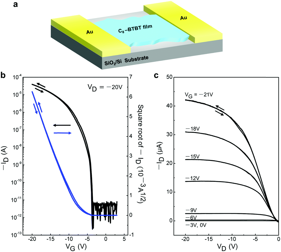 | ||
| Fig. 5 (a) Schematic device structure of the FET using 2D C8-BTBT crystals. (b and c) Transfer and output characteristics of a typical transistor based on written 2D C8-BTBT crystals, respectively. | ||
Furthermore, Fig. 6 shows that a nearly negligible change in the value of μFET is observed in a high-value range of the effective electric field (Eeff), controlling the charge carriers at the channel region. For comparison, we also measured FETs using bulk C8-BTBT crystals fabricated through the same process. A relatively low value of ∼0.1 cm2 V−1 s−1 for the maximum carrier mobility was obtained. Interestingly, a rapid decrease in the carrier mobility with the effective electric field was observed. The carrier mobility can be expressed as follows:34–36
 | (1) |
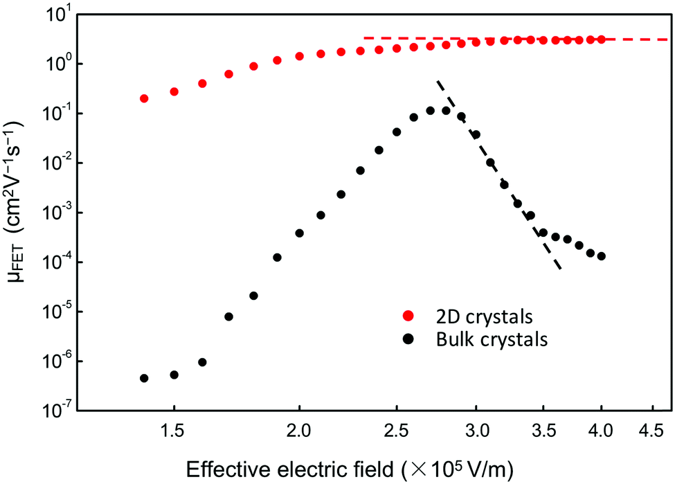 | ||
| Fig. 6 Dependence of μFET of devices using 2D (red circles) and bulk (black squares) C8-BTBT films on Eeff, which controls the charge carriers in the channel regions. | ||
Conclusions
In conclusion, we demonstrated a novel approach for the rapid fabrication of large-area 2D organic semiconducting crystals written directly by a rollerball pen. The deposited 2D crystals exhibit atomic smoothness and large-area uniformity. The resulting OFET devices display good electrical performance, yielding a maximum carrier mobility of 5.9 cm2 V−1 s−1 and high on/off ratio of 107. Our results revealed that the facile writing instrument of a rollerball pen could act as a simple and efficient tool for the fabrication of 2D organic crystals for high-performance printed electronic devices.Acknowledgements
This study was supported partially by 973 projects under Grant No. 2013CBA01600 and 2013CB932900, NSFC under Grant No. 61574074, and Open Partnership Joint Projects of NSFC-JSPS Bilateral Joint Research Projects under Grant No. 61511140098.References
- Q. Wang, J. Qian, Y. Li, Y. Zhang, D. He, S. Jiang, Y. Wang, X. Wang, L. Pan, J. Wang, X. Wang, Z. Hu, H. Nan, Z. Ni, Y. Zheng and Yi Shi, Adv. Funct. Mater., 2016, 26, 3191 CrossRef CAS.
- D. He, Y. Zhang, Q. Wu, R. Xu, H. Nan, J. Liu, J. Yao, Z. Wang, S. Yuan, Y. Li, Y. Shi, J. Wang, Z. Ni, L. He, F. Miao, F. Song, H. Xu, K. Watanaba, T. Taniguchi, J. Xu and X. Wang, Nat. Commun., 2014, 5, 1 Search PubMed.
- J. Huang, J. Sun and H. E. Katz, Adv. Mater., 2008, 20, 2567 CrossRef CAS.
- E. M. Mannebach, J. W. Spalenka, P. S. Johnson, Z. Cai, F. J. Himpsel and P. G. Evans, Adv. Funct. Mater., 2012, 23, 554 CrossRef.
- B.-N. Park, S. Seo and P. G. Evans, J. Phys. D: Appl. Phys., 2007, 40, 3506 CrossRef CAS.
- K. Asadi, Y. Wu, F. Gholamrezaie, P. Rudolf and P. W. M. Blom, Adv. Mater., 2009, 21, 4109 CrossRef CAS.
- H. Chen, S. Dong, M. Bai, N. Cheng, H. Wang, M. Li, H. Du, S. Hu, Y. Yang, T. Yang, F. Zhang, L. Gu, S. Meng, S. Hou and X. Guo, Adv. Mater., 2015, 27, 2113 CrossRef CAS PubMed.
- M. Defaux, F. Gholamrezaie and J. Wang, Adv. Funct. Mater., 2012, 24, 973 CrossRef CAS PubMed.
- D. O. Hutchins, O. Acton, T. Weidner, N. Cernetic, J. E. Baio, G. Ting, D. G. Castner, H. Ma and A. K.-Y. Jen, Org. Electron., 2012, 13, 464 CrossRef CAS.
- L. Shan, D. Liu, H. Li, X. Xu, B. Shan, J.-B. Xu and Q. Miao, Adv. Mater., 2015, 27, 3418 CrossRef CAS PubMed.
- B. Wang, T. Zhu, L. Huang, T. L. D. Tam, Z. Cui, J. Ding and L. Chi, Org. Electron., 2015, 24, 170 CrossRef CAS.
- L. Li, P. Gao, W. Wang, K. Müllen, H. Fuchs and L. Chi, Angew. Chem., Int. Ed., 2013, 52, 12530 CrossRef CAS PubMed.
- L. Li, P. Gao, K. C. Schuermann, S. Ostendorp, W. Wang, C. Du, Y. Lei, H. Fuchs, L. D. Cola, K. Müllen and L. Chi, J. Am. Chem. Soc., 2010, 132, 8807 CrossRef CAS PubMed.
- L. Jiang, H. Dong, Q. Meng, H. Li, M. He, Z. Wei, Y. He and W. Hu, Adv. Mater., 2011, 23, 2059 CrossRef CAS PubMed.
- S. Mathijssen, E. Smits and P. A. van Hal, Nat. Nanotechnol., 2009, 4, 674 CrossRef CAS PubMed.
- S. A. DiBenedetto, A. Facchetti, M. A. Ratner and T. J. Marks, Adv. Mater., 2009, 21, 1407 CrossRef CAS.
- M. Mottaghi, P. Lang, F. Rodriguez, A. Rumyantseva, A. Yassar, G. Horowitz, S. Lenfant, D. Tondelier and D. Vuillaume, Adv. Funct. Mater., 2007, 17, 597 CrossRef CAS.
- A. Ringk, W. S. C. Roelofs, E. C. P. Smits, C. van der Marel, I. Salzmann, A. Neuhold, G. H. Gelinck, R. Resel, D. M. de Leeuw and P. Strohriegl, Org. Electron., 2013, 14, 1297 CrossRef CAS.
- L. Song, Y. Wang, Q. Gao, Y. Guo, Q. Wang, J. Qian, S. Jiang, B. Wu, X. Wang, Y. Shi, Y. Zheng and Y. Li, ACS Appl. Mater. Interfaces, 2017, 9, 18127 CAS.
- H. Sun, Q. Wang, J. Qian, Y. Yin, Y. Shi and Y. Li, Semicond. Sci. Technol., 2015, 30, 054001 CrossRef.
- Y. Wang, L. Chen, Q. Wang, H. Sun, X. Wang, Z. Hu, Y. Shi and Y. Li, Org. Electron., 2014, 15, 2234 CrossRef CAS.
- H. Ebata, T. Izawa, E. Miyazaki, K. Takimiya, M. Ikeda, H. Kuwabara and T. Yui, J. Am. Chem. Soc., 2007, 129, 15732 CrossRef CAS PubMed.
- H. Minemawari, T. Yamada, H. Matsui, J. Tsutsumi, S. Haas, R. Chiba, R. Kumai and T. Hasegawa, Nature, 2012, 475, 364 CrossRef PubMed.
- Y. Yuan, G. Giri, A. L. Ayzner, A. P. Zoombelt, S. C. B. Mannsfeld, J. Chen, D. Nordlund, M. F. Toney, J. Huang and Z. Bao, Nat. Commun., 2014, 5, 3005 Search PubMed.
- H. Kobayashi., N. Kobayashi, S. Hosoi, D. Murakami, R. Shirasawa, Y. Kudo, D. Hobara, Y. Tokita and M. Itabashi, J. Chem. Phys., 2013, 139, 014707 CrossRef PubMed.
- T. Minari, M. Kano, T. Miyadera, S. Wang, Y. Aoyagi, M. Seto, T. Nemoto, S. Isoda and T. Tsukagoshi, Appl. Phys. Lett., 2008, 92, 173301 CrossRef.
- T. Uemura, Y. Hirose, M. Uno, K. Takimiya and J. Takeya, Appl. Phys. Express, 2009, 2, 111501 CrossRef.
- C. Liu, Y. Li, Y. Xu, T. Minari, S. Li, K. Takimiya and K. Tsukagoshi, Org. Electron., 2009, 13, 2975 CrossRef.
- R. D. Deegan, O. Bakajin, T. F. Dupont, G. Huber, S. R. Nagel and T. A. Witten, Nature, 1997, 389, 827 CrossRef CAS.
- Q. Tang, Y. Tong, H. Li, Z. Ji, L. Li, W. Hu, Y. Liu and D. Zhu, Adv. Mater., 2008, 20, 1511 CrossRef CAS.
- S. H. Kim, D. Choi, D. S. Chung, C. Yang, J. Jang, C. E. Park and S. K. Park, Appl. Phys. Lett., 2008, 93, 113306 CrossRef.
- M. McDowell, I. G. Hill, J. E. McDermott, S. L. Nernasek and J. Schwartz, Appl. Phys. Lett., 2006, 88, 073505 CrossRef.
- Z. Li, H. Liu, C. Ouyang, W. H. Wee, X. Cui, T. J. Lu, B. Pingguan-Murphy, F. Li and F. Xu, Adv. Funct. Mater., 2016, 26, 165 CrossRef CAS.
- H. Sun, Q. Wang, Y. Li, Y. Lin, Y. Wang, Y. Yin, Y. Xu, C. Liu, K. Tsukagoshi, L. Pan, X. Wang, Z. Hu and Y. Shi, Sci. Rep., 2014, 4, 7227 CrossRef CAS PubMed.
- S. I. Takagi, T. Toriumi, M. Iwase and H. Tango, IEEE Trans. Electron Devices, 1994, 41, 2357 CrossRef CAS.
- S. I. Takagi, T. Toriumi, M. Iwase and H. Tango, IEEE Trans. Electron Devices, 1994, 41, 2363 CrossRef CAS.
Footnote |
| † Electronic supplementary information (ESI) available. See DOI: 10.1039/c7tc02348k |
| This journal is © The Royal Society of Chemistry 2017 |