In situ self-assembly and photopolymerization for hetero-phase synthesis and patterning of conducting materials using soft oxometalates in thermo-optical tweezers†
Received
4th May 2017
, Accepted 12th June 2017
First published on 13th June 2017
Abstract
We demonstrate a novel method of simultaneous photoassisted hetero-phase synthesis, doping, and micro-scale patterning of conductive materials. The patterning is performed by controlled self-assembly mediated by a micro-bubble induced in an optical tweezers configuration. The high temperature generated due to the light field of the tweezers also drives diverse chemical reactions that lead to the in situ formation of conducting metal-oxides and polymers due to a charge transfer mechanism with soft oxometalates (SOMs). We synthesize two conducting polymers – polypyrrole and polyaniline – doped by the metal oxides Mo–O2 and Mo–O3, from dispersions of the respective organic compounds with the SOMs, and form permanent patterns out of them by continuous self-assembly arising from manipulation of the micro-bubble using Marangoni flows generated by the tweezers. The electrically conducting patterns of width varying between around 4–50 μm, are written in the form of simple Hall-bar geometries, and a four-probe measurement technique yields conductivities on the order of ∼450–600 Siemens cm−1 – which is much higher than that reported for both polypyrrole and polyaniline in earlier work. This technique can easily be used in patterning complicated electrical circuits in mesoscopic length scales, and can also be extended to solution processed electronic device development by green chemical routes.
Introduction
Directed self-assembly,1–5 especially in the meso-scale, has generated significant interest in the scientific community due to the degree of control it provides in creating structures of choice.6–8 It has thus facilitated diverse research of a highly interdisciplinary nature with applications extending from nanotechnology to miniaturized electronics.9–11 The latter has especially attracted a lot of attention in recent times with several techniques being proposed, of which solution processed electronics has gained considerable prominence due to the simplicity and flexibility of the process, its low cost, etc.12 Conducting polymers form the basis of most solution processed electronics, and techniques that can synthesize such materials efficiently and quickly are thus of crucial importance. However, the conductivity of such polymers is often limited and is also critically dependent on the synthesis itself so that a wide range of conductivities of the same type of polymer is often observed.13,14 In fact, several of the conducting polymers have inherently low conductivity that, however, can be considerably enhanced by doping.15–17 The doping process is typically separate from the basic polymer synthesis and is often rather complicated.15 Thus, it would be extremely useful to design a technique where the process of synthesis itself would incorporate the doping so that the final material would have high conductivity ab initio. Finally, patterning conducting polymers involves very different techniques ranging from different types of lithography18 to electrochemical techniques19 to spray coating, and the patterning process is generally disconnected with the synthesis entirely20 with a few rare exceptions.19 A technique where synthesis, doping, and patterning can be performed simultaneously would therefore be a very significant improvement over the existing state of the art.
In this paper, we show for the first time in situ simultaneous synthesis, doping, and patterning of conductive materials in an optical tweezers setup using a green chemical pathway induced by a thermo-optically manipulated micro-bubble on a glass substrate. We demonstrated earlier that such a micro-bubble formed on a glass substrate drives self assembly of mesoscopic material in an aqueous dispersion due to hydrodynamic (Marangoni) flows caused by the temperature (and the resultant surface tension) gradient across the bubble.21 At the core of the process is a soft oxometalate (SOM) material22–26 which absorbs at the laser wavelength of 1064 nm to form a micro-bubble. SOMs self-assembled at the bubble base subsequently undergo a phase transition from the soft to crystalline state21 as the bubble is translated by the optical tweezers. Thus, permanent micro-patterns are formed on the substrate. We have been able to pattern SOMs, and also other material such as carbon nanotubes, and fluorescent dyes in combination with the SOMs in a completely controlled manner using this technique.21 Recently, we developed a catalytic chip where a catalyst was co-deposited with SOMs, and a reaction was preferentially carried out on the deposition sites to demonstrate site specific catalysis.27 This can, in the future, pave the way for functionalized heterogeneous catalytic micro-chips tuned for both specificity and selectivity. It is also known that the polyoxometalates can act as an active catalyst material to synthesize conducting polymers using different chemical and electrochemical techniques.28,29 Again, it is known that such polyoxometalates also influence chemical and electrochemical polymerization.30 To utilize this, we have now extended our technique to self-assemble conducting material on a glass substrate, once again in combination with SOMs, to prepare simple micro-circuits employing green chemistry techniques – which in our case is essentially the use of a laser which consumes milliwatts of power to simultaneously synthesize and dope conducting polymers.31 Note also, that our technique precludes the need for sample preparation since we start with non-conducting monomers in combination with SOMs and prepare conductive materials (including metal oxides and polymers) in the process of the patterning itself. We demonstrate the technique on two non-conducting organic monomers: pyrrole and aniline, and form conductive polymers polypyrrole (PPy) and polyaniline (PAni), respectively, which are doped with metal oxides. In our present process, the self-assembled material at the base of the bubble consists of SOMs + monomers of PPy/PAni. The SOMs reach their molecular excited states due to their interaction with the tweezers laser, and de-excite by transfer of an electron to the attached pyrrole/aniline molecule to form a radical of the latter. This radical reacts with an adjacent pyrrole/aniline molecule to form a dimer of the same, and the process gradually cascades to finally form polymers (PPy/PAni).32–34 Simultaneously, the SOMs are reduced to metal oxides, MoO3 and MoO2.35 As the bubble is translated in the manner described in ref. 21, the sudden reduction in temperature in the vicinity of the self-assembled material results in a phase transition, so that permanent patterns are formed. We measure conductivity by designing simple Hall bars and observe that our measured conductivity is higher than that reported in the literature for solely PPy and PAni.13 The reason is the formation of the metal oxides, which dope the polymer patterns, thereby rendering them nearly metallic in nature.
Materials and methods
Sample preparation
To prepare the aqueous dispersion of SOMs, 1 g of ammonium heptamolybdate was added to 10 ml of double distilled deionized water (for preparation of 10% v/v), and the reaction mixture was heated to 100 °C until it started to boil. It was then cooled at −7 °C for 10 minutes to form a clear and stable dispersion of ammonium heptamolybdate of 10% v/v. Similar dispersions of ammonium heptamolybdate of 6%, 8%, 12%, 15% and 20% v/v were prepared for the experiment. Pyrrole and aniline were purified in an alumina column, and the aqueous dispersion of SOMs was then mixed with them separately, with varying proportions of the SOMs while those of the monomers were kept constant – the reason being that pyrrole and aniline have limited solubility in water, so they did not form dispersions easily. We observed that a volume ratio mixture of 2![[thin space (1/6-em)]](https://www.rsc.org/images/entities/char_2009.gif) :1 of SOMs and pyrrole/aniline was the most optimized in terms of forming stable dispersions. Thus, further experiments were performed keeping this volume ratio fixed, while the SOMs percentage in the dispersion was varied with a view to observing the effect on the net conductivity. 30 micro-litres (20 + 10) of the SOM/pyrrole (aniline) mixture was taken on a standard microscope glass slide (1 mm thick) which was stuck to a 160 μm thick glass coverslip using double-sided sticky tape. The thickness of the sample chamber was about 100 microns. The sample chamber was then inserted into the translation stage of the optical tweezers microscope.
:1 of SOMs and pyrrole/aniline was the most optimized in terms of forming stable dispersions. Thus, further experiments were performed keeping this volume ratio fixed, while the SOMs percentage in the dispersion was varied with a view to observing the effect on the net conductivity. 30 micro-litres (20 + 10) of the SOM/pyrrole (aniline) mixture was taken on a standard microscope glass slide (1 mm thick) which was stuck to a 160 μm thick glass coverslip using double-sided sticky tape. The thickness of the sample chamber was about 100 microns. The sample chamber was then inserted into the translation stage of the optical tweezers microscope.
Optical tweezers
A schematic of the optical tweezers setup is demonstrated in Fig. 1(a). The setup was built around a standard inverted microscope (Olympus IX71). A diode laser (Lasever 1064NL) at 1064 nm and maximum power 500 mW served as the trapping laser. The beam was coupled into the tweezers microscope using standard optics (see Fig. 1(a)), and imaging of the sample area was performed by a CCD camera placed in the microscope side port. The laser beam was focused into the sample chamber through a high numerical aperture (NA = 1.3) 100× objective on suitable SOM clusters adsorbed on any of the surfaces of the sample chamber. A local ‘hot spot’ was created due to high absorption of SOM particles near the laser wavelength, followed by a vapour micro-bubble at the location of the hot spot. A large temperature gradient resulted around the bubble due to the difference in temperature at the top and the base. The temperature gradient led to a surface tension gradient, which resulted in Gibbs–Marangoni convection and subsequent self-assembly of SOM and pyrrole/aniline particles at the base of the bubble. Now, as the laser was translated by moving the microscope translation stage, the hot spot was concomitantly translated, followed by the micro bubble as if the micro bubble was trapped at the hot spot. The material continued to self-assemble at the bubble base, and when the bubble was moved away from a particular position, the self-assembled material underwent a phase transition to the crystalline state21 so that permanent patterns resulted.
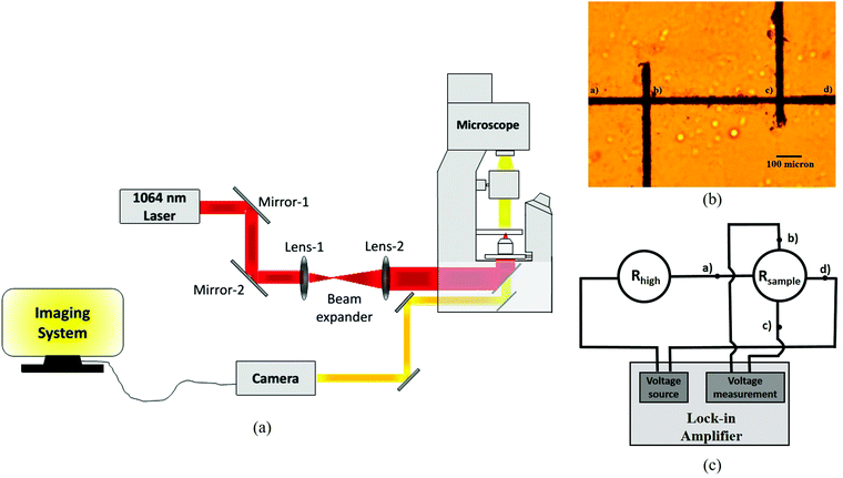 |
| | Fig. 1 (a) Schematic of our optical tweezers setup. (b) Typical Hall-bar structure made by patterning SOM + PPy/PAni. (c) Circuit diagram for measurement of conductivity. | |
Conductivity measurement technique
A standard 4-probe measurement technique was used to measure the resistance of the Hall-bar shaped patterns shown in Fig. 1(b). The dimensions of the patterns were found from images taken using a Scanning Electron Microscope (SEM) which we show in the subsequent figures. Very thin (0.1 mm) wire connections were made through Indium contacts at the positions a, b, c and d (Fig. 1(b)) of the Hall-bar. As shown in Fig. 1(c), a fixed current was passed through two opposite contacts (e.g., contact-a to contact-d) from a lock-in amplifier (SR830, Stanford Research Systems), by applying a suitable voltage difference at a low modulation frequency of around 20 Hz between the junctions, while a high resistance (controlled and tunable) was connected in series with the pattern. The voltage drop across the other two contacts (contact-b and contact-c in this case) was measured using the same lock-in amplifier at the reference frequency of 20 Hz. From this, we essentially measured the resistance between the positions b and c. Then, the current and voltage probes were interchanged and the measurements were repeated. For every sample, the whole process was performed for 3 sets of high resistances and 5 sets of currents for each resistance. This process is reliable and gives a precise measurement of the resistance, and we initially performed a benchmarking using standard resistances. To find the value of the measured resistance, we write the current through the circuit I as, I = Vin/(Rhigh + Rsample) ∼ Vin/Rhigh, since Rhigh ≫ Rsample. Thus, Rsample = Vsample/I. Vsample is directly measured by the lock-in amplifier, so that we finally have Rsample = (Vsample × Rhigh)/Vin. Note that to ensure that the approximation holds robustly, Rhigh should be at least 3 orders of magnitude greater than Rsample.
Results
A pictorial collage of the diverse patterns of SOMs + PPy/PANi that we have formed using our technique is demonstrated in Fig. 2. The bright field/SEM images demonstrate the range and versatility of our technique and the ability to control the shape and size of the patterns. The dimensions of the patterns are indicated in each picture. We are able to control the pattern width by varying the size of the bubble, which can be achieved by changing the laser power or the dwell-time of the laser at a particular spatial location.21 We show single linear patterns of different widths ranging from 45 μm (Fig. 2(a), which also has an inset showing two parallel linear patterns of only SOMs of width around 13 μm) to 6 μm (Fig. 2(b)) for SOMs + PPy, an annular disc pattern in SOMs + PPy with diameter ∼10 μm and thickness ∼4 μm (Fig. 2(c)), and the letter C written using SOMs + PAni of size ∼9 μm and thickness ∼3 μm (Fig. 2(d)). Note that discs are easily produced using our technique even without translation of the bubble since for a stationery bubble, the self assembly occurs around the bubble base in the shape of a disc21 – which is essentially the footprint of the bubble on the glass substrate where it is grown. The letter C is created during post-processing by carefully etching away a side of a disc by introducing very small quantities (few μl) of triethylamine – a weak base that dissolves the SOMs (which are acidic in nature) in the pattern – for a few seconds and drying under hot air immediately. Next, we show a double linear pattern of SOMs + PAni (Fig. 2(e)), with the thickness of individual patterns being about 4 μm, while the distance between each pattern is ∼1 μm. To demonstrate our control in the distances between the individual linear patterns, we inscribe a linear grid (Fig. 2(f)), where we vary the horizontal and vertical distances between 4–12 μm. The irregularities at the pattern edges are mostly due to the fact that the microscope stage is translated by a joystick manually, so that the inherent vibrations get coupled easily to compromise the quality of the pattern edges. This should be reduced considerably on automation of the microscope stage, which is, however, a technicality that we intend to address in future work. The thickness of the patterns can also be varied between 1–3.5 μm as we demonstrate in Fig. 2(g) and (h), where the thicknesses are 3.5 and 2 μm, respectively. The thickness depends on the laser dwell-time, which determines the extent of particle assembly around the bubble in all three dimensions. The minimum width of the pattern is limited presently by the laser wavelength, and it can certainly reach nanoscopic dimensions if conducting materials that have absorption at lower wavelengths can be used for patterning.21 We finally show an SEM image of the Hall-bar like structure of SOMS + PAni in Fig. 2(i) that we use to measure conductivity by the method described earlier.
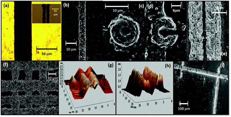 |
| | Fig. 2 (a) A single continuous linear pattern of SOMs + PPy. (Inset: Two parallel linear patterns of just SOMs) of width around 45 μm. (b) SEM image of a SOMs + PPy linear pattern of width around 6 μm. (c) SEM image of an annular disc pattern of SOMs + PPy of thickness around 4 μm. (d) The letter ‘C’ written using SOMs + PAni – the thickness is around 3 μm. (e) Two parallel linear patterns using SOMs + PPy – the gap between the patterns is around 1 μm, while the thickness of each pattern is about 4 μm. (f) A grid pattern of different spacings drawn out of SOMs + PAni. The vertical spacings vary from 11 μm (top row to middle row) to around 5 μm (middle row to bottom row), while the horizontal spacings are almost constant – around 10 μm. (g) AFM image of a double linear pattern of thickness 3.5 μm and width 20 μm. (h) AFM image of a double linear pattern of thickness 2 μm and width 20 μm. (i) SEM image of a pattern drawn in the form of a Hall bar structure of SOMs + PAni. The thicknesses of the patterns are around 80 μm. | |
The results of the conductivity measurements of the SOM + PPy (PAni) are shown in Fig. 3. The maximum conductivity of SOMs + PPy is ∼450 Siemens cm−1, while that of SOMs + PAni is ∼600 Siemens cm−1. Both values are significantly higher than that recorded in the literature, where the maximum reported values of conductivity for PPy and chemically doped PAni are within a range of 10–100 Siemens cm−1.13,14 In our experiments, we have varied the percentage concentration of SOMs in the initial dispersion with the monomers, and observed a certain value of SOM concentration where the conductivity is maximum. We attribute this to the fact that we synthesize various metal oxides (as described later) that act as dopants, which naturally implies that an optimum doping percentage would be required to obtain the highest conductivity. After the concentration of SOMs increases beyond a certain level, the metal oxides as well as PPy (PAni) are no longer formed so that the overall conductivity is dominated by that of the SOMs, which is obviously rather low. Note that the conductivity of patterns with only SOMs is around 50 Siemens cm−1, and we observe that we approach that value (as shown in Fig. 3(b)) when we keep on increasing the SOM percentage in the dispersion with the monomers. We now need to understand the reason behind the polymerization of the monomers in the presence of the SOMs, and the significantly higher values of conductivity we obtain than that reported earlier.
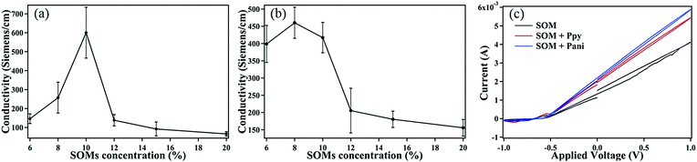 |
| | Fig. 3 (a) Measured conductivity of SOM + PPy patterns. (b) Measured conductivity of SOM + PAni patterns. (c) Cyclic voltammetry of SOM, SOM + Ppy & SOM + Pani patterns. | |
We also conducted cyclic voltammetry (CV) on the patterns (SOM, SOM + PPy, and SOM + PAni) to investigate their electrochemical properties. Each glass substrate with the respective pattern inscribed and contact wires connected is immersed in a KCl solution, and voltage is applied using a standard CV setup. The plots show a very small hysteresis loop as well as the absence of peaks which displays that the material is chemically inactive, which implies that their composition will not be modified on the application of voltage so that they can be used extensively in developing electronic circuits.
Discussion
In situ formation of polypyrrole, polyaniline, and metal oxides in the presence of SOMs in optical tweezers
We first demonstrated our technique of micro-bubble-induced patterning with SOMs.21 However, we also showed that other materials could be co-deposited with SOMs,21,27 which helped us in developing the catalytic chips discussed in ref. 27. We now use the same phenomenon in extending our technique towards patterning conducting materials. For initial proof-of-concept experiments, we chose polypyrrole (Ppy) and polyaniline (PAni), which are well-known conducting polymers. These polymers, especially PAni, have been used earlier to make solution printable electronics.20 The conductivity of the bare polymers is rather low, and is typically increased by chemical or metallic doping.15,16 However, there exists very few examples in the literature where synthesizing, doping, and patterning are carried out in a single step,36,37 starting from the parent monomers. Thus, we started our experiments by preparing a dispersion of SOMs with the individual monomer that we wanted to polymerize and co-deposit with the SOMs. We anticipated that we could observe direct polymerization due to the action of the trapping laser for the following reason – it is known that a SOM absorbs 1064 nm laser light and goes to the excited state (MoVI to MoVI*). This excited state species would oxidize pyrrole/aniline and itself get reduced to the MoV state, due to the high temperatures (around 350 °C, depending on the laser power38) prevalent near the base of the micro-bubble which is also the focal spot of the laser. MoV is further reduced to MoIV, which leads to the completion of the polymerization process. The oxidized pyrrole and aniline would then undergo polymerization following the general oxidative polymerization route as shown in Fig. 4(a). In other words, the initially oxidized monomer would be converted into a radical. This radical would now react with a monomer unit to form a dimer, which would further combine with another monomer unit to form a long chain polymer. At the end of the process, we have protonated polymers and metal oxide nano conjugates held together by mediation of the hydrogen bonds between metal oxide and the polymers, which, as we explain later, leads to the high conductance values we observe. This is exactly what we observe experimentally, which is first manifested in the color of the patterns after patterning. While SOM patterns are typically greyish in colour (as shown in the inset of Fig. 2(a)), the patterns of PPy and PAni with SOMs are black, as shown in Fig. 2(a). The definitive proofs of the formation of PPy or PAni are obtained after we characterize the linear patterns by HATR-IR spectroscopy. From the HATR-IR spectroscopy as shown in Fig. 4(b) and (c), we have obtained characterized peaks for PPy at 1460 cm−1 (C![[double bond, length as m-dash]](https://www.rsc.org/images/entities/char_e001.gif) C stretching of pyrrole ring), 1306 cm−1 (C–N stretching vibration in the ring), 1168 cm−1 (C–H in-plane deformation), 1012 cm−1 (N–H in-plane deformation), and 904 cm−1 (C–H out-of-plane deformation), respectively, which confirms the formation of polypyrrole in the pattern (Fig. 4(b),39,40). In the case of PAni (Fig. 4(c)), we have obtained peaks at 1559 cm−1 (PANI ring stretching), 1489 cm−1 (PANI benzenoid ring stretching), 1295 cm−1 (PANI C–N stretching C–H bending), and 1155 cm−1 (PANI C–N stretching C–C bending) which also confirms the formation of PAni from aniline.41,42 Thus, from the HATR spectra, it is clear that in the presence of the tweezers laser at 1064 nm, the SOMs catalyze the polymerization process of both pyrrole and aniline. We also confirm the generation of MoV in the reaction medium by performing UV-VIS spectroscopy of the catalyst solution after reaction. The UV-VIS spectrum, with a typical characteristic peak at close to 700 nm, reveals that a MoV type species is formed during the course of the reaction.43 The mechanism is further confirmed by adding catechol in the reaction medium. When catechol is added, the polymerization reaction is inhibited. This is due to the fact that catechol is more oxidizing than pyrrole and aniline, so that it gets oxidized by the SOMs more readily compared to the latter, thus preventing the polymerization from being initiated. It is thus confirmed that we have developed a novel mechanism for simultaneous polymerization and patterning, and we further probe the nature of the synthesized materials and attempt to explain their behaviour specifically regarding the very large conductivity observed, by a number of different spectroscopic and characterization processes as described below.
C stretching of pyrrole ring), 1306 cm−1 (C–N stretching vibration in the ring), 1168 cm−1 (C–H in-plane deformation), 1012 cm−1 (N–H in-plane deformation), and 904 cm−1 (C–H out-of-plane deformation), respectively, which confirms the formation of polypyrrole in the pattern (Fig. 4(b),39,40). In the case of PAni (Fig. 4(c)), we have obtained peaks at 1559 cm−1 (PANI ring stretching), 1489 cm−1 (PANI benzenoid ring stretching), 1295 cm−1 (PANI C–N stretching C–H bending), and 1155 cm−1 (PANI C–N stretching C–C bending) which also confirms the formation of PAni from aniline.41,42 Thus, from the HATR spectra, it is clear that in the presence of the tweezers laser at 1064 nm, the SOMs catalyze the polymerization process of both pyrrole and aniline. We also confirm the generation of MoV in the reaction medium by performing UV-VIS spectroscopy of the catalyst solution after reaction. The UV-VIS spectrum, with a typical characteristic peak at close to 700 nm, reveals that a MoV type species is formed during the course of the reaction.43 The mechanism is further confirmed by adding catechol in the reaction medium. When catechol is added, the polymerization reaction is inhibited. This is due to the fact that catechol is more oxidizing than pyrrole and aniline, so that it gets oxidized by the SOMs more readily compared to the latter, thus preventing the polymerization from being initiated. It is thus confirmed that we have developed a novel mechanism for simultaneous polymerization and patterning, and we further probe the nature of the synthesized materials and attempt to explain their behaviour specifically regarding the very large conductivity observed, by a number of different spectroscopic and characterization processes as described below.
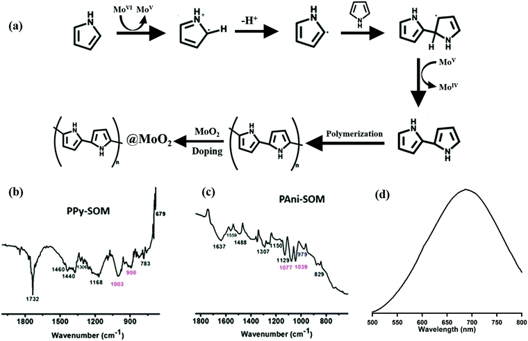 |
| | Fig. 4 (a) Possible reaction pathway of the polymerization process. (b) HATR-IR spectrum of the PPy + SOM pattern. (c) HATR-IR spectrum of the PAni + SOM pattern. (d) UV-VIS spectrum of the catalyst solution after reaction, i.e. after forming the patterns of SOM + PPy. The same is found in the case of SOM + PAni too. | |
Very high conductivity of PPy and PAni patterns
As we have shown earlier, the conductivity we measure of the patterned patterns is significantly higher than that reported in the literature. To understand this, we investigate the composition of the patterns more closely by performing further careful analysis of their IR spectra, XPS measurements of the patterns, EDX imaging of the patterns, and finally UV-VIS spectroscopy. We now describe these in detail:
Analysis of IR spectra.
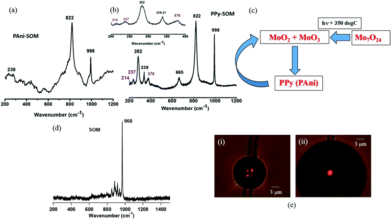
From the IR spectrum of the PPy-SOM patterns, we find that all the IR-active modes are shifted from the IR spectrum of pure PPy by a few cm−1. Among the peaks, those obtained due to C–N stretching and N–H in-plane deformation are shifted more in comparison with the other peaks. This is possibly due to the formation of hydrogen bonding between the N–H group of PPy and the oxygen of the molybdate. Besides this, the hydrogen bonding ionic interaction can also be present among these molecules, which causes the shift in the peaks of PPy. Similar peak shifts are observed in the case of the IR spectrum of the SOMs + PAni patterns compared to that of PAni alone. A greater shift in the C–N stretching modes is observed here as well, which is due to the presence of the ionic interaction between the molybdate and PAni. This clearly indicates that molybdate is doped in the polymer structures which results in their anomalously high conductivity. In fact, this also confirms our observation that an optimum amount of doping is necessary to obtain the highest conductivity as shown in Fig. 3. It is now worthwhile to understand the nature of the molybdate present in the pattern. This was accomplished with the help of the Raman spectra of the patterns of both PPy (Fig. 5(a)) and PAni (Fig. 5(b)). From the Raman spectra, we obtained three characteristic peaks at 998 cm−1, 822 cm−1 and 282 cm−1, which indicates the presence of MoO3 in the pattern. It is known from the literature that at elevated temperatures, heptamolybdate converts into MoO3.35,44–46 For our case, the temperature at the reaction point is estimated to be around 350 °C,38 which converts the heptamolybdate to MoO3, and thus explains the presence of MoO3, as we show in Fig. 5(c). But as MoO3 is a d0 system,47 the presence of the single free electron is unlikely to enhance the conductivity of the polymer material to the extent that we observe. Hence, it would be reasonable to assume that some other metal oxide species is present as a dopant within the pattern which contributes to enhancing the conductivity. Indeed, we obtained a small number of distinct peaks in the Raman spectrum at 376 cm−1, 237 cm−1 and 214 cm−1 which occur due to the presence of a further reduced molybdenum oxide, mainly MoO2, having the oxidation state MoIV, as is shown in Fig. 5(a) and (b). The formation of MoO2 is also confirmed from the reaction mechanism of oxidative polymerization of pyrrole and aniline. Indeed, to complete the polymerization process, a two-step reduction needs to occur for the catalyst: in the first step MoVI is reduced to MoV which is further reduced to MoIV. The formation of the reduced molybdenum species is also confirmed from a UV-VIS spectrum (Fig. 5(d)), where the peak at around 700 nm indicates the formation of a molybdenum blue type species during the formation of the pattern. Thus, both MoIV and MoV oxides are doped within the polymer material. The doping of MoIV and MoV oxides on the polymer material enhances their conductivity as the former contains two and the latter one free electron(s), respectively. The presence of these free electrons reduces the band-gap energy of the species, which becomes much lower than that of the conductive polymers alone. Therefore, these polymer materials possess a significantly higher conductivity compared to pure PPy and PAni, or even that achieved by doping these species chemically,15 or with carbon nanotubes.16
 |
| | Fig. 5 Raman spectra of (a) PAni and (b) PPy, indicating the presence of MoO3 and other reduced molybdates in the pattern. (c) Possible mechanism of conversion of heptamolybdate to reduced molybdenum species. (d) Raman spectrum of only SOM patterns. (e) (i) A bubble grown in an SOM dispersion from a pre-existing SOM pattern at an input laser power of 50 mW. The image is taken 1 second after the bubble is formed. (ii) A bubble grown in an SOM + PPy dispersion – all other conditions remain the same as in (i). | |
XPS data.
We confirmed our hypothesis regarding the material composition of our patterns by performing XPS spectroscopy of the patterns of SOM, SOM + PAni and SOM + PPy using a synchroton source in conjunction with an AIPES (Angle Integrated Photo-Electron Spectroscopy) system. The electron beam was made incident on the patterns and the spectra were recorded. The XPS spectra of the corresponding elements in different cores were fitted where the contributions from different species including adventitious effects were taken into account. These include stray contributions due to Si48 (Si 2s & Si 2p) and Ag49,50 (Ag 3d) where the former appeared due to the glass cover-slip background on which patterns were made and the latter was due to silver paste which was used to attach the samples with the mount to perform XPS. Similarly, stray C was observed in the spectra for SOMs – a part of which we attribute to contamination of the patterns with CH3OH, which we use for cleaning up the samples, while a part was due to the presence of stray C in the set-up itself which also appeared in a spectrum we recorded (not shown here) to probe the background effects.
The spectra with the associated fits to extract the peak binding energy values of each elemental species are provided in Fig. 6. We provide both the survey scans of each pattern (Fig. 6a(i), b(i) and c(i) for SOM, SOM + PAni, and SOM + PPy, respectively), as well as the zoomed-in spectra of different cores of elements, C, Mo, O, and N (Fig. 6a(ii)–(iv), b(ii)–(v) and c(ii)–(v), present in the three different patterns). The area under the curve for different contributory species was determined. From the relative ratios of area under the curves of the contributory species, we determine the relative percentage of different elements present in the corresponding core, where the multiplicity factor (2 O in MoO2, 3 O in MoO3) was taken into account. It is interesting to note that N was not obtained in the SOM spectra at all, as is apparent in Fig. 6(a)(i). This can be attributed to the fact that N is added to the patterns only due to the formation of PPy and PAni. In the C spectra (Fig. 6a(ii), b(ii) and c(ii)), we had contributions from CH3OH and adventitious carbon. However, the peak heights were considerably higher in the patterns with PPy and PAni than that for SOMs alone, which is due to the presence of the C-ring (C 1s) in PAni (Fig. 6b(ii)51) and PPy (Fig. 6c(ii)52)
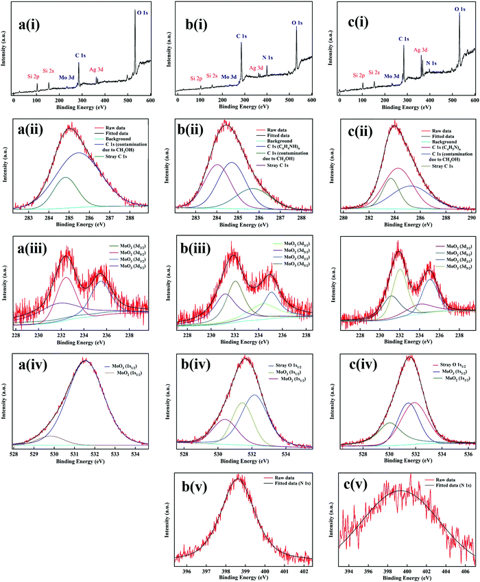 |
| | Fig. 6 (a) XPS spectra of an SOM pattern, a(i) survey scan, a(ii) C spectra, a(iii) Mo spectra, a(iv) O spectra. (b) XPS spectra of an SOM + PAni pattern, b(i) survey scan, b(ii) C spectra, b(iii) Mo spectra, b(iv) O spectra, b(v) N spectra. (c) XPS spectra of an SOM + Ppy pattern, c(i) survey scan, c(ii) C spectra, c(iii) Mo spectra, c(iv) O spectra, c(v) N spectra. The red curves are the fit to the observed peaks performed in the software XPSPEAK41. | |
We now analyze in detail the Mo spectra shown in Fig. 6a(iii), b(iii) and c(iii). Note that we excluded the stray contributions due to adventitious effects while comparing conversion rates of MoO2 and MoO3 from the initial state (MoO7). In the Mo spectra (Fig. 6a(iii), b(iii) and c(iii)) we have contributions from MoO353 and MoO2.54 For both species, two doublets (3d3/2 and 3d5/2) are present due to spin–orbit coupling, with the ratio of the areas of the individual peaks in the doublets fixed at a ratio of 2:3 in accordance with the selection rules. Note that in MoO3 the oxidation state of Mo is +6 (Mo+6), whereas in the case of MoO2 the oxidation state of Mo is +5 (Mo+5). Thus, MoO3 gets reduced into MoO2 as PPy and PAni are formed and resultantly, the conductivity increases with increase in MoO2 in the pattern. For the fitting, we used the XPSPEAK41 software, where we kept the binding energy values (peak centers) of each peak of MoO2 and MoO3 and the ratio of the peak areas fixed, and fit 2 Gaussian peaks and determined the relative percentages of the oxide species from the fitted peak areas. The relative percentages for patterns with SOMs, SOM + PAni, and SOM + PPy are presented in Table 1. For a consistency check, we determined the relative percentage of the oxides from the spectra obtained from both Mo and O cores,55,56 and while these matched very well for SOM and PAni, the values were slightly different for PPy, which may be due to stray O which may have appeared in the O-core measurements for the latter. It is clear that the ratio of MoO2:MoO3 is 10–12 times higher in the PPy and PAni patterns compared to that in the SOM, which explains the high conductivity in the latter, since it is indeed the presence of MoO2 which is responsible for high conductivity. Interestingly, the ratio of MoO2:MoO3 between PAni and PPy is 1.38:1, which is very close to the difference in conductivity we observe in them (around 1.33:1 as mentioned in the Results section). This gives credence to our understanding of the chemistry of the phenomenon we report here (Fig. 6).
Table 1 Percentage of MoO2 and MoO3 in SOM, SOM + PPy, and SOM + PPy. Percentage values from both O-core and Mo-core XPS spectra are shown
| Species |
MoO2 (%) |
MoO3 (%) |
| SOM (Mo-core) |
8.0 |
91.98 |
| SOM (O-core) |
6.93 |
93.07 |
| SOM + PAni (Mo-core) |
50.61 |
49.39 |
| SOM + PAni (O-core) |
51.86 |
48.14 |
| SOM + Ppy (Mo-core) |
39.2 |
60.8 |
| SOM + Ppy (O-core) |
47.12 |
52.88 |
Low conductivity of SOM patterns.
A question naturally arises as to why we do not observe the formation of MoO2 and MoO3 in the case of patterns of pure SOMs. The reason actually underlines the synergistic nature of the phenomenon we observe in the presence of pyrrole (aniline) in our sample dispersion. As mentioned earlier, and shown in Fig. 5(c), the formation of the metal oxides occurs only at temperatures of around 350 °C. Such a temperature is indeed reached at the laser focal point where the bubble originates, both in the case of pure SOMs and that of SOMs + pyrrole (aniline) at laser powers (measured before the microscope objective) of about 90 and 30 mW for the former and the latter, respectively. While we do not measure the temperature at the laser focal spot directly, we use the fact that water cannot exist as a fluid at temperatures higher than 647 K (374 °C).38 We then carry out a numerical simulation where we solve the heat equation to predict the size of the bubble at a certain temperature of the hot spot, which we then match with experiments where we measure the size of the bubble at different laser powers.38 Thus, we are able to obtain a conversion between laser power and temperature of the hot spot, and can set the laser power to a certain optimum value to attain a particular bubble size for a preferred pattern dimension. Now, the high temperature of the hot spot leads to the conversion of heptamolybdate to the metal oxides in the bubble vicinity. However, in the case of the heterogeneous dispersion, the formation of the metal oxides also initiates the redox reaction that causes the formation of PPy (PAni). Note that the thermal conductivity of PPy/PAni is substantially higher than that of pure SOMs. As a result, the temperature at the focal point dissipates at a much faster rate in this case than that of SOMs alone, so that the entire region near the vicinity of the bubble reaches a temperature close to that at the focal point. This is elucidated by the significantly faster growth of the bubble in a SOM/PPy (PAni) dispersion compared to a SOM dispersion (with the initial conditions and laser power used being the same in both cases) as we show in Fig. 5(d) and Videos 1 and 2 (ESI†). This leads to further conversion of heptamolybdate to MoO2 and MoO3 near the bubble in the former which, however, does not occur in the latter due to lower thermal conductivity of the SOMs. The formation of the metal oxides in turn causes further conversion of PPy (PAni), and the cycle continues in synergy. Thus, the patterns in SOMs + pyrrole (aniline) are doped to a much larger extent by the metal oxides (along with the presence of the conductive polymers) than that for SOMs alone, which naturally leads to the significantly higher conductivity. This is borne out by the fact that the Raman spectra of the SOMs alone have no traces of either MoO2 or MoO3, as we show in Fig. 5(e). In short, we have a completely synergistic synthesis with the light-induced initial high temperature creating the materials, and the materials in turn facilitating the high temperature that continues to drive the process.
SEM + EDX imaging of the patterns.
In order to determine the heterogeneity of our photopolymerization process, as well as to visualize the dispersability of the SOM within the conducting polymer matrix, we resorted to SEM + EDX imaging of the patterns. A representative image for the results is shown in Fig. 7. We display the EDX mapping of the elements Mo, O, C, and N for patterns of SOM, SOM + PPy, and SOM + PAni in the regions within the boundary boxes in purple shown on the individual SEM images of the patterns. It is clear from the mapping images that all elements are very well dispersed in the patterns. However, we observe that the concentrations of C and N are extremely small in the SOM patterns, so that we chose not to display their EDX mappings in the figure. Thus, we can conclude that photopolymerization leads to a heterogeneous material where the SOMs are evenly dispersed within the polymer matrices.
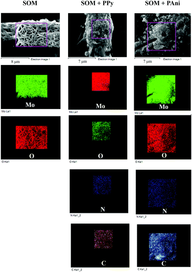 |
| | Fig. 7 EDX of SOM (first column), SOM + PPy (second column), and SOM + PAni (third column). The elemental distribution of different species in a selected area of the EDX image (demarcated as a purple rectangle) for each pattern is shown below. | |
Conversion efficiency of PPy and PAni.
An important issue for us was to attempt to quantify the amount of pyrrole/aniline converted to their polymeric forms. This was non-trivial since we deal with microscopic amounts here, and also since we do not use up the entire dispersion to construct a single pattern. In fact, the amount of conversion would be directly dependent on the size of the pattern – basically, its dimensions in all three directions. However, for a ballpark estimate, we used a typical pattern of width 30 μm, depth 1.5 μm, and length 2 mm. We noted the input volumes of pyrrole and aniline added to the dispersion, and after the pattern was completed, we carefully pipetted off the dispersion remaining in the sample chamber. Thus, we noted that we could recover around 50% of the input volume for both pyrrole and aniline in their liquid dispersion form. However, a little bit was also adsorbed on the inside surface of the chamber. Now, from the XPS data, we notice that the peak for N57,58 (which arises solely due to the presence of PPy/PAni in the patterns) is considerably stronger for PAni (Fig. 6b(v)) compared to PPy (Fig. 6c(v)), with the area of the former being 2334 AU (arbitrary units), and that of the latter being 1061 AU. This implies that the conversion efficiency for PAni is about 45% more than that for PPy. We can indeed attribute the higher conversion efficiency for PAni to the fact that aniline has a higher boiling point (184.1 °C) which is around 42.5% higher than that of pyrrole (129 °C). Thus, more pyrrole is evaporated when it comes in close proximity to the hot spot thus preventing conversion to PPy. This also explains the larger amount of MoO2 formed in PAni compared to PPy (the measured number from the Mo-core XPS data as noted in Table 1 is 30.5% higher in PAni) – which is due to the fact that the larger amount of PAni present increases the thermal conductivity in the vicinity of the hot spot that leads to more efficient conversion of heptamolybdate to the corresponding metal oxides. This is also responsible for the higher conductivity of the PAni patterns compared to those of PPy. Thus, we could finally conclude that around 20–40% of pyrrole/aniline was converted to their respective polymeric forms in a linear pattern of dimensions 30 μm × 2 μm × 2 mm, with the yield of PAni being around 45% higher than that of PPy. Finally, it is clear that we lose a certain amount of the initial mass of the input monomers, as well as that of the conducting polymers – which according to a recent estimate is around 32% between temperatures of 200–700 °C.59 However, the maximum temperatures we reach being only 350 °C, it is likely that the mass loss in our case is lower.
Conclusions
In conclusion, we demonstrate for the first time simultaneous synthesis, doping, and patterning of conducting materials in an optical tweezers configuration employing directed self-assembly mediated by a thermo-optic tweezers-induced micro-bubble. Our approach essentially employs green chemistry techniques, where we start off with simple aqueous dispersions of monomers that are subsequently photopolymerized in the presence of SOMs, which also leads to the additional synthesis of metal oxides. We demonstrate this technique separately on pyrrole and aniline. Starting from an aqueous dispersion of the monomer(s) with the SOMs which is irradiated in an optical tweezers configuration by a laser of wavelength 1064 nm, we excite the SOMs from (MoVI to the excited state MoVI*), so that with the occurrence of simultaneous and synergistic redox processes, we are able to synthesize the conductive polymers and PPy and PAni, as well as metal oxides (MoO3 and MoO2). We then draw diversely shaped patterns of the same by translating the bubble using the translation stage of the tweezers microscope. We can control the pattern dimensions to a precision of around 1 μm presently (limited by diffraction of the focused laser), and have achieved a minimum pattern width of 3 μm which can be extended to several tens of microns quite controllably. We measure the conductivity of the synthesized materials to be around 450 Siemens cm−1 for PPy and 600 Siemens cm−1 for PAni, both values being more than an order of magnitude higher than that obtained for the respective polymers in earlier work. We attribute this to the doping of the conductive polymers by the metal oxides, and verify the presence of all the species by XPS, EDX, Raman, HATR-IR, and UV-VIS spectroscopy. This method can thus be used to pattern complex electronic circuits using solution processing, and can in general be extended to the fabrication of electronic devices, micro-capacitors, etc. We have indeed commenced work in developing micro-capacitors, and have measured the basic capacitance of SOM patterns to be ∼ a few picofarads. Thus, we assume that with the help of suitable dielectrics sandwiched between parallel linear patterns of suitable polyoxometalates, we should be able to develop micro-capacitors based on our technique. Finally, the ease and simplicity of the technique, coupled with the perfectly synergistic mechanism to achieve complex, high-conductivity material synthesis are additional advantages, which thus makes it a good candidate to qualify as a new micro-lithographic tool for fabricating solution processed electronic circuits and devices.
Author contributions statement
SG and SD carried out the experiments and synthesis of materials. The idea was envisaged by SR and AyB, who also wrote the paper. SP, PT, and BR helped in initial experiments. PM helped in the electronic conductivity measurements.
Acknowledgements
The authors would like to acknowledge IISER, Kolkata for providing funding and laboratory facilities, CSR Indore for providing us access to the Indus-1 beamline which facilitated the XPS measurements, Dr R. J. Choudhary and Mr A. Wadikar of CSR Indore, and Dr S. Majumdar and Dr T. Ganguli of RRCAT, Indore, for helping us with the XPS experiments. SR acknowledges DST Fast Track and BRNS, DAE, India for financial assistance. SG acknowledges DST INSPIRE for a fellowship.
References
- M. Grzelczak, J. Vermant, E. M. Furst and L. M. Liz-Marzan, ACS Nano, 2010, 4, 3591–3605 CrossRef CAS PubMed.
- Y. Lin, A. Boker, J. He, K. Sill, H. Xiang, C. Abetz, X. Li, J. Wang, T. Emrick, S. Long, Q. Wang, A. Balazs and T. P. Russell, Nature, 2005, 434, 55–59 CrossRef CAS PubMed.
- S. J. Zhen, Z. Y. Zhang, N. Li, Z. D. Zhang, J. Wang, C. M. Li, L. Zhan, H. L. Zhuang and C. Z. Huang, Nanotechnology, 2013, 24, 055601 CrossRef PubMed.
- H. Duan, D. Wang, D. G. Kurth and H. Möhwald, Angew. Chem., Int. Ed., 2004, 43, 5639–5642 CrossRef CAS PubMed.
- S. Fujii, K. Kanaizuka, S. Toyabe, K. Kobayashi, E. Muneyuki and M. aki Haga, Langmuir, 2011, 27, 8605–8610 CrossRef CAS PubMed.
- S. N. Varanakkottu, M. Anyfantakis, M. Morel, S. Rudiuk and D. Baigl, Nano Lett., 2016, 16, 644–650 CrossRef CAS PubMed.
- S. Mann, Nat. Mater., 2009, 8, 781–792 CrossRef CAS PubMed.
- H. Fan, K. Yang, D. M. Boye, T. Sigmon, K. J. Malloy, H. Xu, G. P. López and C. J. Brinker, Science, 2004, 304, 567–571 CrossRef CAS PubMed.
- T. A. Gschneidtner, Y. A. Diaz Fernandez and K. Moth-Poulsen, J. Mater. Chem. C, 2013, 1, 7127–7133 RSC.
- S. G. Rao, L. Huang, W. Setyawan and S. Hong, Nature, 2003, 425, 36–37 CrossRef CAS PubMed.
- C. Joachim, J. K. Gimzewski and A. Aviram, Nature, 2000, 408, 541–548 CrossRef CAS PubMed.
- Y.-Y. Noh, N. Zhao, M. Caironi and H. Sirringhaus, Nat. Nano, 2007, 2, 784–789 CrossRef CAS PubMed.
- N. V. Blinova, J. Stejskal, M. Trchová, J. Prokes and M. Omastová, Eur. Polym. J., 2007, 43, 2331–2341 CrossRef CAS.
- H. Kang and K. Geckeler, Polymer, 2000, 41, 6931–6934 CrossRef CAS.
- C. K. Chiang, C. R. Fincher Jr, Y. W. Park, A. J. Heeger, H. Shirakawa, E. J. Louis, S. C. Gau and A. G. MacDiarmid, Phys. Rev. Lett., 1977, 39, 1098–1101 CrossRef CAS.
- A. L. Cabezasa, Y. Fenga, L.-R. Zhenga and Z.-B. Zhang, Carbon, 2013, 59, 270–277 CrossRef.
- M. Reyes-Reyes, I. Cruz-Cruz and R. López-Sandoval, J. Phys. Chem. C, 2010, 114, 20220–20224 CAS.
- J. J.-S. Rickard, I. Farrer and P. G. Oppenheimer, ACS Nano, 1986, 10, 3865–3870 CrossRef PubMed.
- N. Aydemir, J. Parcell, C. Laslau, M. Nieuwoudt, D. E. Williams and J. Travas-Sejdic, Macromol. Rapid Commun., 2013, 34, 1296–1300 CrossRef CAS PubMed.
- A. C. Arias,
et al.
, Chem. Rev., 2010, 110, 3 CrossRef CAS PubMed.
- B. Roy, M. Arya, P. Thomas, J. K. Jürgschat, K. V. Rao, A. Banerjee, C. M. Reddy and S. Roy, Langmuir, 2013, 29, 14733–14742 CrossRef CAS PubMed.
- S. Roy, L. C. Bossers, H. J. Meeldijk, B. W. Kuipers and W. K. Kegel, Langmuir, 2008, 24, 666–669 CrossRef CAS PubMed.
- S. Roy, Comments Inorg. Chem., 2011, 32, 113–126 CrossRef CAS.
- S. Das, S. Biswas, T. Balaraju, S. Barman, R. Pochamoni and S. Roy, J. Mater. Chem. A, 2016, 4, 8875–8887 CAS.
- S. Das and S. Roy, RSC Adv., 2016, 6, 37583–37590 RSC.
- S. Roy, CrystEngComm, 2014, 16, 4667–4676 RSC.
- P. Thomas, C. Pei, B. Roy, S. Ghosh, S. Das, A. Banerjee, T. Ben, S. Qiu and S. Roy, J. Mater. Chem. A, 2015, 3, 1431–1441 CAS.
- S. Herrmann, C. Ritchie and C. Streb, Dalton Trans., 2015, 44, 7092–7104 RSC.
- M. Genovese and K. Lian, Curr. Opin. Solid State Mater. Sci., 2015, 19, 126–137 CrossRef CAS.
- X. Zou, Y. Shen, Z. Peng, L. Zhang, L. Bi, Y. Wang and S. Dong, J. Electroanal. Chem., 2004, 566, 63–71 CrossRef CAS.
- P. Anastas and N. Eghbali, Chem. Soc. Rev., 2010, 39, 301–312 RSC.
- G. Ćirić-Marjanović, Synth. Met., 2013, 177, 1–47 CrossRef.
- M. Can, H. Özaslan, N. Ö. Pekmez and A. Yldz, Polymer, 2004, 45, 7011–7016 CrossRef CAS.
- D. V. Brezoi, Am. J. Sci. Arts, 2010, 1, 53–58 Search PubMed.
- M. Dieterle, G. Weinberg and G. Mestl, Phys. Chem. Chem. Phys., 2002, 4, 812–821 RSC.
- A. D. Carswell, E. A. O'Rea and B. P. Grady, J. Am. Chem. Soc., 2003, 125, 14793–14800 CrossRef CAS PubMed.
- Y. Sun, B. T. Mayers and Y. Xia, Nano Lett., 2002, 2, 481–485 CrossRef CAS.
- B. Roy, M. Panja, S. Ghosh, S. Sengupta, D. Nandy and A. Banerjee, New J. Chem., 2016, 40, 1048–1056 RSC.
- M. A. Chougule, S. G. Pawar, P. R. Godse, R. N. Mulik, S. Sen and V. B. Pati, Soft Nanosci. Lett., 2011, 1, 6 CrossRef CAS.
- M. Nicho and H. Hu, Sol. Energy Mater. Sol. Cells, 2000, 63, 423–435 CrossRef CAS.
- J. Tang, X. Jing, B. Wang and F. Wang, Synth. Met., 1988, 24, 231–238 CrossRef CAS.
- M. Ohira, T. Sakai, M. Takeuchi, Y. Kobayashi and M. Tsuji, Synth. Met., 1987, 18, 347–352 CrossRef CAS.
- S. Das, P. Thomas and S. Roy, Eur. J. Inorg. Chem., 2014, 4551–4557 CrossRef CAS.
- A. Chithambararaj, D. B. Mathi, N. R. Yogamalar and A. C. Bose, Mater. Res. Express, 2015, 2, 055004 CrossRef.
- O. Lupan, V. Trofim, V. Cretu, I. Stamov, N. N. Syrbu, I. Tiginyanu, Y. K. Mishra and R. Adelung, J. Phys. D: Appl. Phys., 2014, 47, 085302 CrossRef.
- G. Solferino and A. J. Anderson, Chem. Geol., 2012, 322–323, 215–222 CrossRef CAS.
- D. O. Scanlon, G. W. Watson, D. Payne, G. Atkinson, R. Egdell and D. Law, J. Phys. Chem. C, 2010, 114, 4636–4645 CAS.
- M. Anwar, C. Hogarth and R. Bulpett, J. Mater. Sci., 1990, 25, 1784–1788 CrossRef CAS.
- G. B. Hoflund, J. F. Weaver and W. S. Epling, Surf. Sci. Spectra, 1994, 3, 151–156 CrossRef CAS.
-
C. D. Wagner and G. Muilenberg, Handbook of X-ray photoelectron spectroscopy, Perkin-Elmer, 1979 Search PubMed.
- S. Golczak, A. Kanciurzewska, M. Fahlman, K. Langer and J. J. Langer, Solid State Ionics, 2008, 179, 2234–2239 CrossRef CAS.
- J. Tabačiarová, M. Mičušk, P. Fedorko and M. Omastová, Polym. Degrad. Stab., 2015, 120, 392–401 CrossRef.
- J. Swiatowska-Mrowiecka, S. de Diesbach, V. Maurice, S. Zanna, L. Klein, E. Briand, I. Vickridge and P. Marcus, J. Phys. Chem. C, 2008, 112, 11050–11058 CAS.
- B. Wang, Y. Sasaki, S. Ikari, K. Kimura and T. Ito, Chem. Lett., 1987, 1955–1958 CrossRef CAS.
- F. Jahan and B. Smith, J. Mater. Sci., 1992, 27, 625–636 CrossRef CAS.
- T. A. Patterson, J. C. Carver, D. E. Leyden and D. M. Hercules, J. Phys. Chem., 1976, 80, 1700–1708 CrossRef CAS.
- E. Kang, K. Neoh, X. Zhang, K. Tan and D. Liaw, Surf. Interface Anal., 1996, 24, 51–58 CrossRef CAS.
- K. Neoh, E. Kang and K. Tan, Thermochim. Acta, 1990, 171, 279–291 CrossRef CAS.
- N. Su, Nanoscale Res. Lett., 2015, 10, 301 CrossRef PubMed.
Footnote |
| † Electronic supplementary information (ESI) available: Video1.avi, Video2.avi, Video titles.doc. See DOI: 10.1039/c7tc01941f |
|
| This journal is © The Royal Society of Chemistry 2017 |

 Open Access Article
 This Open Access Article is licensed under a
  a,
Preethi
Thomas
b,
Basudev
Roy
a,
Partha
Mitra
a,
Soumyajit
Roy
a,
Preethi
Thomas
b,
Basudev
Roy
a,
Partha
Mitra
a,
Soumyajit
Roy


