
 Open Access Article
 This Open Access Article is licensed under a
 Creative Commons Attribution 3.0 Unported Licence
Insights into chemical doping to engineer the carbon nanotube/silicon photovoltaic heterojunction interface†
L.
Yu
 ,
T.
Grace
,
M.
Batmunkh
,
M.
Dadkhah
,
C.
Shearer
and
J.
Shapter
*
,
T.
Grace
,
M.
Batmunkh
,
M.
Dadkhah
,
C.
Shearer
and
J.
Shapter
*
Centre for Nanoscale Science and Technology, School of Chemical and Physical Sciences, Flinders University, Bedford Park, South Australia 5042, Australia. E-mail: joe.shapter@flinders.edu.au
First published on 25th October 2017
Abstract
Graphene oxide/single-wall carbon nanotube (GOCNT) hybrid films have been used to fabricate heterojunction solar cells with silicon (Si) due to their compatibility with both aqueous and organic processing. In these cells GOCNT films are required to be both highly transparent and conducting. Different approaches are used to improve these optoelectronic properties of the GOCNT films, including hybridization with silver nanowires (AgNWs) and p-type doping with CuCl2, AuCl3, SOCl2, HCl, H2SO4, HNO3 and HClO4. UV-vis-NIR absorbance, Raman spectroscopy, and the sheet resistance of the films were used to evaluate the properties of the treated films and quantify doping. The most effective way to improve the optoelectronic properties of the GOCNT films was the incorporation of AgNWs which improved the figure of merit (FOM, the ratio of transparency and conductivity) by over 600%. However, GOCNT/Si heterojunction photovoltaic devices with HNO3 doped GOCNT films showed the highest solar photocurrent conversion efficiency (11.38 ± 0.26%). In terms of stability, CuCl2 and HCl doped films have the best electrode FOM stability, and devices made with such films have the most stable efficiency as well. This report suggests that the electronegativity of the active elements in the dopants has a strong influence on the optoelectronic properties of the films as well as the solar cell performance.
1. Introduction
Carbon nanomaterial based transparent conducting films are a potential alternative to replace the currently used transparent conductive oxides (such as indium doped tin oxide, ITO) which present several drawbacks1 including scarcity of indium,2 their brittle structure,3 instability in acid environments and high production costs.4 Carbon nanotubes (CNTs) are one example of a carbon nanomaterial famous for their unique optical and excellent electrical properties which enable the CNT-based thin films to be transparent and conductive at the same time.5–11 However, the hydrophobicity and the strong van der Waals interaction between individual nanotubes limit their compatibility with aqueous processing.12–15 Different dispersing agents which have both hydrophobic and hydrophilic moieties, such as polymers,16 porphyrins,17 cellulose derivatives,18 surfactants19 and single stranded DNA sequences,20 are commonly used to address this issue, but the liquid processing of the CNT films prepared from these aqueous dispersions often does not yield films with a high figure of merit (FOM).21Recently, graphene oxide (GO) has been shown to be able to both help to disperse CNTs in water and enhance the aqueous compatibility of the as-prepared film due to its amphiphilic nature.22–25 Such hybrid films made with GO and CNTs (GOCNTs) have been used as transparent window electrodes and applied on silicon to fabricate graphene oxide carbon nanotube/silicon heterojunction solar cells (GOCNT/Si).26 Briefly, in a typical device formed with p-type GOCNT films as the window electrode and an n-type silicon base, the silicon is the light absorbing layer which produces excitons. The resulting excitons are then separated into charge carriers under the influence of the built-in potential at the interface of the heterojunction, as shown in Fig. 1(a).27–31 Holes are transported through the GOCNT network acting as a window electrode and collected by the front metal electrode while electrons are collected at the back metal contact via the silicon layer.21 The exact nature of the heterojunction is still not clear although it has been discussed thoroughly in the recent literature.32–37 It can be regarded as a Schottky barrier, a metal–insulator–semiconductor or a p–n junction. In some cases, the thin silicon oxide layer between Si and GOCNTs improves the device performance via a reduction in the reverse saturation current.38
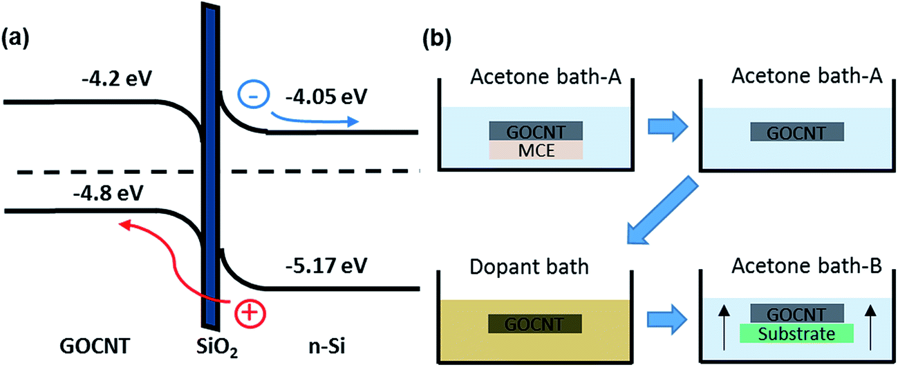 | ||
| Fig. 1 (a) Schematic energy diagram of GOCNT/Si heterojunction solar cells; (b) schematic of the bath doping process. MCE is the mixed cellulose ester filter and the substrate can be a glass slide or Si substrate coated with metal electrode. The filter paper dissolves in acetone and the GOCNT electrodes are then transferred to a dopant bath to conduct chemical doping. The GOCNT film is picked up with the substrate after being transferred to the next acetone bath. The band gap of GOCNT is estimated from the S11 peak position of the UV-vis-NIR spectra of the GOCNT films.32 | ||
In these solar cells, devices made with the as-deposited CNT films typically show mediocre performance due to high sheet resistance and low native p-doping. Chemical doping of the CNT film is normally performed to satisfy the practical requirements of the optoelectronic properties of CNT based window electrodes.39 The general p-type dopants include HCl,40 HNO3,41 H2SO4,42 SOCl2,43 AuCl3,44 and CuCl2.37 The sheet resistance (Rsheet) of CNT based networks is dependent on the conductivity of individual CNTs as well as the contact resistance between CNTs.1 Chemical doping results in the shifts of the Fermi level, which can increase the density of charge carriers and reduce the Schottky barrier height, ϕB, between metallic and semiconducting species, and as a result, the optical absorption peak caused by the first and second interband transitions in SWCNTs is suppressed or completely bleached (as shown in Fig. S1†).45 Recently, a bilayer structure of AgNWs/SWCNTs has been used to improve the efficiency of SWCNT/Si devices by nearly two-fold (from 4.31 to 7.89%) and the main improvement was attributed to the dramatic improvement of the optoelectronic properties with the addition of the AgNW top layer which provides highly conducting paths between CNTs.33,46
In this report, different p-type dopants as well as AgNWs are used to improve the optoelectronic properties of the CNT-based (GOCNT) transparent conducting films. Bath doping, as shown in Fig. 1(b), was used due to the benefit of the previously developed organic–aqueous transfer process making the films available for bath processing.21 This approach increases the doping period compared to simply dropping the chemicals on the films and eliminates the effect of the chemicals on the metal coated Si substrates (for example, the acid might dissolve the Cr layer) at the same time. AgNWs, due to their limited dispersity in water, could not be processed this way and they were filtered with GOCNTs on filter papers. The treated transparent films were then deposited on n-type Si to create GOCNT/Si heterojunction solar cells. Both the efficiency and the stability of the devices were studied and compared.
2. Experimental details
2.1 Preparation of stock solutions
GO was prepared following the improved synthesis based on Hummers' method reported by Marcano et al. with minor modifications as shown in the ESI.†47 The final concentration of the GO aqueous dispersion was kept at 1 mg mL−1. The GOCNT suspension was fabricated by following our previous report with the ideal mass ratio of GO![[thin space (1/6-em)]](https://www.rsc.org/images/entities/char_2009.gif) :CNT to be 1:2.25 (this ratio produces films that have excellent optoelectronic properties which can be used as transparent conducting electrodes)26 and the details are shown in the ESI.†
:CNT to be 1:2.25 (this ratio produces films that have excellent optoelectronic properties which can be used as transparent conducting electrodes)26 and the details are shown in the ESI.†
AgNWs were synthesized by following a typical polyol approach with slight modifications with the UV-vis spectrum and SEM images shown in Fig. S2.†48 The final concentration of AgNWs in water is 0.2 mg mL−1.
The redox colloidal solution (CuCl2 (99.0%, Sigma-Aldrich)/Cu(OH)2), (denoted as CuCl2 in the following section since Cu2+ in CuCl2 has been reported to be the active part for rapid p-type doping of SWCNTs by extracting electrons and being reduced to Cu1+ while Cu2+ hydroxide provides long-term doping stability)37 was prepared by adding a 1 M NaOH (98.0%, Chem-Supply) aqueous solution into a 0.1 M CuCl2 ethanol solution gradually. The volume ratio of these two solutions was kept at 1:2000.
118 mg of HAuCl4·3H2O (99.0%, Sigma-Aldrich) was dissolved in 30 mL of acetone at room temperature with gentle vortex mixing to prepare 10 mM AuCl3 solution. 10% v/v SOCl2 (99.0%, Sigma-Aldrich) was prepared by the dilution of pure SOCl2 with benzene. 10 wt% HCl (32.0%, RCI Labscan), 10 wt% HNO3 (70.0%, RCI Labscan), 10 wt% H2SO4 (98.0%, RCI Labscan) and 10 wt% HClO4 (70.0%, Merck) were prepared by dilution with deionized water.
2.2 Fabrication and treatment of transparent conducting hybrid films
The preparation of GOCNT hybrid films follows the procedure previously reported with slight modifications.21 In detail, 200 μL of the GOCNT initial suspension was diluted to 100 mL with deionized water for vacuum filtration. A 45 mm diameter mixed cellulose ester filter membrane (MCE, 0.45 μm, HAWP, Millipore, Australia) was used to collect GO and CNTs, and beneath the MCE membrane was a nitrocellulose membrane (25 nm, VSWP, Millipore, Australia) with four circular holes (0.49 cm2 each) so that a faster flow rate in the areas of four holes resulting from the different pore sizes in these two membranes produced four identical GOCNT hybrid films on the MCE during one filtration. After being dried under ambient conditions, each individual GOCNT hybrid film on the filter membranes was cut with a pair of scissors and placed into a bath of acetone for 3 × 30 min to remove the MCE. For the study of the doping effect, the free-floating GOCNT films were transferred using a homemade Teflon spoon from the acetone bath to the bath of a particular dopant, containing one of CuCl2, AuCl3, SOCl2, HCl, HNO3, H2SO4 or HClO4. The doping duration was 30 min and then the films were transferred back to a new, fresh bath of acetone and ready to be picked up with an as-fabricated Si substrate to fabricate solar cells or with a glass slide to characterize the optoelectronic properties of the hybrid electrodes, T and Rsheet. For a control experiment, the GOCNT films were picked up right after the removal of the MCE in the acetone bath.In terms of the devices based on AgNWs, AgNWs–GOCNT films were fabricated by filtering a mixture of 150 μL GOCNT initial suspension and 50 μL AgNW stock solution diluted to 100 mL with deionized water. The reduced amount of GOCNT solution was needed in order to keep the transmittance at 550 nm (T) the same as that of the film without AgNWs. After dissolving the MCE in the first acetone bath, the AgNWs–GOCNT films were then picked up as described before.
2.3 Fabrication of solar cells
Solar cells were prepared from silicon wafers doped with phosphorus (n-type, 5–10 Ω cm, 525 μm thick with a 100 nm thermal oxide, ABC GmbH, Germany). UV photolithography was used to define a grid pattern of the front metal electrode (gold/chromium) in a clean room (Class 1000).27 A positive photoresist (AZ1518, micro resist technology GmbH, Munich, Germany) was spin-coated on the wafer surface for 30 s at 3000 rpm before soft baking for 50 s at 100 °C on a hot plate. After the photoresist-coated wafer cooled down to room temperature on a stainless steel plate, a mask aligner (EVG 610, EVG) was used to define the grid patterns with a photo mask by exposing the Si wafer to UV light (9.1 mW cm2), after which the wafer was immersed in a developer solution (AZ 726 MIF, AZ electronic Materials, GmbH, Munich, Germany) for 20 s to develop the photoresist, rinsed with copious amounts of deionized water to remove the residue of the photoresist and dried under a nitrogen flow. Then, post baking of the wafer was performed on a hot plate at 115 °C for 50 s. The line spacing of the grid pattern was 0.5 mm and the line width was 0.01 mm, as shown in Fig. S3.† These grid lines were defined in a 3 × 3 mm square with the final active area to be 0.087 cm2. 48 devices were produced on each 4 inch wafer. A sputter coater (Quorumtech, Q300T-D) was used to deposit the front metal electrode (Au/Cr 90/5 nm, 95 nm in total) with the thickness monitored using a quartz crystal microbalance. Then, the substrate was immersed in acetone for 90 min before mild rubbing with fine cotton brush to remove residual photoresist. One droplet of aqueous buffered oxide etch (6:1 of 40% NH4F and 49% hydrofluoric acid (HF), Sigma Aldrich, Australia) was placed on the top of the active area with the defined Au/Cr grid to remove the thermal oxide layer in between the grid lines (until the Si surface repels the droplet). The as-prepared Si substrates were then ready to pick up the untreated GOCNT, AgNWs–GOCNT and GOCNT films treated with different dopants from the acetone bath. Details of the GOCNT film pick up have been described in detail in our previous report.21 After drying GOCNT films with a very gentle nitrogen flow, a diamond pen was used to scratch the underside of the silicon to remove SiO2 and create a conducting path from Si to the gallium indium eutectic (eGaIn) back contact. The devices were then fixed onto stainless steel plates.
2.4 Characterization
The device performance was measured by using a custom Labview™ virtual instrument connected with a Keithley 2400 source-measure unit. The power intensity of the collimated xenon-arc light source with a filter of AM 1.5G was calibrated to 100 mW cm−2 at the device surface using a standard silicon cell (PV Measurements, NIST-traceable certification). The solar cells were tested under both light and dark conditions to evaluate the efficiency and estimate the diode properties. Ideality and Jsat were estimated from previous reports and the details are shown in the ESI.†27,49,50The external quantum efficiency (EQE) of the devices was measured as a function of wavelength from 300 to 1100 nm by passing the chopped light from a xenon source through a monochromator.
The transparency of the GOCNT hybrid and AgNWs–GOCNT films at 550 nm was determined by UV-vis-NIR spectroscopy (Lambda 950 PerkinElmer) with the background subtraction of a clean glass slide. The Rsheet of the GOCNT films was measured using a four-point probe in linear configuration (Keithlink). The optoelectronic properties of the hybrid films could then be evaluated with a figure of merit (FOM) which is calculated by using eqn (1) and rearranged to eqn (2):
 | (1) |
 | (2) |
Raman spectra of the films were obtained by using an AFM-Raman system (Nanonics-Horiba) using an excitation energy of 1.96 eV. X-ray photoelectron spectroscopy (XPS) spectra of pure CNT and GOCNT films were collected at the soft X-ray beamline of the Australian synchrotron with more details shown in the ESI.†53
3. Results and discussion
3.1 Hybridization/doping effect on the optoelectronic properties of GOCNT films
In this study, in order to improve the optoelectronic properties of GOCNT films for application in solar cells, the influence of 8 different types of materials either by hybridization (AgNWs) or p-type doping (CuCl2, AuCl3, SOCl2, HCl, H2SO4, HNO3 and HClO4) was analyzed. The working mechanisms of the dopant and hybrid materials are summarized in Table 1. XPS analysis (Fig. S4†) shows that the GOCNT C 1s spectrum closely resembles that of the CNT starting material (peak center: 284.4 eV) meaning that the amount of GO in the film is in fact small. GO would be readily observable with another strong C 1s peak centered at 287.5–280 eV contributed by C–OH, C![[double bond, length as m-dash]](https://www.rsc.org/images/entities/char_e001.gif) O and OC–OH.54 The small amount of GO in the films means that the influence of the p-type doping must be mainly on CNTs rather than GO.
O and OC–OH.54 The small amount of GO in the films means that the influence of the p-type doping must be mainly on CNTs rather than GO.
| Chemical names (sum of electronegativities) | Working mechanisms |
|---|---|
| AgNWs (1.93) | The hybridized AgNWs act as the additional charge transport channels to bridge the less conductive GOCNT network which is regarded as a mechanical support33 |
| CuCl2 (8.22) | Instant electron transfer from CNTs to Cu2+ in CuCl2 which is reduced to Cu1+ while the less active Cu2+ in Cu(OH)2 provides a persistent charge transfer effect on the CNTs.37 In addition, it is also possible that CNT–Cl is formed by the doping in which Cl attracts electrons from CNTs44 |
| AuCl3 (12.02) | The doping mechanism is not clear. Some reports suggest the reduction of cationic Au3+ to Au nanoparticles causes p-type doping while some attribute the doping effect to the formation of CNT–Cl where electron transfer from CNT to Cl takes place44 |
| SOCl2 (6.32) | The doping effect is caused by the decomposition of the molecules, 2SOCl2 + 4e− → S + SO2 + 4 Cl−, which naturally withdraw electrons from CNTs43 due to adsorption of SO2 and possibly production of CNT–Cl |
| H2SO4 (16.54) | The intercalated SO3−/SO42− withdraws electrons from CNTs and shifts the Fermi level with the formation of more holes in the valence band. In addition, it could also remove some polymeric and amphipathic dispersant and therefore results in the reduction in the contact resistance between individual CNTs56 |
| HNO3 (13.46) | Electrons are transferred from the surface of CNTs to the physisorbed molecules with NO3− groups, which causes the shift of the Fermi level to the valence band. A better contact is also created by the removal of impurities, such as metal catalysts and amorphous carbon56,57 |
| HCl (3.44) | The mechanism is similar to those of HNO3 and H2SO4 by intercalation. The doping can shift the Fermi level down to the valence band56 |
| HClO4 (16.92) | ClO4− groups might withdraw electrons from the surface of CNTs and result in the downshift of the Fermi level of SWCNTs into their valence band |
The optoelectronic properties of the prepared and modified GOCNT films (on microscope slides) were studied by UV-vis-NIR absorbance and sheet resistance. As shown in Fig. 2(a), all of the GOCNT films have a very similar absorbance at 550 nm and thus the visible transmittance of these films can be considered to be essentially the same (80%). In addition, the untreated GOCNT film shows two broad optical absorption peaks at about 1945 nm (S11) (shown in the inset of Fig. 2(a)) and 1010 nm (S22), which are consistent with those of large diameter arc discharge SWCNTs.58 The S11 peak remains and a wide absorption feature above 1000 nm is observed after the hybridization of GOCNTs with AgNWs, which indicates the existence of AgNWs in the electrode and suggests they may not have a p-type doping effect on CNTs.59 In contrast, both S11 and S22 peaks are suppressed to various extents after GOCNT films are treated with p-type dopants (the degree of the S11 and S22 suppression: HNO3 ≈ H2SO4 ≈ SOCl2 ≈ AuCl3 ≈ CuCl2 > HCl, as shown in Fig. S6†),60 which is a result of the shift of the Fermi level of CNTs into the valence band with electrons transferred from CNTs to dopants.61 As shown in Fig. S1,† a lower population of electrons in the valence band after p-doping is responsible for the suppressed S11 peak. Further evidence of doping is obtained from the Raman spectra, as shown in Fig. 2(b), the G/D ratios of all the films are very close, which indicates that both hybridization and p-type doping do not introduce structural defects into the CNTs.62 The untreated film has an evident metallic contribution for the G band on the low wavenumber side of the G peak (Breit–Wigner–Fano (BWF) peak), which is due to the strong interactions between electrons and phonons in metallic CNTs (Fig. 2(b) and S7†).63,64 GOCNT films treated with p-type dopants show a reduction in the metallic contribution in the G band (the reduction of the BWF intensity is more evident in films treated with dopants of higher electronegativity, as shown in Fig. 2(c and d), see Fig. S7† for the peak fitting of the Raman spectra) with a blue shift of the G peak position to different extents. The G band position of films treated with dopants with active elements of higher electronegativity seems to shift further, as shown in (Fig. 2(c and e)), which infers CNT stiffening leading to higher phonon energies after electron transfer from CNTs to dopants.65,66 However, films hybridized with AgNWs behave in a different way compared to the p-typed dopants. They show a broader feature in the BWF peak range and there is a red shift in the G band position with a similar BWF intensity to that of the untreated film, which suggests that AgNWs have a different working mechanism in GOCNT films.
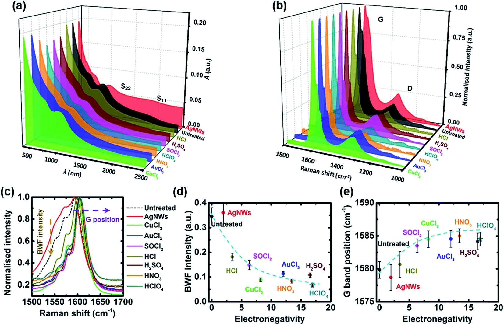 | ||
| Fig. 2 (a) UV-vis-NIR and (b) Raman spectra of untreated, AgNW hybridized, CuCl2, AuCl3, SOCl2, HCl, H2SO4, HNO3 and HClO4 doped GOCNT films; (c) an expanded view of the G band in Raman spectra from 1500 to 1700 cm−1; (d) BWF peak intensity (estimated from Fig. S7†)67,68 of GOCNT films treated with different materials and (e) G band position versus electronegativity. The blue dashed lines (in d and e) do not indicate any prediction but are added to highlight a trend. | ||
The influence of the hybridization and p-type doping on the optoelectronic properties is further studied with measured Rsheet and FOM (calculated by eqn (1) and (2)) versus the sum of electronegativity of the molecules or species acting on the CNTs, as shown in Fig. 3(a and b). Among all of the films, the untreated film has the highest Rsheet with the lowest FOM and the AgNW hybridized GOCNT film has the lowest Rsheet (120 Ω sq−1 (AgNWs–GOCNT hybrids) versus above 350 Ω sq−1 (p-doped GOCNT films)) with the highest FOM (12 (AgNWs–GOCNT hybrids) versus less than 4 (p-doped GOCNT films)), which indicates that the optoelectronic properties of the GOCNT film are significantly improved after the hybridization of AgNWs. Compared to the FOM value (above 90) in the previous literature, our value for AgNW hybridization is much lower, which might be due to the fact that the film in the literature had a much higher content of AgNWs (only 6 wt% SWCNT and the absorption peaks of SWCNTs were not observed in the UV-vis-NIR spectrum for the hybrid at all)69 than the films in this study. In terms of the p-type doped GOCNT films, it seems that the Rsheet/FOM decreases/increases exponentially with the sum of electronegativity of active elements in these dopants. Since the p-type doping is realized by electron transfer from the CNTs to adsorbed dopant molecules, it is not surprising that molecules containing more and/or higher electronegativity atoms have better ability to withdraw electrons. In order to test the validity of this relationship, we decided to use a dopant which had not previously been used in the literature to determine if it followed a similar trend. Doping with HClO4 (electronegativity sum = 16.92) was performed and the Rsheet and FOM seem to fit well in the correlation found before, as shown in Fig. 3(a and b) (the star). In addition, both the bleaching of S11 in the UV-vis-NIR and the upshifting of G band in the Raman spectrum revealed the p-doping nature of HClO4 treatment (Fig. 2).
 | ||
| Fig. 3 (a) Rsheet and (b) FOM as a function of the electronegativity of the active elements in the materials used for hybridization or doping of GOCNT transparent conducting films. The exponential fits (in both a and b) do not include the data points of AgNWs–GOCNT since the hybridization of AgNWs does not shift the Fermi level and charge carrier density and HClO4 treated films. | ||
Overall, hybridization of GOCNTs with AgNWs is the most effective way to enhance the optoelectronic properties of the films, and materials containing active atoms with higher electronegativity values are better dopants than those with lower values. Since the working mechanism of AgNWs (creating a more conductive metallic path between less conductive GOCNT networks, as shown in Fig. S5†) is different from that of p-type dopants, it does not fit the trend found in this study. We used a measure of electronegativity as opposed to (for example) redox potentials because in many cases there is more than one mechanism of action suggested and we used the sum of electronegativity to try to take into account all means of interaction.
3.2 Performance of solar cells
Fig. 4(a and b) show the J–V curves of GOCNT/Si devices with GOCNTs treated with AgNWs and different p-type dopants under AM 1.5 solar simulated light and dark conditions and the detailed performance parameters are shown in Fig. 4(c–l) with the details listed in Tables S1 and S2.† As shown in Fig. 4(c), the efficiency increases with the electronegativity for devices with p-type doped GOCNT films. Interestingly, devices with GOCNT films with the best optoelectronic properties (AgNWs–GOCNT) do not have the highest efficiency. For more details, the values of short circuit current density (JSC) for all devices are very similar (the average values are within the range from 26 to 27 mA cm−2), which is further supported by the fact that the EQE curves all have the same shape and a similar signal intensity, as shown in Fig. 4(d and e). Both the open circuit voltage (VOC) and fill factor (FF) generally increase with the electronegativity (Fig. 4(f and g)). Thus, the trend in efficiency might be due to the combined effect of VOC and FF. The inconsistency in the VOC of AgNWs and AuCl3 treated devices (relatively larger error bars compared to those of other devices) is possibly caused by non-ideal short-circuits caused by the metal nanowires/nanoparticles bridging the front metal electrode (Au/Cr) to the Si layer, which has been observed previously in other reports.21,33 | ||
| Fig. 4 Performance of the solar cells based on GOCNT films with different treatments (a) J–V light curves; (b) J–V dark curves; (c) efficiency; (d) JSC; (e) EQE (the integrated JSC values based on EQE are listed in Table S3†); (f) VOC; (g) FF; (h) Rshunt; (i) Rseries; (j) ideality; (k) Jsat and (l) ϕB. The blue dashed lines in (c), (d) and (f–l) do not indicate any prediction but show the trends in these plots. | ||
The properties of the junction were further studied by analysis of dark J–V curves. The shunt resistance (Rshunt) of the interfaces increases with the electronegativity while the series resistance (Rseries) has a decreasing trend, as shown in Fig. 4(h and i). In terms of the diode properties, there is no clear trend in ideality, Jsat and ϕB due to the relatively large error bars related to the values (Fig. 4(j–l)). However, the general observation is that devices with untreated GOCNT films have poorer diode performance (the highest ideality and Jsat with the lowest ϕB) while solar cells whose films were treated with dopants with a high total electronegativity, such as HNO3 and H2SO4, have excellent diode properties (with ideality approaching 1 and increasing ϕB).
Similarly, when investigating optoelectronic properties, in order to test the validity of the correlation between the efficiency and the sum of the active element electronegativity in the dopants, devices with HClO4 treated top electrodes were fabricated and the results fit well as shown in Fig. 4(c). In addition, most of the other parameters of the HClO4 related devices, including JSC, VOC, FF, Rshunt, Rseries, ideality, Jsat, and ϕB, fit the general trend as other dopants, as shown in Fig. 4. The trend in VOC, FF, ideality and ϕB infers that a better junction has been created between Si and the GOCNT film after different treatments with the improvement in the optoelectronic properties as well as the formation of a better contact.
Overall, the devices treated with dopants with higher electronegativity values for the active elements have better efficiency (HNO3 treated devices have the highest efficiency among them, 11.38 ± 0.26%) as well as the best diode properties while the solar cells fabricated with the films of the best optoelectronic properties (AgNWs–GOCNT) have efficiency just higher than that of control devices (8.14 ± 0.27% versus 7.11 ± 0.35%). This suggests that the performance of the GOCNT/Si heterojunction solar cells is not solely dependent on the optoelectronic properties of the transparent conducting window electrodes. Since AgNWs can significantly enhance the charge transport through the GOCNT network while the improvement in the FOM for p-type doped GOCNT films is mainly due to the increased density of free charge carriers,65 it is inferred that the density of free charge carriers is the most important parameter in improving the solar cell performance. Furthermore, the role of the GOCNT network is more than that of a window electrode to transport the separated holes. More importantly, it contributes to the separation of the excitons by forming a p–n or Schottky junction between Si.
3.3 Stability of the treatment and solar cell performance
Since one of the issues for the industrial application of GOCNT films is the instability of the effects of the treatment, normalized FOM and the efficiency of the solar cells as a function of time were studied, as shown in Fig. 5 and S8.† As shown in Fig. 5(a), the optoelectronic properties of the untreated films are very stable over 10 days while GOCNT films treated with AgNWs, HNO3 and AuCl3 are the most unstable (retaining about 70% of the original value after 10 days). The FOM degradation of the AgNW hybridized GOCNTs is caused by the oxidation of the metal nanowire,70 while the severe desorption of physisorbed NO2 and HNO3 molecules57 and the aggregation of Au nanoparticles71 as well as the desorption of Cl− which may react with air are the potential reasons for the FOM degradation of GOCNT films treated with HNO3 and AuCl3.44 The doping stability of SOCl2 is better than those of the aforementioned three but worse than that of CuCl2. The better stability of CuCl2 treated GOCNT films is due to the Cu2+ hydroxide in the redox dopant, which can persistently withdraw electrons from CNTs over the long term.37 Though HCl seems to be a very stable dopant as well, it has the least effective doping effect on GOCNTs. H2SO4 doped GOCNT films are quite stable for the first few days and then degrade rapidly, which is due to the desorption of HSO4− and H2SO4 molecules and is consistent with previous studies.56 | ||
| Fig. 5 Degradation of (a) FOM, (b) efficiency of solar cells and (c) normalized efficiency divided by FOM (when the value stays at 1 with increasing time, it indicates that the degradation of the solar cell efficiency is solely due to the FOM degradation. Lower values indicate that there is a more serious oxidation effect on the performance degradation). The trend lines in the figures are added to guide the eye. | ||
The degradation of the solar cell performance is shown in Fig. 5(b) and the normalized efficiency divided by FOM is plotted in Fig. 5(c) to study the influence of electrode properties on the solar cell performance. The efficiency decay is mainly caused by a combination of the degradation of the optoelectronic properties of GOCNT films and the growth of the insulating oxide layers (SiOx) between Si and the GOCNT electrode. After 10 days, the untreated devices have an efficiency of about 75% of their original state (this is similar to previous reports),21 which is solely due to the growth of the oxide layer. Solar cells with GOCNT films doped with CuCl2, SOCl2 and HCl (the three most stable dopants) have very similar stability to the control devices while the efficiencies of AgNW, HNO3, AuCl3 and HClO4 (the least stable four dopants) treated devices degrade to about 65% of their starting state. This suggests that the main reason for the degradation might be the growth of SiOx rather than the degradation of the GOCNT optoelectronic properties, which is further evidenced by the fact that the value of the normalized efficiency divided by FOM for most of the treated devices is very similar (about 0.8) and slightly higher than that of the untreated devices (about 0.75) after 10 days (with the exception of H2SO4 treated devices), as shown in Fig. 5(c). Interestingly, H2SO4 doped devices degrade to about 35% efficiency of its starting point within 5 days but the properties of GOCNT films are stable for the first 5 days. In addition, the value of the normalized efficiency divided by FOM for such devices is much lower than that of untreated samples. Both facts suggest that the oxidation rate of Si might be faster for the devices with the H2SO4 treated electrodes due to the presence of oxidizing species (HSO4− and H2SO4).
Different doping strategies have been widely explored and applied to CNT based transparent conducting films in order to improve the optoelectronic properties. As shown in this report, the FOM of GOCNT electrodes is improved using various dopants and the resulting solar cells show improved performance compared to the control devices. The bath doping approach shows excellent compatibility in the processing in terms of dopants, doping periods and the limited adverse effect on the final devices. Based on the results in this report, an ideal dopant would contain atoms of high electronegativity. However, the instability of the doping as well as the devices is still a concern which must be addressed in any commercial development.
4. Conclusion
The optoelectronic properties of GOCNT films were improved with different doping approaches, including incorporation of AgNWs and p-type dopants (CuCl2, AuCl3, SOCl2, HCl, H2SO4, HNO3, and HClO4), and these films were applied in GOCNT/Si heterojunction solar cells to study both the performance and stability of the devices. Among these various agents, using AgNWs is the most effective approach to improve the FOM while dopants with a high total electronegativity of the active atoms, such as HNO3, H2SO4 and HClO4, enhance the efficiency of the solar cells significantly with the best performance recorded for HNO3 doping (11.38 ± 0.26% vs. 7.11 ± 0.35% before doping). CuCl2 and HCl have the best doping stability for the GOCNT films and devices fabricated with such films have the best performance stability.Conflicts of interest
There are no conflicts to declare.Acknowledgements
This work is supported by the South Australian node of both the Australian Microscopy and Microanalysis Research Facility (AMMRF) and the Australian National Fabrication Facility (ANFF). The support of the Australian Research Council Discovery Program (DP150101354 and DP160101301) is gratefully acknowledged. Part of this research was undertaken on the soft X-ray beamline at the Australian Synchrotron, part of ANSTO. Very helpful discussions with Dr Daniel Tune from the Karlsruhe Institute of Technology are gratefully acknowledged.References
- L. Yu, C. Shearer and J. Shapter, Chem. Rev., 2016, 116, 13413–13453 CrossRef CAS PubMed.
- C. Candelise, M. Winskel and R. Gross, Prog. Photovoltaics, 2012, 20, 816–831 Search PubMed.
- B. Zhang, D. M. Liu, Y. T. Liang, D. D. Zhang, H. Yan and Y. Z. Zhang, Mater. Lett., 2017, 201, 50–53 CrossRef CAS.
- M. A. Riza, M. A. Ibrahim, U. C. Ahamefula, M. A. M. Teridi, N. A. Ludin, S. Sepeai and K. Sopian, Sol. Energy, 2016, 137, 371–378 CrossRef CAS.
- Y. Q. Zhang, L. L. Yang and Y. Ge, J. Nanosci. Nanotechnol., 2017, 17, 4931–4935 CrossRef.
- Y. Yu, Y. F. Luo, A. Guo, L. J. Yan, Y. Wu, K. L. Jiang, Q. Q. Li, S. S. Fan and J. P. Wang, Nanoscale, 2017, 9, 6716–6723 RSC.
- S. Pyo, W. Kim, H. I. Jung, J. Choi and J. Kim, Small, 2017, 13, 1700918 CrossRef PubMed.
- Y. Kim, H. R. Lee, T. Saito and Y. Nishi, Appl. Phys. Lett., 2017, 110, 153301 CrossRef.
- Y. He, H. H. Jin, S. Qiu and Q. W. Li, Chem. Commun., 2017, 53, 2934–2937 RSC.
- X. L. Zhang, K. Aitola, C. Hagglund, A. Kaskela, M. B. Johansson, K. Sveinbjornsson, E. I. Kauppinen and E. M. J. Johansson, ChemSusChem, 2017, 10, 434–441 CrossRef CAS PubMed.
- S. K. R. Pillai, J. Wang, Y. L. Wang, M. M. Sk, A. B. Prakoso, Rusli and M. B. Chan-Park, Sci. Rep., 2016, 6, 38453 CrossRef CAS PubMed.
- X. Zhang, W. X. Zhou, X. K. Chen, Y. Y. Liu and K. Q. Chen, Phys. Lett. A, 2016, 380, 1861–1864 CrossRef CAS.
- P. F. Weck, E. Kim and Y. F. Wang, Chem. Phys. Lett., 2016, 652, 22–26 CrossRef CAS.
- Q. Y. Rong, C. Shao and H. Bao, J. Appl. Phys., 2017, 121, 054302 CrossRef.
- Y. D. Liu, F. Q. Wang, Y. J. Liu, X. Z. Wang, Y. B. Xu and R. Zhang, Nanoscale, 2016, 8, 12883–12886 RSC.
- T. Lee, S. Kim, H. Kim, B. S. Kim, Y. S. Lee, J. H. Han and H. J. Paik, Compos. Sci. Technol., 2015, 121, 95–103 CrossRef CAS.
- M. S. Ahmed, H. Jeong, J. M. You and S. Jeon, Electrochim. Acta, 2011, 56, 4924–4929 CrossRef CAS.
- D. V. Vlasov, V. I. Kryshtob, T. V. Vlasova, S. N. Bokova, O. P. Shkarova, E. D. Obraztsova, L. A. Apresyan and V. I. Konov, Polym. Sci., Ser. A, 2012, 54, 34–38 CrossRef CAS.
- S. J. Chen, C. Y. Qiu, A. H. Korayem, M. R. Barati and W. H. Duan, Powder Technol., 2016, 301, 412–420 CrossRef CAS.
- G. Y. Ao, J. K. Streit, J. A. Fagan and M. Zheng, J. Am. Chem. Soc., 2016, 138, 16677–16685 CrossRef CAS PubMed.
- L. Yu, M. Batmunkh, T. Grace, M. Dadkhah, C. Shearer and J. Shapter, J. Mater. Chem. A, 2017, 5, 8624–8634 CAS.
- Y. J. Yang and W. K. Li, Biosens. Bioelectron., 2014, 56, 300–306 CrossRef CAS PubMed.
- C. Y. Yang, J. L. Shen, C. Y. Wang, H. J. Fei, H. Bao and G. C. Wang, J. Mater. Chem. A, 2014, 2, 1458–1464 CAS.
- L. N. Wang, X. L. Jia, Y. F. Li, F. Yang, L. Q. Zhang, L. P. Liu, X. Ren and H. T. Yang, J. Mater. Chem. A, 2014, 2, 14940–14946 CAS.
- G. Z. Sun, X. Zhang, R. Z. Lin, J. Yang, H. Zhang and P. Chen, Angew. Chem., Int. Ed., 2015, 54, 4651–4656 CrossRef CAS PubMed.
- L. Yu, D. Tune, C. Shearer and J. Shapter, ChemSusChem, 2015, 8, 2940–2947 CrossRef CAS PubMed.
- L. Yu, T. Grace, M. D. Jazi, C. Shearer and J. Shapter, Solar RRL, 2017, 1, 1600026 CrossRef.
- L. Yu, D. D. Tune, C. J. Shearer and J. G. Shapter, ChemNanoMat, 2015, 1, 115–121 CrossRef CAS.
- T. Grace, L. Yu, C. Gibson, D. Tune, H. Alturaif, Z. Al Othman and J. Shapter, Nanomaterials, 2016, 6, 52 CrossRef PubMed.
- L. Yu, D. D. Tune, C. J. Shearer and J. G. Shapter, Sol. Energy, 2015, 118, 592–599 CrossRef CAS.
- L. P. Yu, D. Tune, C. Shearer, T. Grace and J. Shapter, IEEE J. Photovoltaics, 2016, 6, 688–695 CrossRef.
- D. D. Tune, B. S. Flavel, R. Krupke and J. G. Shapter, Adv. Energy Mater., 2012, 2, 1043–1055 CrossRef CAS.
- X. Li, Y. Jung, J.-S. Huang, T. Goh and A. D. Taylor, Adv. Energy Mater., 2014, 4, 1400186 CrossRef.
- Y. Jung, X. K. Li, N. K. Rajan, A. D. Tayor and M. A. Reed, Nano Lett., 2013, 13, 95–99 CrossRef CAS PubMed.
- J. M. Harris, M. R. Semler, S. May, J. A. Fagan and E. K. Hobbie, J. Phys. Chem. C, 2015, 119, 23293 CAS.
- J. M. Harris, J. Y. Huh, M. R. Semler, T. Ihle, C. M. Stafford, S. D. Hudson, J. A. Fagan and E. K. Hobbie, Soft Matter, 2013, 9, 11568–11575 RSC.
- K. Cui, Y. Qian, I. Jeon, A. Anisimov, Y. Matsuo, E. I. Kauppinen and S. Maruyama, Adv. Energy Mater., 2017, 7, 1700449 CrossRef.
- Y. Jia, P. Li, X. Gui, J. Wei, K. Wang, H. Zhu, D. Wu, L. Zhang, A. Cao and Y. Xu, Appl. Phys. Lett., 2011, 98, 133115 CrossRef.
- U. N. Maiti, W. J. Lee, J. M. Lee, Y. Oh, J. Y. Kim, J. E. Kim, J. Shim, T. H. Han and S. O. Kim, Adv. Mater., 2014, 26, 40–67 CrossRef CAS PubMed.
- D. J. Yun, Y. J. Jeong, H. Ra, J. M. Kim, J. H. Park, S. Park, T. K. An, M. Seol, C. E. Park, J. Jang and D. S. Chung, J. Phys. Chem. C, 2016, 120, 10919–10926 CAS.
- Y. Li, H. Li, A. Petz and S. Kunsagi-Mate, Carbon, 2015, 93, 515–522 CrossRef CAS.
- S. Ogino, T. Itoh, D. Mabuchi, K. Yokoyama, K. Motomiya, K. Tohji and Y. Sato, J. Phys. Chem. C, 2016, 120, 7133–7143 CAS.
- D. H. Kim, J. K. Lee, J. H. Huh, Y. H. Kim, G. T. Kim, S. Roth and U. Dettlaff-Weglikowska, Phys. Status Solidi B, 2011, 248, 2668–2671 CrossRef CAS.
- S. M. Kim, K. K. Kim, Y. W. Jo, M. H. Park, S. J. Chae, D. L. Duong, C. W. Yang, J. Kong and Y. H. Lee, ACS Nano, 2011, 5, 1236–1242 CrossRef CAS PubMed.
- K. K. Kim, S. M. Kim and Y. H. Lee, Acc. Chem. Res., 2016, 49, 390–399 CrossRef CAS PubMed.
- J. Lee, J. Y. Woo, J. T. Kim, B. Y. Lee and C. S. Han, ACS Appl. Mater. Interfaces, 2014, 6, 10974–10980 CAS.
- D. C. Marcano, D. V. Kosynkin, J. M. Berlin, A. Sinitskii, Z. Sun, A. Slesarev, L. B. Alemany, W. Lu and J. M. Tour, ACS Nano, 2010, 4, 4806–4814 CrossRef CAS PubMed.
- C. Yang, Y. Tang, Z. Su, Z. Zhang and C. Fang, J. Mater. Sci. Technol., 2015, 31, 16–22 Search PubMed.
- J. N. Tey, X. Ho and J. Wei, Nanoscale Res. Lett., 2012, 7, 548 CrossRef PubMed.
- B. Ruzicka, L. Degiorgi, R. Gaal, L. Thien-Nga, R. Bacsa, J. P. Salvetat and L. Forro, Phys. Rev. B: Condens. Matter Mater. Phys., 2000, 61, R2468–R2471 CrossRef CAS.
- S. De and J. N. Coleman, ACS Nano, 2010, 4, 2713–2720 CrossRef CAS PubMed.
- L. Hu, D. S. Hecht and G. Grüner, Nano Lett., 2004, 4, 2513–2517 CrossRef CAS.
- C. J. Shearer, L. Yu, R. Fenati, A. J. Sibley, J. S. Quinton, C. T. Gibson, A. V. Ellis, G. G. Andersson and J. G. Shapter, Chem.–Asian J., 2017, 12, 1625–1634 CrossRef CAS PubMed.
- D. Yang, A. Velamakanni, G. Bozoklu, S. Park, M. Stoller, R. D. Piner, S. Stankovich, I. Jung, D. A. Field, C. A. Ventrice and R. S. Ruoff, Carbon, 2009, 47, 145–152 CrossRef CAS.
- C. Housecroft and A. G. Sharpe, Inorganic Chemistry, Pearson Education Limited, 2007 Search PubMed.
- R. Graupner, J. Abraham, A. Vencelova, T. Seyller, F. Hennrich, M. M. Kappes, A. Hirsch and L. Ley, Phys. Chem. Chem. Phys., 2003, 5, 5472–5476 RSC.
- D. W. Shin, J. H. Lee, Y. H. Kim, S. M. Yu, S. Y. Park and J. B. Yoo, Nanotechnology, 2009, 20, 475703 CrossRef PubMed.
- J. A. Fagan, E. H. Haroz, R. Ihly, H. Gui, J. L. Blackburn, J. R. Simpson, S. Lam, A. R. H. Walker, S. K. Doorn and M. Zheng, ACS Nano, 2015, 9, 5377–5390 CrossRef CAS PubMed.
- M. X. Jing, C. Han, M. Li and X. Q. Shen, Nanoscale Res. Lett., 2014, 9, 588 CrossRef PubMed.
- A. V. Naumov, S. Ghosh, D. A. Tsyboulski, S. M. Bachilo and R. B. Weisman, ACS Nano, 2011, 5, 1639–1648 CrossRef CAS PubMed.
- X. D. Liu, C. X. Chen, L. M. Wei, N. T. Hu, C. J. Song, C. H. Liao, R. He, X. S. Dong, Y. Wang, Q. R. Liu and Y. F. Zhang, Sci. Rep., 2016, 6, 23319 CrossRef CAS PubMed.
- M. S. Dresselhaus, A. Jorio, M. Hofmann, G. Dresselhaus and R. Saito, Nano Lett., 2010, 10, 751–758 CrossRef CAS PubMed.
- M. S. Dresselhaus, G. Dresselhaus, R. Saito and A. Jorio, Phys. Rep., 2005, 409, 47–99 CrossRef.
- S. D. M. Brown, A. Jorio, P. Corio, M. S. Dresselhaus, G. Dresselhaus, R. Saito and K. Kneipp, Phys. Rev. B: Condens. Matter Mater. Phys., 2001, 63, 155414 CrossRef.
- A. M. Rao, P. C. Eklund, S. Bandow, A. Thess and R. E. Smalley, Nature, 1997, 388, 257–259 CrossRef CAS.
- R. Voggu, C. S. Rout, A. D. Franklin, T. S. Fisher and C. N. R. Rao, J. Phys. Chem. C, 2008, 112, 13053–13056 CAS.
- E. H. Hasdeo, A. R. T. Nugraha, M. S. Dresselhaus and R. Saito, Phys. Rev. B: Condens. Matter Mater. Phys., 2014, 90, 245140 CrossRef.
- H.-J. Shin, S. M. Kim, S.-M. Yoon, A. Benayad, K. K. Kim, S. J. Kim, H. K. Park, J.-Y. Choi and Y. H. Lee, J. Am. Chem. Soc., 2008, 130, 2062–2066 CrossRef CAS PubMed.
- T. Tokuno, M. Nogi, J. Jiu and K. Suganuma, Nanoscale Res. Lett., 2012, 7, 1–7 CrossRef PubMed.
- I. K. Moon, J. I. Kim, H. Lee, K. Hur, W. C. Kim and H. Lee, Sci. Rep., 2013, 3, 1112 CrossRef.
- M. Abdullah-Al-Galib, B. Hou, T. Shahriad, S. Zivanovic and A. D. Radadia, Appl. Surf. Sci., 2016, 366, 78–84 CrossRef CAS.
Footnote |
| † Electronic supplementary information (ESI) available. See DOI: 10.1039/c7ta08445e |
| This journal is © The Royal Society of Chemistry 2017 |