
 Open Access Article
 This Open Access Article is licensed under a
 Creative Commons Attribution 3.0 Unported Licence
Transferrable optimization of spray-coated PbI2 films for perovskite solar cell fabrication†
Mikas
Remeika
,
Sonia Ruiz
Raga
,
Shijin
Zhang
and
Yabing
Qi
 *
*
Energy Materials and Surface Sciences Unit (EMSS), Okinawa Institute of Science and Technology Graduate University (OIST), 1919-1 Tancha, Onna-son, Okinawa, Japan. E-mail: Yabing.Qi@OIST.jp
First published on 9th February 2017
Abstract
Ultrasonic spray coating is a promising pathway to scaling-up of perovskite solar cell production that can be implemented on any scale – from table-top to mass production. However, unlike spin-coating, spray coating processes are not easily described by a set of machine-independent parameters. In this work, in situ measurement and modeling of wet film thickness and evaporation rate are presented as a machine-independent description of the ultrasonic spray coating process, and applied to fabrication process optimization for high-performing perovskite solar cells. Optimization based on physical wet film parameters instead of machine settings leads to better understanding of the key factors affecting film quality and enables process transfer to another fabrication environment. Spray coated PbI2 film morphology is analyzed under a range of coating conditions and strong correlation is observed between spray coating parameters and PbI2 film uniformity. Premature precipitation and sparse nucleation are suggested as causes of film non-uniformity, and optimal process parameters are identified. Device fabrication based on the optimized process is demonstrated under ambient conditions with a relative humidity of 50%, achieving a power conversion efficiency of 13% in 1 cm2 area devices, with negligible hysteresis.
1 Introduction
Despite impressive power conversion efficiencies achieved in perovskite-based solar cells,1,2 it remains uncertain how perovskite solar cell fabrication will be scaled to industrial production. Among various methods, ultrasonic spray coating has been proposed as a path to scaling up the production of perovskite based solar cells. Several studies have demonstrated fabrication of one or more layers of perovskite3–8 solar cells by ultrasonic spray coating. Although the previous studies reported optimized recipes, indicating machine settings, these studies did not quantitatively determine wet film characteristics that result in high-performing dry films. If a recipe is to be transferred to a manufacturing environment on a different scale or using equipment of different manufacturers, the properties of the wet film that are necessary to achieve high-performing functional films are more important than specific machine settings, which will vary depending on the machine design. In this work, we demonstrate both an optimized process and a method to determine wet film thickness and evaporation rate, which are key parameters that determine the final film quality.As a new technology reaches a stage where mass production is considered, development focus shifts from champion device performance to reproducibility. Reproducibility between different locations on the substrate must be considered when device size is increased, and reproducibility between different batches must be considered when production volume is scaled up. For devices based on thin film coating, film uniformity is strongly connected to process reproducibility. In this study we develop the strategy to achieve uniform spray-coated films as device area is increased above 1 cm2. We demonstrate that the mm-scale uniformity of spray coated PbI2 films is determined by spray coating conditions. Furthermore, we address the problem of reproducing the result in a different environment and on equipment where current machine settings may not be easily translated. Through a combination of direct measurement and modeling we accurately determine wet film thickness and evaporation rate that correspond to optimal coating quality. By real-time monitoring of laser light interference and scattering by a wet film, we are able to measure in situ the wet film thickness and evaporation rate. Armed with accurate data for a single solvent, we are able to compute an evaporative mass transfer coefficient that is characteristic of the process chamber, and thereon predict evaporation rates for any solvent, based on data available in the literature.
Evaporation of a thin liquid film is a complicated process that is strongly affected by the properties of the evaporating material, air flow pattern in the process chamber, and the geometry of the evaporating film. In this work we demonstrate that with solvent properties available in the literature, air flow pattern can be characterized by in situ measurement of film evaporation rate, and spray pattern geometry can be accounted for by spatially resolved computation using the COMSOL Multiphysics software suite.
By quantitatively characterizing the wet film under various coating conditions we can advance from intuition to quantitative prediction of coated film quality. The method of in situ wet film characterization that we present requires minimal modification to machinery and can be easily adapted to another spray coating system to determine evaporative mass transfer coefficient and wet film thickness as a function of specific machine settings. Once these parameters are known, process recipes become transferrable between the two machines. Even differences in spray patterns due to different sample sizes can be accounted for by local evaporation rate modeling described in this work.
The immediate goal of this work is optimization of the spray coating process to achieve the best uniformity of the PbI2 precursor for the MAPbI3 perovskite film fabrication. In the sequential perovskite formation process,9,10 the final perovskite film thickness is determined by the thickness of the PbI2 layer, as methyl ammonium iodide (MAI) is supplied from solution as much as is necessary to react with PbI2. While the size and quality of perovskite crystal grains is driven by the concentration of the MAI solution16 (see the ESI†), we show that the large scale (mm scale) uniformity of the perovskite films is determined by the uniformity of the PbI2 layer. Therefore, fabrication processes capable of achieving high uniformity of PbI2 film are crucial to scale-up of perovskite solar cell production.
2 Materials and methods
2.1 Materials
Lead iodide (99.99%) was purchased from Tokyo Chemical Industry Co. Ltd. Chlorobenzene, DMF, DMSO, and IPA were purchased from Wako Pure Chemical Industries Ltd. TiO2 nanoparticle paste (90-T) and methylammonium iodide (MAI) were purchased from Dyesol Ltd. 2,2,7,7-Tetrakis(N,N-di-p-methoxyphenylamine)-9,9-spirobifluorene (spiro-MEOTAD) was purchased from Merck Ltd. Acetonitrile (anhydrous), bis(trifluoromethane)sulfonimide lithium salt (Li-TFSI), 4-tert-butyl pyridine (96%), terpineol and titanium diisopropoxide bis(acetylacetonate) were purchased from Sigma-Aldrich. Pre-patterned fluorine-doped tin oxide (FTO) films on 2 mm thick glass substrates were purchased from Opvtech New Energy Co. Ltd. All materials were used as received without further purification. Organic solvents were regular non-dehydrated grade, unless otherwise specified.2.2 Device fabrication
FTO glass substrates were cleaned by brushing with SDS solution, and washing in deionized water followed by ultrasonic cleaning in IPA for 15 min. A compact TiO2 layer was fabricated by spray pyrolysis at 475 °C, using a titanium diisopropoxide bis(acetylacetonate) precursor. The approximate TiO2 compact layer thickness was 40 nm (measured by SEM cross-section imaging). Mesoporous TiO2 was formed by spin coating (4000 rpm, 30 s) TiO2 nanoparticle paste (Dyesol T-90) diluted 1![[thin space (1/6-em)]](https://www.rsc.org/images/entities/char_2009.gif) :3 (by weight) with terpineol, dried (100 °C for 3 min) and annealed (470 °C for 1 hour). Before coating the PbI2, substrate was treated with UV-ozone (15 min). PbI2 was spray coated using a “broad” spray pattern (see below), and heated to 100 °C for 5 min to remove the solvent. PbI2 ink was prepared by dissolving a specified concentration of PbI2 in a mixture of DMF:DMSO, ratio 14:1 by volume. A perovskite layer was formed by immersing the sample in MAI solution (7 mg mL−1 in dehydrated IPA) for 45 s, drying by a nitrogen flow, and annealing at 100 °C for 5 min. A hole transport layer was formed by spin-coating (2000 rpm, 20 s) spiro-MEOTAD solution (72 mg spiro-MEOTAD, 28.8 μL 4-tert-butyl pyridine, 17.5 μL Li-TFSI (520 mg mL−1 in acetonitrile), and 1 mL chlorobenzene). A metallic electrode was formed by thermal evaporation of gold through a shadow mask. All processing (except gold evaporation) was performed in ambient air, with temperature of 23–25 °C and relative humidity 45–55%. Heat was applied using a hot plate in all processing steps. All materials were stored in dry nitrogen and solutions were prepared in a dry nitrogen atmosphere. After preparation, solutions were removed and exposed to air, and stored in sealed containers.
:3 (by weight) with terpineol, dried (100 °C for 3 min) and annealed (470 °C for 1 hour). Before coating the PbI2, substrate was treated with UV-ozone (15 min). PbI2 was spray coated using a “broad” spray pattern (see below), and heated to 100 °C for 5 min to remove the solvent. PbI2 ink was prepared by dissolving a specified concentration of PbI2 in a mixture of DMF:DMSO, ratio 14:1 by volume. A perovskite layer was formed by immersing the sample in MAI solution (7 mg mL−1 in dehydrated IPA) for 45 s, drying by a nitrogen flow, and annealing at 100 °C for 5 min. A hole transport layer was formed by spin-coating (2000 rpm, 20 s) spiro-MEOTAD solution (72 mg spiro-MEOTAD, 28.8 μL 4-tert-butyl pyridine, 17.5 μL Li-TFSI (520 mg mL−1 in acetonitrile), and 1 mL chlorobenzene). A metallic electrode was formed by thermal evaporation of gold through a shadow mask. All processing (except gold evaporation) was performed in ambient air, with temperature of 23–25 °C and relative humidity 45–55%. Heat was applied using a hot plate in all processing steps. All materials were stored in dry nitrogen and solutions were prepared in a dry nitrogen atmosphere. After preparation, solutions were removed and exposed to air, and stored in sealed containers.
2.3 PbI2 film fabrication
Films shown in Fig. 1 were spray coated using a “broad” spray process, see below. PbI2 ink was prepared by dissolving PbI2 in a mixture of DMF:DMSO, ratio 14:1. The mixture of solvents was chosen to make it possible to dissolve a greater concentration of PbI2 than possible for pure DMF at room temperature. Wet film drying rate modeling and measurement was performed for the pure DMF solvent. Accordingly, the evaporation rates specified in Table 1 are for pure DMF. The DMF:DMSO mixture was experimentally measured to have approximately 10% lower evaporation rate than pure DMF, therefore it was considered a good approximation to perform modeling for pure DMF.
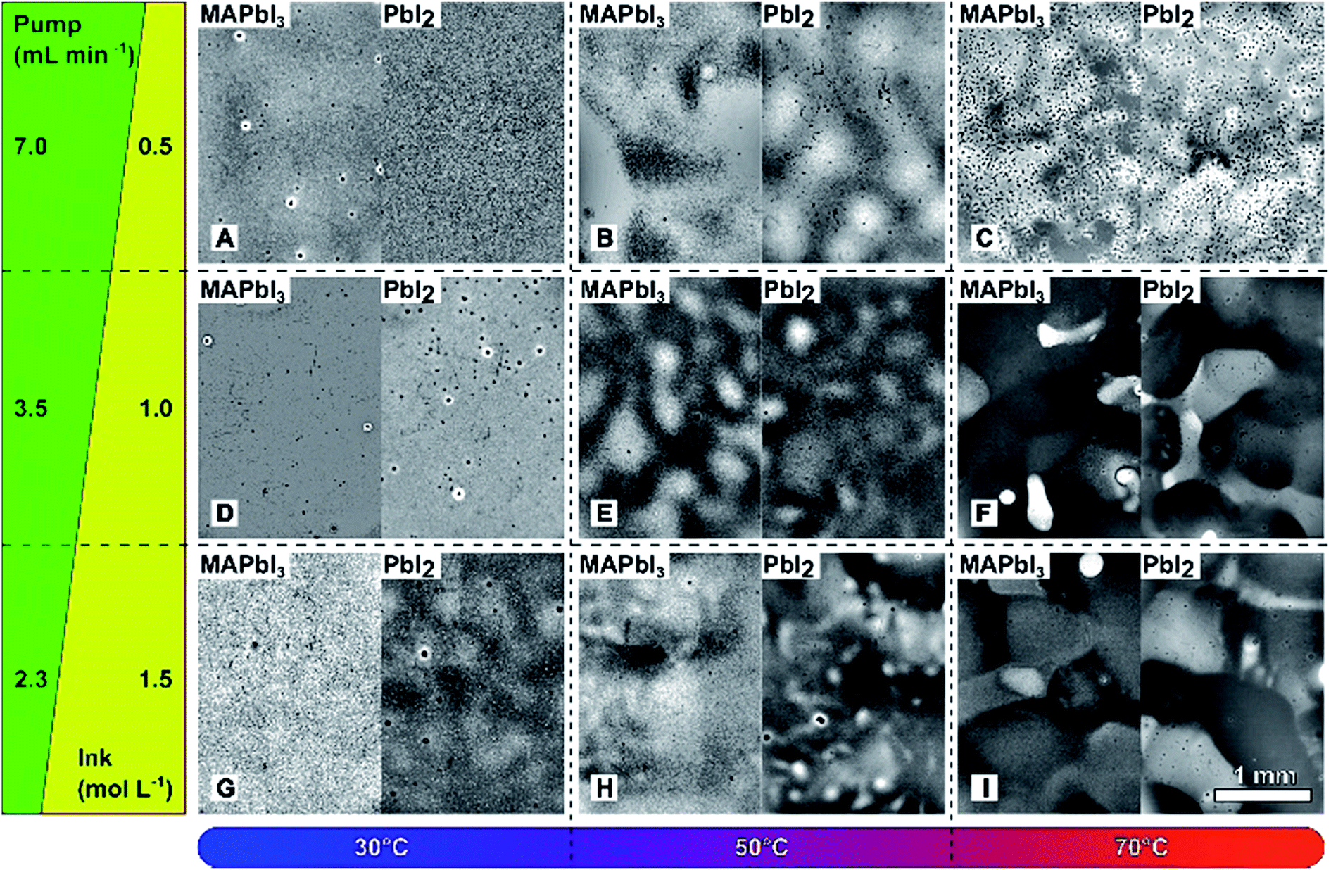 | ||
| Fig. 1 Transmission optical microscope images of (dry) spray-coated PbI2 and corresponding MAPbI3 films at varying substrate temperatures and ink pump rates. Ink pump rate is changed together with the ink concentration, maintaining a constant average PbI2 amount per area. Columns indicate varying process temperatures; rows indicate varying ink pump rates. The PbI2 film was reacted with 7 mg mL−1 MAI in an IPA solution for 45 s to form MAPbI3. The scale bar is 1 mm. | ||
| ID | T/°C | DMF evap. rate/mol m−2 s−1 | Ink pump/mL min−1 | Wet film thick./μm |
|---|---|---|---|---|
| A | 30 | 0.77 | 7.0 | 4.2 |
| B | 50 | 4.2 | 7.0 | 4.2 |
| C | 70 | 13 | 7.0 | 4.2 |
| D | 30 | 0.77 | 3.5 | 2.1 |
| E | 50 | 4.2 | 3.5 | 2.1 |
| F | 70 | 13 | 3.5 | 2.1 |
| G | 30 | 0.77 | 2.3 | 1.4 |
| H | 50 | 4.2 | 2.3 | 1.4 |
| I | 70 | 13 | 2.3 | 1.4 |
2.4 Spray coating parameters
Spray coating was performed using a USI Prism 300 ultrasonic spray coating system, equipped with a CAT-35 ILDS dual mode spray head (operated at 35 kHz, see Fig. S3 in the ESI†). Substrate temperature was controlled by a heated stage. For all coating processes, the substrate was allowed to equilibrate with stage temperature for 3 min before coating. The spray head lateral movement rate was 200 mm s−1, it was operated in “wide” spray mode, and the sample was allowed to dry for 2 min after coating before the process chamber was opened. Coating was accomplished in a single spray pass. For the “broad” spray process, the spray head height above the substrate was 100 mm and the carrier gas (dry N2) pressure was 40 psi, resulting in a wet film pattern approximately 100 mm wide across the direction of head motion. For the “narrow” spray process the head height above the substrate was 30 mm and the carrier gas pressure was 20 psi, resulting in a wet film width of approximately 40 mm.2.5 Sample characterization
X-ray diffraction (XRD) measurements were performed using a Bruker D8 Discover instrument (Bruker AXS K. K., Tokyo, Japan). External quantum efficiency (EQE) measurement was performed on an ORIEL EQE 200 system, operated in DC mode. Integrated Isc was computed from EQE data by assuming an AM1.5G spectrum, without any correction factors. Sample cross-section images were obtained by FIB milling and SEM imaging using a FEI Helios G3 dual beam system. Optical microscope images were obtained using a Leica DM4000 B microscope. Solar cell performance was characterized (in ambient air, with no encapsulation) using an ORIEL Sol1A solar simulator calibrated to 1 sun AM1.5 intensity using a calibrated silicon detector. I–V characteristics were measured using a Keithley 2420 source-measure unit. I–V sweeps were performed from −0.1 V to 1.1 V, steps of 1.2 mV, and dwell time of 100 μs. The sample was illuminated under open circuit conditions for 30 s before measurement.2.6 Evaporation rate computation
Evaporation rates shown in Fig. 3f were determined as follows. For laser reflection measurements, the average liquid evaporation rate was determined from oscillations of reflected beam intensity at room temperature. Using this evaporation rate, the wet film thickness was determined from the linear fit to dry time/pump rate dependence. With known wet film thickness, the average evaporation rate was determined for all temperatures and solvents from the linear fit to the corresponding dry time/pump rate dependence.Evaporation rate by mass change measurement was obtained by multiplying a directly measured rate of wet film weight change by a factor that adjusts for different sample geometries (computed by modeling the local evaporation rate using COMSOL Multiphysics, see Section 3.5).
Model curves combine forced convection and free convection models, as described in the ESI.† Forced convection mass transfer constant was obtained from the direct measurement of mass change in the chamber for a specific solvent. Free convection mass transfer coefficient was calculated as described in ESI,† and multiplied by a geometry correction factor. It is important to note that the value of only one fitting parameter was used to fine tune the model for all solvents and conditions. The geometry correction factor for forced convection was determined completely through modeling of the local evaporation rate using COMSOL Multiphysics, and the ratio between correction factors for narrow and broad spray patterns was also determined from the local evaporation rate model. For IPA, evaporative cooling was taken into account by using reduced liquid surface temperature in the model, for DMF evaporative cooling was deemed negligible (see the ESI†).
2.7 Image processing
Optical images in Fig. 1 were processed to remove intensity variations due to radially varying illumination intensity. Processing was accomplished by subtracting a 3rd order polynomial background automatically computed by GWYDDION 2.44 software.3 Results and discussion
3.1 Challenges in spray coating
Formation of a coated film from solution occurs in two stages: wet film (volatile solvent still present and solids potentially mobile) and dry film (volatile solvents removed and solids no longer mobile). The wet film stage is critical to the formation of a uniform dry film. Prominent causes of non-uniformity that occur in the wet film are film discontinuity, coffee stain effect, and Marangoni flow.Film discontinuity occurs when ink droplets impinging on the substrate do not form a flat wet film, but instead dry as separate droplets. A flat wet film will not form when the ink wetting of the substrate is poor (i.e., with a high liquid contact angle) or when the ink dries faster than the time it takes for the droplets to merge. The chief method of ensuring a good contact angle is to select an ink solvent with surface energy lower than that of the substrate. Wetting can also be improved by adding surfactants to the ink, or by oxygen plasma treatment of the substrate (to increase the surface energy).
The coffee stain effect is a term that is applied to describe accumulation of material at the edges of wet films or droplets. It occurs due to preferential evaporation from a pinned edge of a wet film,11 and can cause an overwhelming fraction of the solids to be deposited at the edges of wet films. The coffee stain effect can be counteracted by inducing Marangoni flow which acts in the opposite direction, for example by addition of a co-solvent with a suitable evaporation rate and surface tension.12 It can also be minimized by creating a wet film with a uniform thickness which will minimize the effective “edge” area. Increasing the substrate temperature will accelerate evaporation, reducing the time available for ink redistribution, however it is not suitable for suppressing the accumulation of ink solids at film edges as it accelerates the coffee stain effect.13
The Marangoni effect is a flow that occurs on the surface of a liquid in the presence of a gradient of surface tension. A flow will occur from the low surface tension region to the high surface tension region. Generally this will occur in cases of a mixture of liquids, and can be used to engineer a flow that counteracts the coffee stain effect,12 however it can also occur in droplets of single solvent and cause accumulation of material in the center of the droplet.14
Another source of non-uniformity that is important to consider is sparse nucleation of precipitate crystals. For salts such as PbI2 deposition will occur preferentially at sites where nucleation has already occurred. Sparse/slow nucleation and a long drying time will result in accumulation of solids in sparse nucleation sites. To achieve the best film uniformity, nucleation rate/density needs to be maximized, and the time during which ink solids are mobile (drying time) needs to be minimized.
3.2 PbI2 spray coating optimization
Measurement of the contact angle of solvents suitable for dissolving PbI2 (DMF, DMSO, and NMP) shows that the liquid contact angle on a TiO2 surface is too low to be measurable (near-perfect wetting). Imaging of individual dried droplets of PbI2 solution (Fig. S1†) shows that visible rings of PbI2 form at the droplet edges and no material accumulates in the droplet center. This indicates that the coffee stain effect is strong for PbI2 dissolved in DMF (or DMSO, NMP), but the Marangoni effect is not observable.To counteract the coffee stain effect by a co-solvent system12 a solvent with a lower surface tension and a lower evaporation rate is required. The surface tensions of DMF, DMSO, and NMP are 34.4 dyn cm−1, 42.9 dyn cm−1, and 40 dyn cm−1, respectively. The boiling temperatures of DMF, DMSO, and NMP are 153 °C, 189 °C, and 202 °C respectively. In this case, low evaporation rate (usually corresponding to a solvent with a high boiling temperature) solvents have a higher surface tension as well, so a co-solvent mixture to counteract the coffee stain effect cannot be prepared from these solvents, and other solvents that dissolve PbI2 are not readily available. Therefore, the remaining pathway to suppressing the coffee stain effect is to minimize the wet film thickness to achieve a faster drying time without increasing the temperature.
Keeping the above guidelines in mind, it is intuitive that the best dry film uniformity would be achieved at a low temperature and a low wet film thickness. Fig. 1 shows transmission light microscope images of spray coated PbI2 and resulting MAPbI3 films fabricated at varying substrate temperatures and wet film thicknesses. The ink concentration is adjusted to maintain the same amount of PbI2 per area in all samples. Table 1 gives the spray coating parameters for each sample in Fig. 1, as well as the calculated wet film thickness and DMF evaporation rate. It is observed that at elevated temperatures (samples B, C, E, F, H and I), thin wet films result in dry films with mm-scale non-uniformity, indicating that precipitation occurred before droplets could form a flat wet film. At the process temperature of 30 °C, films appear uniform in optical images. Detailed examination by AFM (Fig. 2a–c) reveals that perovskite films formed from PbI2 films sprayed at high wet film thicknesses have reduced surface coverage, possibly due to sparse nucleation of PbI2 during film drying and resulting in microscopically uneven films. To quantify this observation, solar cell samples (fabricated as described in Materials and methods) were imaged in AFM after MAPbI3 film formation, before the deposition of the hole transport layer and metal electrode. Fig. 2f shows a clear negative correlation between wet film thickness of the PbI2 spray coating process and surface coverage fraction by MAPbI3.
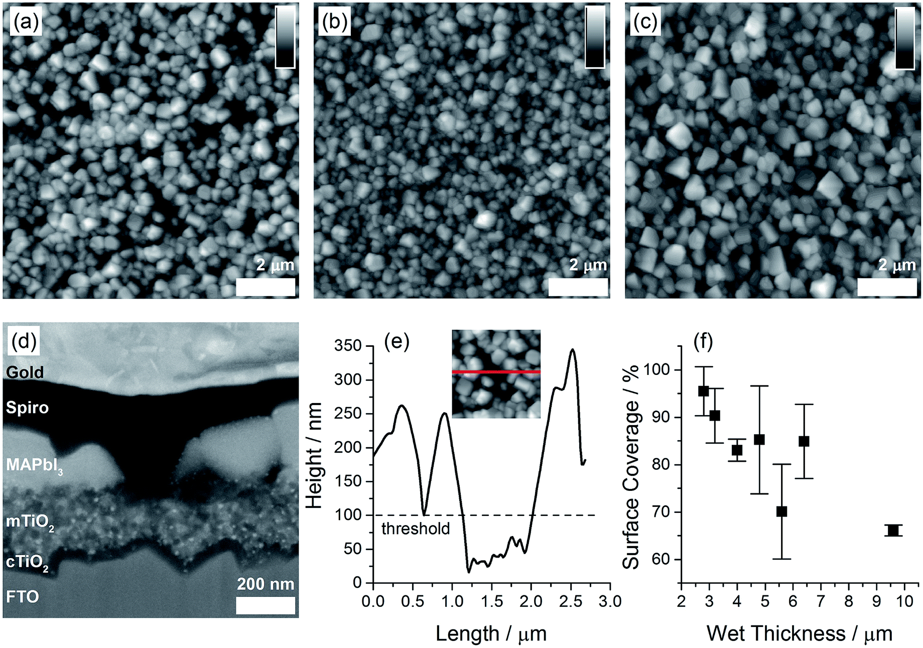 | ||
| Fig. 2 Microscopic morphology dependence on liquid film thickness. (a) AFM topography image of MAPbI3 film formed from sample A (7 mL min−1), (b) sample D (3.5 mL min−1), (c) sample G (2.3 mL min−1). The scale bars are 2.0 μm, grey scale indicates height 0 to 0.5 μm. (d) SEM cross-section image of a device with a void in MAPbI3 film. Scale bar is 200 nm. (f) A sample of a void in MAPbI3 coverage (sample A). The height profile is shown along the red line in the inset. (e) Correlation between surface coverage and wet film thickness of the PbI2 spray coating process. Surface coverage was calculated by excluding the area below a height threshold in AFM images, as illustrated in (e). Wet film thickness was determined as described in Section 3.3. Data collected from 32 samples. Error bars equal to standard deviation. | ||
Data in Fig. 1 demonstrate that the mm-scale uniformity of coated PbI2 films is strongly correlated with spray coating conditions, and that the uniformity pattern of PbI2 films is reflected in the resulting MAPbI3 films. Fig. 2f indicates that a larger wet film thickness results in poorer surface coverage by MAPbI3. A low wet film thickness and a low evaporation rate are optimal for film uniformity. A high evaporation rate results in the mm-scale non-uniformity (i.e., macroscopic non-uniformity), whereas a high wet film thickness results in reduced surface coverage on the μm scale (i.e., microscopic non-uniformity).
3.3 In situ measurement of wet film thicknesses and evaporation rates
As demonstrated above, the optimal coating uniformity is achieved in a narrow range of wet film thickness and evaporation rate. It is then necessary to accurately determine wet film thickness and evaporation rate, so that the optimized recipe can be transferred to other fabrication sites or coating machines. Determining the thickness of the wet film in a spray-coating system is a non-trivial task. While it may appear that with a known spray profile the wet film thickness can be calculated from the amount of liquid ink applied per area, in practice that is not the case. The spray profile is generally unknown and difficult to characterize, the solvent will evaporate from the ink during flight from the spray head to the coating surface, a fraction of the droplets may not reach the substrate, and ink may flow laterally before it achieves a stable thickness. These factors combined make it impractical to approximate the wet film thickness by simple mass conservation, and demand a direct measurement.Fig. 3a shows the principle of operation for a wet film measurement system that allows in situ measurement of wet film thickness in a spray coating system. A laser beam is set up to be reflected from the substrate that is being spray coated. The substrate must be at least partially reflective, a requirement that is readily satisfied by transparent glass-FTO, or glass-ITO substrates typically used for perovskite solar cell fabrication. When a film of pure solvent is sprayed onto the substrate, a fraction of the light is scattered or absorbed, reducing the total amount reaching the detector. Additionally, the wet film creates a second partially reflective surface. The laser beams reflected from the liquid film surface and the substrate surface will interfere constructively or destructively depending on the thickness of the wet film (principle of operation of anti-reflective coatings). If the intensity is tracked in real time, the reflected beam intensity will oscillate. The reflected beam intensity will go through a complete oscillation when the path difference between the beams reflected from the liquid and from the substrate will change by one wavelength. Note that scattering and absorption do not mask the interference as long as they do not change on exactly the same time-scale. If the change of film thickness in one complete oscillation is denoted as Δh then
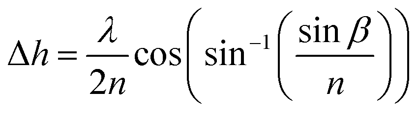 | (1) |
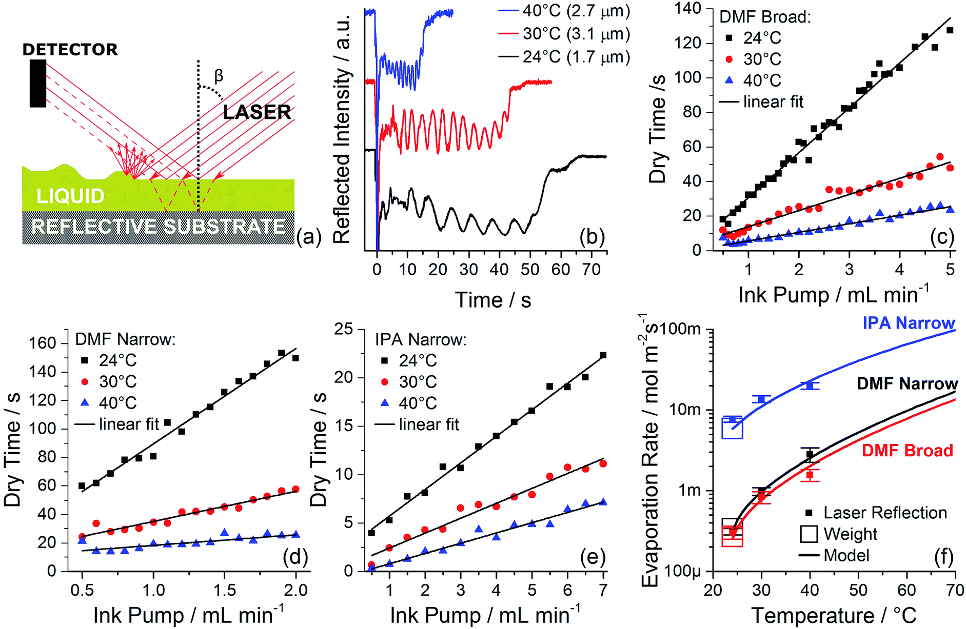 | ||
| Fig. 3 (a) Schematic of the measurement to monitor the wet film thickness change using laser reflection. Laser light reflected by the liquid and substrate surfaces interfere constructively or destructively at the detector depending on the liquid film thickness. A fraction of laser light is scattered or absorbed by the liquid, indicating the presence of the liquid by the reduced total intensity. (b) Oscillations of intensity of the laser light reflected from an evaporating wet film. Temperature and initial wet film thickness for each plot are shown in the legend. Plots offset for clarity. (c) The drying time of a DMF wet film, sprayed with the “broad” spray pattern, vs. ink pump rate, measured by tracking the reduced intensity of a reflected laser beam when a wet film is present. Straight lines are linear fits. (d) Drying time for DMF sprayed with the “narrow” spray pattern. (e) Drying time for IPA sprayed with the “narrow” spray pattern. (f) Evaporation rates determined from dry time and interference measurement (squares with error bars), direct weight change measurement (hollow rectangles), and modeling (lines). Error bars were determined from the fitting error and standard deviation of measurements. | ||
This method assumes that during the majority of the drying time the evaporation rate of the solvent film is constant. This is a good assumption as long as the film thickness does not limit the heat flow available for evaporation. Experimental observation of evenly spaced reflected intensity oscillations supports the assumption that the evaporation rate of a flat wet film is constant once the film is stabilized (see Fig. 3b). Fig. 3c–e show that the drying time depends linearly on the amount of dispensed ink, further supporting the assumption that evaporation rate is independent of film thickness. It is notable that the best accuracy wet film drying time and evaporation rate measurement are obtained when the total drying time is longer than 20 s. This time frame ensures that the measurement time is much longer than the spray coating time (about 0.5 s). Fig. 3c–e show that at temperatures above 40 °C drying time can become less than 10 s. To accurately estimate wet film evaporation rate in this regime modeling is employed as described in Sections 3.4 and 3.5.
To further validate evaporation rates determined from laser reflection and interference, the evaporation rates of DMF and IPA were determined by directly measuring the rates of mass change of a liquid film (with a known area) in the process chamber. Rates measured by laser reflection and direct mass change are shown in Fig. 3f (see Materials and methods for details).
The method based on laser light reflection is effective if the reflectivity of the surfaces is constant and the wet film evaporates completely (no precipitation). This means that ink properties have to be inferred from pure solvent properties. This assumption is valid if the solvent viscosity and evaporation rate are not strongly affected by the presence of the solute. For non-polymer materials such as PbI2 this is a good assumption as even at a saturated concentration, the solvent viscosity is not strongly affected. The evaporation rate will be slightly affected by the presence of the solute in the ink; if necessary, this can be accounted for by Raoult's law.15 It can also be noted that in the presence of the precipitate, after most of the solvent has evaporated, solvent evaporation rate may be substantially reduced if it is absorbed into a porous precipitate and is no longer accurately described by a thin liquid film on a flat surface. Our model addresses only the condition where a continuous liquid surface is present, as in this regime ink solids are highly mobile. We do not address the condition of solvent absorbed in a porous precipitate because in that condition ink solids are no longer mobile over macroscopic (mm-scale) distances.
3.4 Evaporative mass transfer coefficient
To complement and extend the measurement of the evaporation rate by laser reflection from the substrate, we also demonstrate that the evaporation rate of a single solvent (e.g. DMF) at low temperatures can be used to compute the evaporative mass transfer coefficient of the process chamber and predict the evaporation rates of other solvents and temperatures using solvent properties available in the literature.The evaporation rate of a single solvent can be computed as follows:
 | (2) |
The evaporative mass transfer coefficient without external heating is dominated by the air flow due to process chamber exhaust. Computation of the mass transfer coefficient due to a forced air flow requires detailed knowledge of the air flow rate above the evaporating surface, which is very difficult to determine. Instead, the evaporative mass transfer coefficient at room temperature was directly measured by tracking the weight change of the sample placed on a precision scale in the spray coating chamber. Because the evaporation rate is significantly elevated at sample edges, the average evaporation rate depends on the evaporating surface geometry. Therefore, to determine the evaporation rate of a spray-coated wet film, the local evaporation rate was determined by modeling in COMSOL Multiphysics (see details below).
At elevated temperatures buoyant convection dominates the air flow. The mass transfer coefficient for buoyant convection can be computed from the sample geometry, air properties, and heated surface temperature15
 | (3) |
3.5 Modelling of the local evaporation rate
For a finite-sized evaporating surface, there is a significant difference between evaporation near and far from the edges. Therefore, if the evaporative mass transfer coefficient is known for a specific evaporating surface shape, it is necessary to introduce a correction factor to determine the evaporation rate for a different evaporating surface geometry. To compute the correction factor, COMSOL Multiphysics 5.2 software was used to determine the local evaporation rates for an arbitrary-shaped surface. Evaporation was modeled by constraining the concentration of evaporating species to match the saturation pressure across the evaporating surface and computing the flux of evaporating species, with appropriate temperature and air flow distributions. Air flow distribution in a realistic geometry is very difficult to compute, therefore it is approximated by a laminar flow set to achieve an experimentally measured average evaporation rate. The experimental value of the average evaporation rate was determined by tracking the change of weight of a square substrate completely covered with DMF, placed on a precision scale in the spray process chamber. Fig. 4 shows an example computation of a difference between evaporation rates at the sample edges and center. The average evaporation rate for a 15 × 15 mm area at the center of a 50 × 50 mm surface of evaporating liquid surface is 0.77 of the rate averaged over the entire liquid surface (including the edges). | ||
| Fig. 4 COMSOL simulation of evaporation rate from a 50 mm wide surface under a laminar air flow in the positive x direction. The evaporating surface extends from x = 2.5 cm to 7.5 cm. (a) Evaporation rate as a function of position. The average evaporation rate over the entire evaporating surface is 4.0 mmol m−2 s−1, and 3.1 mmol m−2 s−1 over the sample area. (b) Concentration of vapor above the sample, normalized by saturation concentration. Arrows indicate direction of air flow. Arrow length is proportional to the computed air flow velocity for laminar flow near the surface. Computation was performed with parameters corresponding to DMF, with surface temperature equal to ambient temperature (24 °C). | ||
Local evaporation rate modeling can also be used to compute the evaporation rate adjustment when spray patterns are changed, as would be expected to happen when scaling-up to higher volume production. Fig. 3f shows evaporation rates computed for a broad DMF spray pattern (100 mm) and a narrow spray pattern (40 mm).
To summarize, results of three complementary approaches to determining the evaporation rate of a film are shown in Fig. 3f. The film evaporation rate and film thickness can be completely determined immediately following spray coating by interference and scattering of a reflected laser beam. Once the laser reflection measurement is accomplished for a single solvent and several temperatures, the evaporative mass transfer coefficient of the process chamber can be computed and applied to predict evaporation rates of different solvents and at temperatures where the film evaporation rate is too fast for accurate measurement. The laser reflection measurement and modeling are verified by a direct measurement of mass change of a wet film of a known area. The set of process parameters to achieve optimal PbI2 film uniformity are: temperature = 30 °C and ink pump rate = 3.5 mL min−1, corresponding to wet film thickness 2.1 μm and DMF evaporation rate of 0.77 mmol s−1 m−2.
3.6 Device fabrication
In this study we focus on the optimization of process parameters to achieve optimal uniformity of spray-coated PbI2 films and characterization of the process in terms of machine-independent parameters. As the ultimate application of this work is the fabrication of perovskite solar cells, it is necessary to demonstrate that the analyzed films indeed result in high performance solar cells.To demonstrate complete devices incorporating a spray coated PbI2 layer, we chose a commonly used perovskite solar cell architecture that is known to be compatible with ambient processing.10Fig. 5a shows the layer structure of the cell and a scanning electron microscopy (SEM) cross-section image of the optimized design. The spray coating process for PbI2 films was selected to match the film with the best uniformity (sample D, temperature = 30 °C and ink pump rate = 3.5 mL min−1). Device performance data for non-optimal wet film thickness can be found in ESI Fig. S8.† As expected, the perovskite solar cells fabricated using the optimal parameters show not only the highest PCE, Voc, Jsc, and FF, but also the lowest standard deviations, strongly suggesting the significantly improved device reproducibility under the optimal coating conditions.
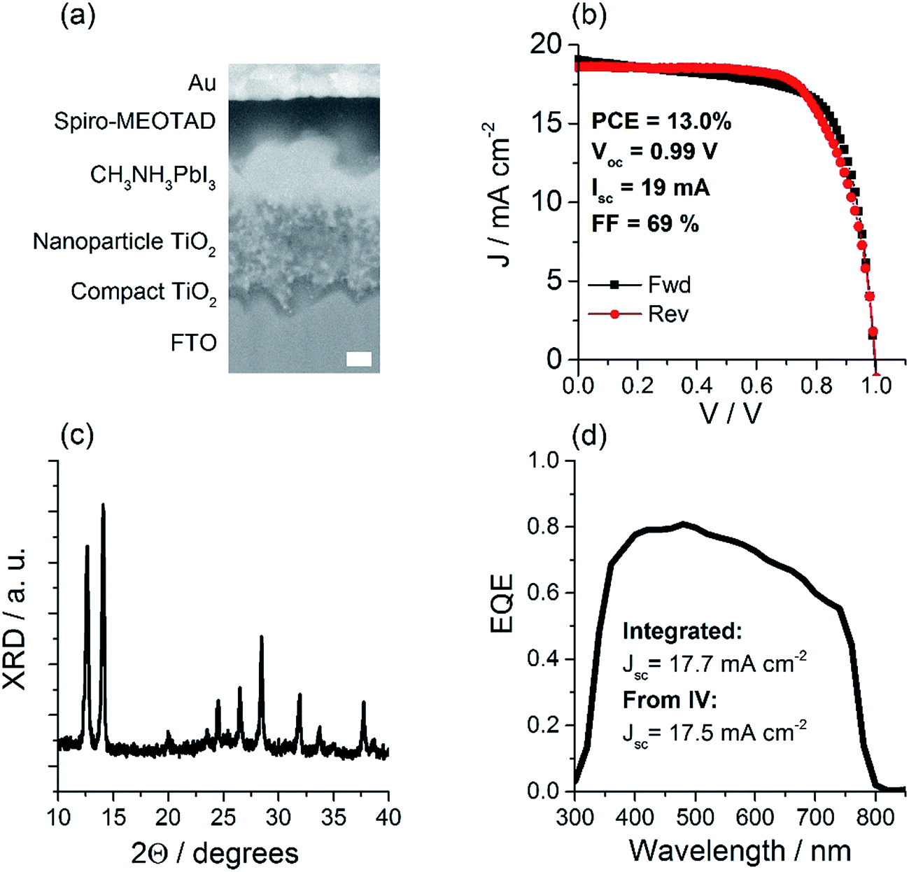 | ||
| Fig. 5 (a) Device layer structure and SEM cross-section image for a solar cell fabricated with spray-coated PbI2. The cross-section was produced by FIB milling. Scale bar is 100 nm. (b) I–V characteristic of a top-performing device. Red (black) curve denotes reverse (forward) sweep. Good agreement between forward and reverse sweeps indicates negligible hysteresis. Device area is 1.1 cm2, masked to 1.0 cm2 for measurement. (c) XRD diffractogram of a typical MAPbI3 film formed from a spray-coated PbI2 film. (d) EQE spectrum of a typical solar cell fabricated with a spray-coated PbI2 film. | ||
Fig. 5c shows the XRD diffractogram of a typical device. Peaks at 2Θ = 14.1° corresponding to MAPbI3 and 2Θ = 12.7° corresponding to unreacted PbI2 are observed. The external quantum efficiency (EQE) spectrum shown in Fig. 5d shows slightly greater EQE at shorter wavelengths, also suggesting the presence of unreacted PbI2. In several recently published studies it has been suggested that residual PbI2 may be difficult to eliminate in a 2-step process, and may not necessarily lead to substantial performance loss. Ko et al.10 implemented a 2-step perovskite formation process under ambient conditions and found that optimal performance was obtained with PbI2 peak in the XRD pattern around 50% as high as MAPbI3 peak. Kim et al.17 discussed in detail the formation process of the MAPbI3 in a 2-step process, and concluded that excess PbI2 cannot be eliminated by simple optimization of MAI solution concentration and immersion time, without compromising the performance. On the other hand, it is expected that further enhancement of MAPbI3 crystallinity can lead to increased performance.
Table 2 shows performance statistics for devices incorporating a spray-coated PbI2 layer. Maximum power conversion efficiency (PCE) of 13.0% is achieved with the average PCE of 10.2%. Device performance is on par with the best performance achieved for spray coated devices with an active area of 1 cm2.8 We also observed that these devices could be operated at the maximum power point for over a 100 hours preserving 60% of initial PCE. See Fig. S7 in the ESI† for steady state measurement of device performance. Thus, we can confirm that the PbI2 films for which uniformity was optimized are suitable for high-performance perovskite solar cell fabrication.
| Parameter | Average | St. dev. | Best |
|---|---|---|---|
| PCE (%) | 10.2 | 1.70 | 13.0 |
| V oc (V) | 0.96 | 0.034 | 1.02 |
| J sc (mA cm−2) | 16.8 | 1.43 | 18.8 |
| FF (%) | 63.1 | 5.41 | 71.9 |
| Hysteresis | 0.13 | 0.10 | 0.006 |
4 Conclusions
We have demonstrated an optimized set of parameters for achieving the best uniformity of ultrasonic spray-coated PbI2 films, at a thickness suitable for high performance perovskite solar cell fabrication. We observe a strong correlation between wet film thickness, evaporation rate and uniformity of dry films, and identify wet film thickness and evaporation rate as key parameters to dry film quality. To enable expedient transfer of a recipe from the specific equipment in the laboratory to the manufacturing environment, we demonstrate a simple way to in situ measure wet film thickness and evaporation rate. Furthermore, we demonstrate that evaporation rate measurement of a single wet film can be used to determine the evaporative mass transfer coefficient of the process chamber. Knowledge of evaporative mass transfer coefficient allows us to compute evaporation rates for inks based on any solvent. We also demonstrate modelling of the local evaporation rate which makes it possible to compute necessary adjustment to process parameters when changing the sample geometry. Using optimal process conditions, we fabricated perovskite solar cells, device performance of which is on par with the best performance achieved for spray coated devices with an active area of 1 cm2.Acknowledgements
This work was supported by funding from the Energy Materials and Surface Sciences Unit of the Okinawa Institute of Science and Technology Graduate University and the OIST R&D Cluster Research Program. We would like to thank M. R. Leyden for assistance with module fabrication.Notes and references
- D. Bi, C. Yi, J. Luo, J. D. Décoppet, F. Zhang, S. M. Zakeeruddin, X. Li, A. Hagfeldt and M. Grätzel, Nat. Energy, 2016, 1, 16142 CrossRef CAS.
- J. W. Lee and N. G. Park, MRS Bull., 2015, 40, 654 CrossRef CAS.
- A. T. Barrows, A. J. Pearson, C. K. Kwak, A. D. F. Dunbar, A. R. Buckley and D. G. Lidzey, Energy Environ. Sci., 2014, 7, 2944 CAS.
- Z. Liang, S. Zhang, X. Xu, N. Wang, J. Wang, X. Wang, Z. Bi, G. Xu, N. Yuan and J. Ding, RSC Adv., 2015, 5, 60562 RSC.
- S. Das, B. Yang, G. Gu, P. C. Joshi, I. N. Ivanov, C. M. Rouleau, T. Aytug, D. B. Geohegan and K. Xiao, ACS Photonics, 2015, 2, 680 CrossRef CAS.
- J. G. Tait, S. Manghooli, W. Qiu, L. Rakocevic, L. Kootstra, M. Jaysankar, C. A. Masse de la Huerta, U. W. Paetzold, R. Gehlhaar, D. Cheyns, P. Heremans and J. Poortmans, J. Mater. Chem. A, 2016, 4, 3792 CAS.
- D. K. Mohamad, J. Griffin, C. Bracher, A. T. Barrows and D. G. Lidzey, Adv. Energy Mater., 2016, 1600994, DOI:10.1002/aenm.201600994.
- H. Huang, J. Shi, L. Zhu, D. Li, Y. Luo and Q. Meng, Nano Energy, 2016, 7, 352 CrossRef.
- J. Burschka, N. Pellet, S.-J. Moon, R. Humphry-Baker, P. Gao, M. K. Nazeeruddin and M. Grätzel, Nature, 2013, 499, 316 CrossRef CAS PubMed.
- H.-S. Ko, J.-W. Lee and N.-G. Park, J. Mater. Chem. A., 2015, 3, 8808 CAS.
- R. D. Deegan, O. Bakajin, T. F. Dupont, G. Huber, S. R. Nagel and T. A. Witten, Nature, 1997, 389, 825 CrossRef.
- Y. Oh, J. Kim, Y. J. Yoon, H. Kim, H. G. Yoon, S.-N. Lee and J. Kim, Curr. Appl. Phys., 2011, 11, S359 CrossRef.
- D. Soltman and V. Subramanian, Langmuir, 2008, 24, 2224 CrossRef CAS PubMed.
- H. Hu and R. G. Larson, J. Phys. Chem. B, 2006, 110, 7090 CrossRef CAS PubMed.
- T. L. Bergman, A. S. Lavine, F. P. Incropera and D. P. Dewitt, Fundamentals of Heat and Mass Transfer, Wiley, Hoboken, NJ, USA, 2011 Search PubMed.
- J.-H. Im, I.-H. Jang, N. Pellet, M. Grätzel and N.-G. Park, Nat. Nanotechnol., 2014, 9, 927 CrossRef CAS PubMed.
- S. Y. Kim, H. J. Jo, S. J. Sung and D. H. Kim, APL Mater., 2016, 4, 100901 CrossRef.
Footnote |
| † Electronic supplementary information (ESI) available. See DOI: 10.1039/c6ta09922j |
| This journal is © The Royal Society of Chemistry 2017 |